This is a repository copy of
Interwell relaxation times in p-Si/SiGe asymmetric quantum
well structures: the role of interface roughness
.
White Rose Research Online URL for this paper:
http://eprints.whiterose.ac.uk/4325/
Article:
Califano, M., Vinh, N.Q., Phillips, P.J. et al. (10 more authors) (2007) Interwell relaxation
times in p-Si/SiGe asymmetric quantum well structures: the role of interface roughness.
Physical Review B, 75 (4). Art. No. 045338. ISSN 1550-235x
https://doi.org/10.1103/PhysRevB.75.045338
[email protected] http s ://eprints.whiterose.ac.uk/ Reuse
See Attached
Takedown
If you consider content in White Rose Research Online to be in breach of UK law, please notify us by
promoting access to White Rose research papers
White Rose Research Online
Universities of Leeds, Sheffield and York
http://eprints.whiterose.ac.uk/
This is an author produced version of a paper published in
Physical Review B.
White Rose Research Online URL for this paper:
http://eprints.whiterose.ac.uk/4325/
Published paper
Califano, M., Vinh, N.Q., Phillips, P.J., Ikoni
ć
, Z., Kelsall, R.W., Harrison, P.,
Pidgeon, C.R., Murdin, B.N., Paul, D.J., Townsend, P., Zhang, J., Ross, I.M.
and Cullis, A.G. (2007)
Interwell relaxation times in p-Si/SiGe asymmetric
quantum well structures: the role of interface roughness,
Physical Review B,
Volume 75 (4), 045338-1 -045338-6.
Interwell relaxation times in p-Si/SiGe asymmetric quantum well structures: the role
of interface roughness
Marco Califano1
, N. Q. Vinh2
, P. J. Phillips3
, Z. Ikoni´c1
, R. W. Kelsall1
, P. Harrison1
C. R. Pidgeon3
, B. N. Murdin4
, D. J. Paul5
, P. Townsend5
, J. Zhang6
, I. M. Ross7
and A. G. Cullis7
1
Institute of Microwaves and Photonics, School of Electronic and Electrical Engineering, University of Leeds, Leeds LS2 9JT, United Kingdom
2
FOM Institute for Plasma Physics “Rijnhuizen”, P.O. Box 1207, NL-3430 BE Nieuwegein, The Netherlands
3
Department of Physics, Heriot-Watt University, Edinburgh, EH14 4AS, United Kingdom
4
Advanced Technology Institute, University of Surrey, Guildford, GU2 7XH, United Kingdom
5
Cavendish Laboratory, University of Cambridge, Cambridge, CB3 0HE, United Kingdom
6
Department of Physics, Imperial College, London, SW7 2BZ, United Kingdom and
7
Department of Electronic and Electrical Engineering, University of Sheffield, Sheffield, S1 3JD, United Kingdom
(Dated: June 5, 2008)
We report the direct determination of non-radiative lifetimes in Si/SiGe asymmetric quantum well structures designed to access spatially indirect (diagonal) interwell transitions between heavy-hole ground states, at photon energies below the optical phonon energy. We show both experimentally
and theoretically, using a six-bandk·pmodel and a time-domain rate equation scheme, that, for the
interface quality currently achievable experimentally (with an average step height≥1 ˚A), interface
roughness will dominate all other scattering processes up to about 200 K. By comparing our results
obtained for two different structures we deduce that in this regimebothbarrierandwell widths play
an important role in the determination of the carrier lifetime. Comparison with recently published experimental and theoretical data obtained for mid-infrared GaAs/AlGaAs multiple quantum well systems leads us to the conclusion that the dominant role of interface roughness scattering at low temperature is a general feature of a wide range of semiconductor heterostructures not limited to IV-IV materials.
PACS numbers:
I. INTRODUCTION
Following the success of III-V quantum cascade lasers (QCLs) both at mid-infrared [1] and far-infrared (ter-ahertz) frequencies [2, 3], there is considerable inter-est in the development of silicon-based quantum cas-cade devices for low cost sources and optoelectronic in-tegration with other circuitry. The indirect bandgap that has hindered interband emitter development in Si, Si1−xGex and Ge does not affect QCLs, as they rely on
carrier transitions within the same (conduction or va-lence) band rather than on exciton recombination across the bandgap. Indeed SiGe-based materials have a ma-jor advantage over III-Vs for this type of device, in that phonons are non-polar [4], and this reduces the principal non-radiative scattering rate that limits the efficiency in III-V devices [2]. This is particularly true at photon ener-gies below the optical phonon energy (~ω <~ωopt) which
range is the subject of the present work.
If a QCL could be realised in Si/SiGe, the lack of po-lar optical phonon scattering, the lower free carrier ab-sorption and the higher thermal conductivity of Si could allow significantly higher operating temperatures in the THz range. Moreover there could be lower manufacturing costs involved with the mature silicon process technology. We have previously demonstrated the first electrolumi-nescence from p-Si/SiGe quantum cascade emitters at THz frequencies [5], however no significant optical gain or
stimulated emission have been achieved so far in Si/SiGe QC structures. In order to achieve a silicon-based QCL, a structure that can achieve population inversion and high gain has to be designed. Of paramount importance to this end is the ability to engineer carrier lifetimes.
The intersubband lifetimes of both inter- and intra-well transitions can be tailored by carefully designing the thickness and the composition of the different lay-ers that form the QC structure. A tunability with bar-rier width has been demonstrated previously at energies above~ωopt, where lifetimes varying between 20 ps and
2
theoretical [9] and experimental [11] studies have found that IFR scattering is a major limiting factor for the low-temperature mobility of 2D hole gases in quantum wells (QWs) narrower than about 5 nm.
Here we present the results of a theoretical and exper-imental investigation into the effects of IFR scattering on the lifetime of diagonal (i.e., interwell) intersubband transitions between heavy-hole (HH) ground states in two different p-SiGe coupled asymmetric quantum wells (CAQWs) in this size range. The experimental informa-tion is provided uniquely by time resolved measurements with a far-infrared pulsed free-electron laser. Such a de-vice is the only laser source that has a short enough pulse duration and high enough intensity to pump and probe the fast recovery transition in this wavelength range. It also provides wide wavelength coverage for HH-HH and HH-LH transitions, and continuous tunability for reso-nant excitation [4]. In contrast, the previously reported data on decay times in p-Si/SiGe QC structures [6] were obtained indirectly from electroluminescence measure-ments. The extraction of subband lifetimes in that case was therefore based on a number of assumptions which may have limited the accuracy of the deducted values. Here, by using a pump-probe technique, we measure di-rectlythe decay time from the upper HH1 ground state to the lower HH1 ground state in the adjacent quantum well. Furthermore, unlike in Ref. [6], in the present case the structures are specifically designed so that between these two levels there is no other state that could provide alternative relaxation pathways, allowing an unambigu-ous determination of the upper state lifetime. We show that we can achieve very long lifetimes (∼70 ps), which exhibit a relative insensitivity to the temperature com-pared to GaAs devices [2].
We calculate IFR scattering rates, compare them with the rates of other mechanisms, such as scattering due to alloy disorder, acoustic and optical phonons as well as carrier-carrier interaction (all calculated within a time-domain rate equation scheme [4]) and predict that, de-spite the good quality of our interfaces (with an average roughness step height of only 1.2-1.5 ˚A), IFR will con-stitute more than 50% of the total scattering rate up to ∼100 K, remaining stronger than any of the other scattering processes up to about 200 K. We show that in this regime both barrier and well widths need to be carefully designed in order to achieve the desired inter-subband transition rates. Our theoretical results are in very good agreement with our measured lifetimes in the temperature range experimentally investigated.
II. EXPERIMENTAL DETAILS
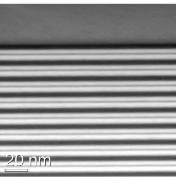
[image:4.595.353.526.50.226.2]We have investigated two strain-symmetrized Si/SiGe CAQW structures on (001) Si, utilising pump/probe spectroscopy of HH interwell transitions to measure the non-radiative recombination by diagonal (bound to bound) HH1-HH1 transitions through the Si barrier. The
FIG. 1: An annular dark field scanning transmission electron micrograph showing the first 8 sets of pairs of QWs and the barriers for the first structure (BF1499).
structures considered in the present study (BF1499 and BF1500) consist of 20 periods each containing CAQWs grown on a relaxed buffer of Si0.8Ge0.2. The first
(BF1499) has 3.4 nm and 4.6 nm undoped SiGe wells with a nominal Ge content of 40%, separated by a Si barrier of 1.8 nm. The second wafer (BF1500) has 3.2 nm and 4.15 nm undoped SiGe wells with a nominal Ge content of 40%, separated by a 2.3 nm Si barrier. The pairs of CAQWs are separated by a 5 nm Si barrier, the central 3.2 nm of which is modulation doped with B to a concentration of NA = 1.6×1018 cm−3. The layer
thicknesses have been measured by transmission electron microscopy (TEM) using high angle angular dark field (HAADF) imaging (see Fig. 1), while the as-grown Ge contents (slightly lower than the nominal ones) were ob-tained using z-contrast HAADF, calibrated with energy dispersive x-ray analysis of the thick SiGe buffer layer.
3
50 100 150
z (Å) -0.2 -0.1 0 0.1 0.2
Energy (eV) 2
1
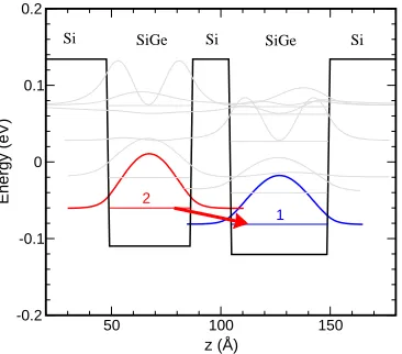
[image:5.595.344.539.48.316.2]Si SiGe Si SiGe Si
FIG. 2: (Color online) Calculated subband structure of
BF1499 showing the energy levels and the square of the wave-functions of the first 8 hole states (we use an electron-like pic-ture where the energy scale is reversed: the ground state is the lowermost). The slightly different depths of the two wells shown reproduces the slight difference in Ge content between them found in our HAADF measurements in all periods im-aged. The interwell non-radiative transition between level 2 (red) and level 1 (blue) is indicated by a red arrow.
micropulses of duration ∼10 ps and 25 MHz repetition rate. A pump-probe technique (or transient bleaching technique) in which the FELIX beam is split into pump, probe and reference beams was used [15]. The samples were mounted in vacuum on the cold finger of a liquid he-lium continuous flow cryostat, with temperature variable from 4.2 K to 300 K. In order to access the HH-HH tran-sitions it was necessary to pump and probe at oblique incidence, enabling the polarization selection ruleE par-allel to the growth direction. The experiments have been performed with the wavelength of FELIX tuned to the absorption peak of the subband transition at 61.3 µm. Figure 3 shows the transient bleaching signal for sample BF1499 as a function of time delay between probe and pump measured for different values of the FELIX pump power at 10 K (a), and for different temperatures (b).
III. THEORETICAL MODEL
IFR is characterised by the average height ∆ and lat-eral size (correlation length) Λ of the Gaussian fluctua-tion of the local posifluctua-tion of the interface with respect to an ideally flat surface, described by the autocorrelation function
S(r) =h∆(r)∆(r′)i= ∆2
exp
−|r−r′| 2
Λ2
(1)
A change ∆(r) in the well width Lat the position r =
(x, y) in the plane, causes a fluctuation
δE0(r) =
∂E0
∂L∆(r)
-20 0 20 40 60 80 100 120 0.1 1 4 K 50 K 100 K 120 K T ra n sm is si o n c h a n g e ( a rb . u n its )
Delay time (ps)
-20 0 20 40 60 80 100 120 0.1 1 T ra n sm is si o n c h a n g e ( a rb . u n its )
Delay time (ps)
0 dB 5 dB 10 dB 13 dB 15 dB 18 dB 25 dB 28 dB 30 dB (b)
Differential Transmission Change (arb.units)
(a)
FIG. 3: (Color online) Power (a) and temperature (b)
depen-dence of the interwell transition lifetimes, measured atT = 4
K for BF1499. In (a) the power decreases with attenuation from 0 to 30 dB.
in the carrier quantisation energyE0. The related
scat-tering matrix element [10]
|hmk′|δE0|nki|2
= Z d2
rFmn∆(r)eiq·r
2 (2)
(whereFmn contains the product of the wave functions
and the potential jumpδE0 at the interface), is
propor-tional to the Fourier transform of the autocorrelation function (1)
S(q) =π∆2
Λ2 exp −q 2 Λ2 4 . (3)
If the Fermi wave vector is much smaller than Λ−1
(the effective cut-off wave vector for the momentum exchange
q), then S(q) ≈ π(∆Λ)2
. In this limit the matrix ele-ments depend only on the product ∆Λ. This is however not the case with our samples and, for a given value of the product ∆Λ =p0˚A
2
, we have found large differences between the lifetimes calculated with [∆ = 1 ˚A , Λ =p0
˚
A] and [∆ = 4 ˚A , Λ = p0/4 ˚A], which increased with
decreasing carrier temperature.
[image:5.595.87.270.51.212.2]4
0 50 100 150
Tlatt (K)
0 50 100 150 τ (ps)
0 50 100
Tlatt (K)
0 100 200 300 τ (ps)
∆ = 1.2 Å Λ = 60 Å
BF1500
BF1499
δT = 20 K
BF1500 barrier BF1499 wells with
perfect interfaces (no IFR scattering)
FIG. 4: (Color online) Comparison of experimentally mea-sured (symbols) and theoretically predicted (lines) interwell
transition lifetimes as a function of lattice temperatureTlatt
for our two samples BF1499 (red) and BF1500 (blue). The red symbols are extracted from single exponential fits to the data in Fig. 3b. The dashed line represents the calculated lifetime for a hypothetical structure with the wells of BF1499 and the barrier of BF1500. Inset: lifetimes calculated for BF1500 and BF1499 in the case of perfect interfaces, i.e., in the absence of IFR scattering (the experimental data are the same as in
the mainframe). All curves were obtained using ∆ = 1.2 ˚A ,
Λ = 60 ˚A , andTh=Tlatt+ 20 K.
the case of electrons [10], however in the present work the quantity Fmn had to be modified to allow each of
the wave function components to experience a different potential at the interface, according to its (heavy-hole, light-hole or split-off) character. The transition rates due to optical and acoustic phonon, alloy disorder, and hole-hole scattering were calculated as described previously [14, 16]. The total scattering rates due to all the decay mechanisms were then employed in a multi-subband rate equation model [14, 16] to track the time evolution of hole population over subbands, following the initial exci-tation.
IV. RESULTS AND DISCUSSION
Due to the lack of detailed experimental information on the quality of our samples interfaces, we resorted to the standard [8, 12, 17] procedure of treating ∆ and Λ as fitting parameters. We deduced their values from the temperature dependence of the decay time in one struc-ture (BF1499) and then used them in the calculation of the lifetimes of the other structure (BF1500), obtaining very good agreement with our measured data, as shown in Fig. 4. Our best fits are obtained with ∆ = 1.2-1.5 ˚
A and Λ = 40-60 ˚A suggesting good quality interfaces. These IFR parameters are also within the range of val-ues reported in the literature [9, 11, 12, 18] (∆ = 1-4 ˚A , Λ = 23-300 ˚A , ∆Λ = 60-1200 ˚A2
) for Si/SiGe interfaces with various Ge content. Interestingly, the value ∆ = 1.5
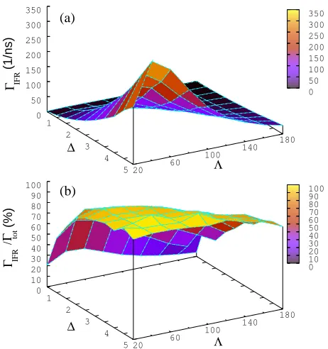
IFR tot IFR 0 50 100 150 200 250 300 350 1 2 3 4 5 20 60 100 140 180 0 50 100 150 200 250 300 350 0 10 20 30 40 50 60 70 80 90 100 1 2 3 4 5 20 60 100 140 180 0 10 20 30 40 50 60 70 80 90 100 (a) (b) Γ /Γ (%) Γ (1/ns) ∆ ∆ Λ Λ
FIG. 5: (Color online) Absolute (a) and relative (b) IFR scat-tering rates as a function of the IFR parameters ∆ and Λ
calculated for BF1499 at Tlatt = 20 K, assuming a carrier
temperature of 40 K.
˚
A was also assumed by Leuliet et al. in their study of GaAs/AlGaAs QCLs [13], to obtain the best agree-ment between theoretical and experiagree-mental total scat-tering rates. In all our calculations we also assume the carrier temperatureThatdetection timeto be related to
the lattice temperatureTlattaccording toTh=Tlatt+δT,
whereδT is a constant (i.e.,Tlatt-independent) quantity
[image:6.595.324.555.50.296.2] [image:6.595.67.287.51.206.2]tempera-5 1 10 100 Scattering rates Γi (10
9 s -1 ) total ifr alloy op3 op2 op1 ac hh
0 50 100 150 200 250 300
Tlatt (K)
0 20 40 60 80 Γi / Γtot (%) ifr op3 op2 op1 ac alloy h-h (a) (b)
FIG. 6: (Color online) Total scattering rate calculated for
BF1499 as a function of the lattice temperatureTlattfor ∆ =
1.2 ˚A Λ = 60 ˚A andδT= 20 K, decomposed into absolute (a)
and percentile (b) contributions from the different scattering mechanisms: acoustic (ac) and optical (op1=Ge-Ge, op2=Si-Si and op3=op2=Si-Si-Ge branches) phonons, alloy disorder, IFR and hole-hole interaction.
ture of 20 K (similar results are obtained for BF1500). For a fixed value of ∆, the IFR rates increase initially as Λ2
, reach a maximum around Λ = 50 ˚A and then decrease as exp (−q2
Λ2
/4). The dependence on ∆ is in-stead quadratic for all values (see Eq. (3)). The total scattering rates have a similar magnitude, indicating that IFR is the dominant scattering mechanism in these struc-tures at low temperature. This is confirmed by the re-sults presented in Fig. 6, showing the [absolute, (a), and percentile, (b)] contributions to the total scattering rates coming from the different scattering mechanisms, acous-tic and opacous-tical (op1=Ge-Ge, op2=Si-Si and op3=Si-Ge branches) phonons, alloy disorder (i.e., composition fluc-tuations), IFR and hole-hole interaction, calculated as a function of the lattice temperature Tlatt for ∆ = 1.2
˚
A , Λ = 60 ˚A , and δT = 20 K. In the absence of IFR, the main scattering mechanisms at low temperature are (in order of decreasing importance): carrier-carrier, alloy disorder, acoustic phonons and optical phonons (Ge-Ge, Si-Ge and Si-Si respectively). Whilst carrier-carrier and phonon scattering increase with temperature as expected (the latter much faster than the former), the scattering rate due to alloy disorder shows a slight temperature
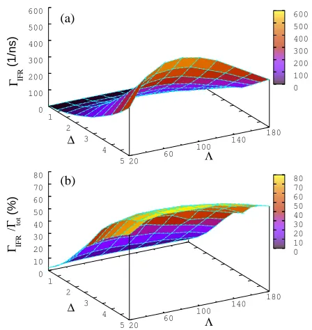
de-IFR tot IFR 0 100 200 300 400 500 600 1 2 3 4 5 20 60 100 140 180 0 100 200 300 400 500 600 0 10 20 30 40 50 60 70 80 1 2 3 4 5 20 60 100 140 180 0 10 20 30 40 50 60 70 80 (a) (b) Γ /Γ (%) Γ (1/ns) ∆ ∆ Λ Λ
FIG. 7: (Color online) Absolute (a) and relative (b) IFR scat-tering rates as a function of the IFR parameters ∆ and Λ
calculated for BF1499 atTlatt = 300 K, assuming a carrier
temperature of 320 K.
pendence owing to the temperature dependence of the hole distribution.
From Fig. 6a we see that when Tlatt increases other
mechanisms, namely acoustic and optical phonon (first the Ge-Ge and then the Si-Ge branches) and hole-hole scattering, become important. For Tlatt > 100-150
K they are comparable in magnitude to IFR, and for
Tlatt >230 K both acoustic and Ge-Ge optical phonon
scattering rates become larger than IFR rates. However from Fig. 6b we see that already for Tlatt > 70 K the
IFR contribution becomes less than 50% of the total scat-tering rate, indicating that, although still comparatively large, IFR is no longer the dominant factor influencing the subband carrier lifetimes in this temperature range. As shown in Fig. 7, at room temperature, the contribu-tion of IFR to the total scattering rate reaches 50% for ∆ = 2.5, but it is only for ∆>3.5 that such contribu-tion is above 50% for all values of 20≤Λ ≤ 180. IFR rates are however already larger than those of any other mechanism for ∆≥1.75. In contrast, we find that at low temperature (=20 K) it is only when ∆ drops below 0.6 ˚
A (i.e. for a very good quality interface), that hole-hole, alloy and acoustic phonon scattering become stronger, for most values of Λ.
[image:7.595.326.550.49.286.2] [image:7.595.76.278.49.343.2]6
scattering is dominated by IFR, one would expect the transition rates to increase with decreasing barrier width, as IFR rates are proportional to the value of the wave functions at the interface (closely related to their pene-tration into the barrier) which is larger for thinner bar-riers. The observed behaviour can however be explained by noting that the structure with the thinnest barrier (BF1499) also has the widest wells. The confinement of the wave functions is therefore reduced in BF1499 com-pared to BF1500, which would result in a reduced value at the interface if the barrier dimensions were the same. In this case the lifetime would be longer, as shown by the dashed line in Fig. 4, obtained for a hypothetical struc-ture with the wells of BF1499 and the barrier of BF1500. In the case of BF1499, however, the narrower barrier al-lows a larger penetration and the value of the wave func-tion at the interface becomes similar in both samples. This effect is well reflected by our calculated lifetimes, showing thatbothbarriersandwells need to be carefully engineered in order to tailor the intersubband lifetimes to the desired values. The effect on the lifetime of increas-ing the barrier width is obtained from a comparison of the dashed and the red lines in Fig. 4, whereas comparing the dashed and the blue lines shows the effect of widening the wells. We see that an increase of 0.5 nm in the bar-rier width is more effective in reducing the transition rate than the same increase in the width of one of the wells (and a 0.2 nm increase in the other). Further evidence that the inclusion of IFR scattering is crucial to explain the intersubband decay dynamics in SiGe heterostruc-tures is provided by the results presented in the inset of Fig. 4, where the lifetimes for BF1500 and BF1499 calculated for perfect interfaces (i.e., in the absence of IFR) are plotted as a function of lattice temperature and compared with our measured data (the same as in the mainframe). We see that both (i) the absolute values of the lifetimes of the two samples and (ii) their ratio are in plain disagreement with experiment. Point (ii) here is the most meaningful, as it clearly shows that, apart from its evidentquantitativedisagreement with our mea-surements, the observed behaviour of the lifetimes as a function of temperature cannot evenqualitativelybe de-scribed without taking into account the effects of IFR scattering. This feature excludes any possibility of at-tributing (i) to inaccuracies in our scattering calculations and suggests that the dominant role of IFR scattering in intersubband transitions, shown here for energies below the optical phonon energy in multiple quantum well sys-tems and already found in mid-infrared GaAs/AlGaAs QCLs [13], is a general property of a wide range of semi-conductor heterostructures ranging from III-V to IV-IV
materials.
V. CONCLUSIONS
In summary, we presented a theoretical and experi-mental study of the non-radiative lifetime of interwell transitions between heavy-hole subbands spaced by less than the (Ge-Ge) optical phonon energy in two differ-ent p-SiGe coupled asymmetric quantum wells. The ob-served lifetimes were found to depend on the lattice tem-perature, but showed no dependence on the excitation power over a wide range of pump intensities, indicat-ing a sub-ps intrasubband coolindicat-ing time, well below our experimental resolution. However, the reduction of the lifetimes with increasing temperature was significantly smaller than that observed in GaAs devices [2] due to the lack of polar optical phonon scattering. Our calculated transition rates included the contributions from phonon, alloy disorder, IFR and hole-hole scattering. An aver-age step height ∆ = 1.2-1.5 ˚A and a correlation length Λ = 40-60 ˚A were deduced by comparison with experi-ment, implying that our interfaces were of good quality. In spite of that we found IFR to be the strongest scat-tering mechanism up to about 200 K. In this range, vari-ations as small as 1 monolayer in the average dimensions of both barrier and wells were predicted to impact sig-nificantly on the interwell transition rates, in very good agreement with the measured data. At low temperature, IFR scattering rates were found to be larger than those of any other process for as small a step as 0.6 ˚A . By comparing our results with those obtained in a recent study [13] we concluded that, for the interface quality currently achievable experimentally in III-V and IV-IV heterostructures, IFR will dominate all other scattering mechanisms for transitions below the optical phonon en-ergy at low temperatures.
VI. ACKNOWLEDGMENTS
This work has been supported by grants from EPSRC (GR/S27528), DTI (DTI-MNT contract 491 ”Fast THz cameras using micro- and nano-technology”) and the EU project SHINE (IST-2001-38035). We also gratefully ac-knowledge support from EPSRC for the U.K. program at FELIX, from the Stichting voor Fundamenteel Onder-zoek der Materie (FOM) for providing the required beam time on FELIX. The skilful assistance by the FELIX staff was highly appreciated.
[1] F. Capasso et al., IEEE J. Quantum Electron. 38, 511
(2002).
[2] B. S. Williams, S. Kumar, H. Callebaut, Q. Hu and J. L.
Reno, Appl. Phys. Lett.83, 5142 (2003).
[3] L. Ajili et al., Appl. Phys. Lett.85, 3986 (2004).
7
Cullis, Phys. Rev. B 71, 115326 (2005); P. Murzyn, C.
R. Pidgeon, J.-P. R. Wells, I. V. Bradley, Z. Ikonic, R. W. Kelsall, P. Harrison, S. A. Lynch, D. J. Paul, D. D. Arnone, D. J. Robbins, D. Norris and A. G. Cullis, Appl.
Phys. Lett.80, 1456 (2002).
[5] S. A. Lynch, R. Bates, D. J. Paul, D. J. Norris, A. G. Cullis, Z. Ikonic, R. W. Kelsall, P. Harrison, D. D.
Arnone and C. R. Pidgeon, Appl. Phys. Lett. 81, 1543
(2002); R. Bates, S. A. Lynch, D. J. Paul, Z. Ikonic, R. W. Kelsall, P. Harrison, S. L. Liew, D. J. Norris, A. G. Cullis, W. R. Tribe and D. D. Arnone, Appl. Phys. Lett.
83, 4092 (2003).
[6] I. Bormann, K. Brunner, S. Hackenbuchner, G. Abstre-iter, S. Schmult and W. Wegscheider, Appl. Phys. Lett.
83, 5371 (2003).
[7] R. E. Prange and T. W. Nee, Phys. Rev.158, 779 (1968).
[8] H. Sakaki, T. Noda, K. Hirakawa, M. Tanaka, T.
Mat-susue, Appl. Phys. Let.51, 1934 (1987).
[9] U. Penner, H. Rucker, I. N. Yassievich, Semicond. Sci.
Technol.13, 709 (1998).
[10] T. Unuma, M. Yoshita, T. Noda, H. Sakaki, H. Akiyama,
J. Appl. Phys.93, 1586 (2003).
[11] S. Tsujino et al., Appl. Phys. Let.84, 2829 (2004).
[12] S. Tsujino et al., Appl. Phys. Let.86, 062113 (2005).
[13] A. Leuliet, A. Vasanelli, A. Wade, G. Fedorov, D.
Smirnov, G. Bastard, C. Sirtori, Phys. Rev. B73, 085311
(2006).
[14] Z. Ikoni´c, P. Harrison and R. W. Kelsall, Phys. Rev. B
64, 245311 (2001).
[15] P. C. Findlay, C. R. Pidgeon, R. Kotitschke, A. Holling-worth, B. N. Murdin, C. J. G. M. Langerak, A. F. G. van der Meer, C. M. Ciesla, J. Oswald, A. Homer, G.
Springholz, G. Bauer, Phys. Rev. B58, 12 908 (1998).
[16] Z. Ikoni´c, P. Harrison, R. W. Kelsall, J. Appl. Phys.96
6803 (2004).
[17] T. Ando, A. B. Fowler, F. Stern, Rev. Mod. Phys.54,
437 (1982).
[18] R. M. Feenstra et al., J. Vac. Sci. Technol. B 13,