Department of Engineering
PhD Thesis
Parallel diffractive multi-beam ultrafast laser
micro-processing
Thesis submitted in accordance with the requirements of The University of Liverpool for the degree of Doctor in Philosophy
By
Zheng Kuang
February 2010 Laser Group
Department of Engineering The University of Liverpool Brownlow Street
Declaration
I hereby declare that all of the work contained within this dissertation has not been submitted for any other qualification.
Signed:
Abstract
During the last decade, ultrashort pulse lasers have been employed for high precision surface micro-structuring of materials such as metals, semi-conductors and dielectrics with little thermal damage. Due to the ultra high intensity of focussed femtosecond pulses (I > 1012W/cm2), nonlinear absorption can be induced at the focus leading to highly localised material ablation or modification. This is now opening up applications ranging from integrated optics, through multi-photon induced refractive index engineering to precision surface modification for silicon scribing and solar cell fabrication.
To ensure non thermal material processing, the input fluence (F) of the ultrashort pulse laser must be kept in the low regime (F ∼ 1Jcm-2), a few times above the well defined ablation threshold. Accordingly, µJ (10-6J) level pulse energy input is often required for ultrashort pulse laser fine micro/nano-surface structuring. Running at one kilohertz repetition rate, many current ultrashort pulse laser systems can provide mJ (10-3J) level output pulse energy. Accordingly, significant attenuation of the laser output is required for many applications and hence causes a great deal of energy loss.
List of Publications to Date by Author
Peer-Reviewed Journal Publications:
Zheng Kuang, Walter Perrie, Dun Liu, S. P. Edwardson, Geoff Dearden, and K. G. Watkins, “Uniformity study of diffractive multi-beam pattern applied for parallel ultrafast laser micro-structuring” manuscript under preparation - First and corresponding author
Zheng Kuang, Dun Liu, Walter Perrie, Jian Cheng, Shuo Shang, S. P. Edwardson, E. Fearon, G. Dearden, K. G. Watkins, “Diffractive Multi-beam Ultra-fast Laser Micro-processing Using a Spatial Light Modulator(Invited paper)”, Chinese Journal of Lasers, Vol. 36, No. 12, pp. 3093 – 3115, (2009) - First author
Zheng Kuang, Walter Perrie, Dun Liu, Stuart Edwardson, Jian Cheng, Geoff Dearden and Ken G. Watkins “Diffractive multi-beam surface micro-processing using 10 ps laser pulses”, Applied Surface Science, Vol. 255, Issue 22, pp. 9040 – 9044 (2009) –
First and corresponding author
Zheng Kuang, Dun Liu, Walter Perrie, Stuart Edwardson, Martin Sharp, Eamonn Fearon, Geoff Dearden and Ken G. Watkins, “Fast parallel diffractive multi-beam femtosecond laser surface micro-structuring” Applied Surface Science, Vol. 255, Issues 13-14, pp. 6582-6588, (2009) – First and corresponding author
Conference Publications:
Z. Kuang, D. Liu, W. Perrie, J. Cheng, S. P. Edwardson, G. Dearden, and K. G. Watkins, “Fast parallel diffractive multi-beam laser surface micro-structuring” Paper No: 1782 – 36th MATADOR Conference – First author
Z. Kuang, D. Liu, W. Perrie, J. Cheng, S. Shang, S. P. Edwardson, E. Fearon, G. Dearden, and K. G. Watkins, “Multiple beam ultrafast laser microprocessing (Invited paper)”, PICALO Congress Proceedings (M103), March 23 – 25, 2010 - First author
D. Liu, Z. Kuang, S. Shang, W. Perrie, D. Karnakis, A. Kearsley, M. Knowles, S. Edwardson, G. Dearden and K. G. Watkins, “Ultrafast parallel laser processing of materials for high throughput manufacturing” Proceeding of LAMP 2009 – The 5th International Congress on Laser Advanced Materials Processing – Co-author
Z. Kuang, W. Perrie, M. Sharp, S. P. Edwardson, G. Dearden and K. G. Watkins, "Diffractive Multi-Beam Ultra Fast Laser Processing by Using a Spatial Light Modulator", IOP Photon08 Conference, 26-29 August 2008 – First author/Presenter
Acknowledgements
First of all, I hereby sincerely acknowledge my supervisors, Professor Ken Watkins and Dr Geoff Dearden at the Laser Group of the University of Liverpool, who offered support, guidance and encouragement throughout this research. Without their kind and solid dedication, this paper would not have been possible. I also owe much to Dr Walter Perrie, a senior researcher at our Laser Group, whose insights into ultrashort pulse laser material processing have helped me to accomplish this thesis successfully.
At the same time, I am also thankful for the professional instruction and effective assistance from other members in our research group: Dr Stuart Edwardson, Dr Martin Sharpe and Dr Eamonn Fearon, and appreciate all the kind help from my fellow students: Leigh Mellor, Olivier Allegre, Dun Liu, Jian Cheng and Spencer Shang, who always show me a good sample of working under any hard situation.
I also gratefully acknowledge Prof. Miles Padgett and Dr. Jonathan Leach at University of Glasgow for giving kind help on the hologram calculation used for this research.
Additionally, I would like to thank the Scholarship of Overseas Research Students Award Scheme (ORSAS) and the Scholarship of University of Liverpool Graduate Association (Hong Kong) for providing financial support for my PhD study at the University of Liverpool.
Table of Contents
Abstract
III
List of Publications to Date by Author
IV
Acknowledgements
VI
Table of Contents
VII
List of Figures
XII
List of Tables
XXII
List of Symbols XXIII
List of Abbreviations
XXV
Chapter 1 – Introduction
1.1 Background to research area ... 2
1.2 Motivation... 3
1.3 Overview of the thesis ... 5
Chapter 2 – Literature Review
2.1 Introduction ... 82.2 Ultrashort pulse laser systems and ultrashort pulse laser material processing ... 8
2.2.1 Ultrashort pulse laser systems ... 8
2.2.1.1 Emission spectrum of the active medium... 8
2.2.1.2 Chirped pulse amplification (CPA)... 9
2.2.1.3 Simple and compact picosecond laser system ...13
2.2.2 Ultrashort pulse laser ablation of material ...15
2.2.2.1 Absorption of laser energy ...16
2.2.2.2 Well defined ablation threshold with ultrashort pulses...17
2.2.2.4 Material processing with picosecond laser pulses ...22
2.2.3 The limitations of ultrashort pulse laser processing ...25
2.3 Multiple beam parallel processing ... 27
2.3.1 Parallel microfabrication of periodic structures ...28
2.3.2 Parallel microfabrication of arbitrary structures...32
2.4 The generation of multiple beams using a spatial light modulator (SLM)... 34
2.4.1 Introduction to SLM technology ...34
2.4.2 Generation of multiple beams with an SLM ...39
2.5 The calculation of Computer Generated Hologram (CGH) algorithms ... 41
2.5.1 CGH calculation algorithms summary...41
2.5.1.1. Algorithms for calculating Fourier Plane Holograms...41
2.5.1.2. Multiplexing Phase Fresnel Lenses (MPFL) algorithm for calculating Fresnel Plane Holograms ...49
2.5.2 Calculation of CGHs with a LabVIEW program ...52
2.6 Summary ... 54
Chapter 3 – Experimental Equipment and Techniques
3.1 Introduction ... 573.2 Principal experimental apparatus used for the research ... 57
3.2.1 Ultrashort pulse laser systems ...57
3.2.1.1 Clarke-MXR CPA2010 femtosecond laser system...57
3.2.1.2 High-Q picoseconds laser system ...60
3.2.2 Spatial Light Modulators (SLM) ...62
3.2.2.1 Boardband coated SLM – Holoeye...62
3.2.2.2 Dielectric coated SLM – Hamamatsu ...63
3.2.2.3 High power tests on Spatial Light Modulators (SLM)...64
3.2.3 Scanning galvanometer systems and multi-axis motion control systems...69
3.2.3.1 Scanning galvanometer systems ...69
3.2.3.2 Multi-axis motion control system (Aerotech) ...71
3.3 Methods to remove the zero order beam ... 72
3.3.1 Removal of the zero order beam with a 4f-imaging optical system ...73
3.3.1.2 Modelling the 4f-imaging optical system with ZEMAX ...75
3.3.2 Removal of the zero order beam by adding a Fresnel zone lens ...78
3.3.2.1 Defocusing of the zero order beam at processing plane ...78
3.3.2.2 Combination of the Fourier and Fresnel plane hologram ...82
3.4 Experimental setup ... 82
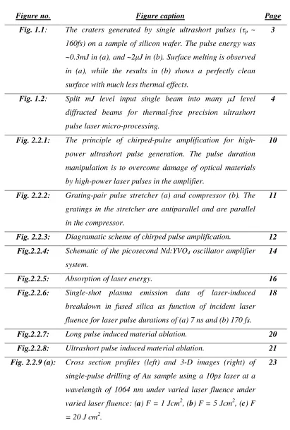
3.4.1 Experimental setup without the 4f optical system...83
3.4.2 Experimental setup with 4f optical system ...84
3.5 Summary ... 86
Chapter 4
-Diffractive multi-beam microprocessing using
femtosecond laser pulses
4.1 Introduction ... 884.2 Static CGH multiple laser beam micro-processing ... 88
4.2.1 Precision micro-drilling using diffractive µJ-level multiple beams ...88
4.2.2 The distortion of beam shape caused by finite spectral bandwidth...94
4.2.2.1 The observation of distorted beam shape ...94
4.2.2.2 Prediction of the eccentricity of beam shape by calculation ...97
4.2.2.3 Effect of beam shape distortion on process stability...98
4.3 Laser microprocessing with dynamic diffracted beam patterns... 99
4.3.1 Response time of the SLM ...99
4.3.2 Micro-processing by real time playing CGHs...102
4.3.3 Synchronizing the action of hologram application with scanning techniques ...105
4.4 Summary ...107
5.2 Experimental setup ...109
5.3 Spectral bandwidth effect on diffracted beam shape...110
5.4 High power parallel processing with high repetition rate at f =20kHz ...113
5.5 Summary ...114
Chapter 6 - Uniformity study of diffractive laser beam patterns
6.1 Introduction ...1176.2 Methodology of the uniformity study...118
6.2.1 Geometric design of the diffractive pattern ...118
6.2.2 The uniformity measurement ...119
6.3 Results of uniformity study...120
6.3.1 Diffraction efficiency and uniformity resulting from the geometric pattern design...120
6.3.2 Generating symmetric patterns by combination of several asymmetric pattern with good uniformity...123
6.4 Discussion ...126
6.4.1 The degeneracy of the design pattern ...126
6.4.2 Degeneracy avoided by adding a random phase ...127
6.5 Summary ...128
Chapter 7 - Investigations into potential applications of diffractive
multiple beam laser microprocessing
7.1 Introduction ...1307.2 High throughput surface micro-structuring of silicon ...130
7.2.1 Diffractive multi-beam pattern design ...131
7.2.2 Results of micro-structuring of silicon using the diffractive patterns ...132
7.3 Laser patterning of organic light emitting diode (OLED) materials ...134
7.3.1 Diffractive multi-beam patterning of cathode layers...135
7.4 Selective ablation of surface material (silicon wafer) by diffractive multi-beams
...137
7.4.1 Selective ablation by modulating the focal height...137
7.4.2 Multi-beam scanning with different number of spots per line ...140
7.5 Diffractive multi-beam internal structuring of volume gratings ...141
7.5 Summary ...144
Chapter 8 - Conclusions and recommendation for future work
8.1 Conclusions...1468.2 Recommendation for Future Work...148
References
…………..……….…………..151
List of Figures
Figure no. Figure caption Page
Fig. 1.1: The craters generated by single ultrashort pulses (τp ~
160fs) on a sample of silicon wafer. The pulse energy was ~0.3mJ in (a), and ~2µJ in (b). Surface melting is observed in (a), while the results in (b) shows a perfectly clean surface with much less thermal effects.
3
Fig. 1.2: Split mJ level input single beam into many µJ level diffracted beams for thermal-free precision ultrashort pulse laser micro-processing.
4
Fig. 2.2.1: The principle of chirped-pulse amplification for high-power ultrashort pulse generation. The pulse duration manipulation is to overcome damage of optical materials by high-power laser pulses in the amplifier.
10
Fig. 2.2.2: Grating-pair pulse stretcher (a) and compressor (b). The gratings in the stretcher are antiparallel and are parallel in the compressor.
11
Fig. 2.2.3: Diagramatic scheme of chirped pulse amplification. 12 Fig.2.2.4: Schematic of the picosecond Nd:YVO4 oscillator amplifier
system.
14
Fig.2.2.5: Absorption of laser energy. 16
Fig.2.2.6: Single-shot plasma emission data of laser-induced breakdown in fused silica as function of incident laser fluence for laser pulse durations of (a) 7 ns and (b) 170 fs.
18
Fig.2.2.7: Long pulse induced material ablation. 20 Fig.2.2.8: Ultrashort pulse induced material ablation. 21 Fig. 2.2.9 (a): Cross section profiles (left) and 3-D images (right) of
single-pulse drilling of Au sample using a 10ps laser at a wavelength of 1064 nm under varied laser fluence under varied laser fluence: (a) F = 1 Jcm2, (b) F = 5 Jcm2, (c) F = 20 J cm2.
Fig. 2.2.9 (b): Cross section profiles (left) and 3-D images (right) of single-pulse drilling of Au sample by using a 180 fs laser at a wavelength of 775 nm under varied laser fluence: (a) F = 1 J cm−2, (b) F = 5 Jcm−2, (c) F = 10 J cm−2.
24
Fig. 2.2.10: Single shot femtosecond ablation of polished aluminium, where F ≈ 14J/cm2 (a), F ≈ 14J/cm2 (b).
26
Fig. 2.3.1: Experimental design of material parallel processing using the method of multi-beam interference.
28
Fig. 2.3.2: Calculated intensity profiles of 2D periodic patterns. 29 Fig. 2.3.3: Scanning electron microscopy (SEM) images of the
structure fabricated by the multi-beam interference of ultrashort pulses. (a) Top view, (b) oblique view of the same sample, and (c) oblique view of another sample fabricated at larger exposure energy.
30
Fig. 2.3.4: Basic scheme of optical setup. MLA: microlens array, L1: lens, DM: dichroic mirror, OL: objective lens. A is the plane where multiple foci are generated
31
Fig. 2.3.5: An optical micrograph of the fabricated structure by MLA laser processing.
31
Fig. 2.3.6: The results showing the microstructuring using a DOE generated arbitrary multi-beam pattern. (a) The designed focal shape of the pattern, (b)The modulated beam profile, (c) Surface view of ablation pattern observed by optical microscopy, (d) Processed are inside the glass observed by optical microscopy, left: top view, right: side view.
32
Fig. 2.3.7: Experimental setup of the holographic femtoseond laser processing system.
33
Fig. 2.3.8: (a) A target pattern for calculating a CGH, (b) the calculated CGH, (c) the computational reconstruction of the CGH, (d) the optical reconstruction of the CGH at the plane P, (e) a transmission microscope image, and (f) an Atomic Force Microscopy (AFM) image of the fabricated
area. The vertical scale of the AFM profile is ±500 nm.
Fig. 2.4.1: The sketches demonstrate different types of SLM, reflective (a) & transmissive (b), and how they work.
35
Fig.2.4.2: The basic structure of LCD. 36
Fig. 2.4.3: The measured results from a Holoeye LC-R 2500 SLM with
λ = 632.8nm linearly polarized laser input, showing a near linear increase of the phase modulation with increasing the grey level (from 0 to 255).
37
Fig. 2.4.4: The setup for intensity modulation 38 Fig.2.4.5: How an SLM works - modulate the phase/intensity of the
light
38
Fig. 2.4.6 (a): Creation of multiple beams with Fourier Plane Hologram. 39 Fig. 2.4.6 (b): Creation of multiple beams with a Fresnel Plane
Hologram
40
Fig. 2.4.6 (c): Creation of multiple beams with the third type of hologram, of the Fourier and Fresnel plane hologram
41
Fig. 2.5.1: Fourier relationship between the plane of the hologram and the image space of the focal lens.
43
Fig. 2.5.2: The diagram graphically shows how to generate phase hologram with the GS Algorithm
45
Fig.2.5.3: Phase required for lateral and axial shifts. 46 Fig. 2.5.4: 2D arbitrary multiple laser beam pattern generated by
complex superposition of prism phases
47
Fig 2.5.5: Fresnel (near field) diffraction and Fraunhofer (far field) diffraction
50
Fig. 2.5.6: Comparison of the reconstructive plane of multiple foci using Fourier (a) and Fresnel (b) plane hologram
51
Fig.2.5.7: The interface of the LabVIEW program generated by Leach et al.
53
Fig.2.5.8: A CGH calculated by the program (a) and its computational reconstruction (b).
54
Fig. 3.2.3: Schematic of the fibre oscillator. WP denotes waveplates and BRF denotes birefringent filter
59
Fig. 3.2.4: High-Q IC-355-800ps picosecond laser system 60 Fig. 3.2.5: The interface of High-Q IC-355-800ps control software 61 Fig. 3.2.6: Commercial SLMs used for current research: (a )Holoeye
LC-R 2500, (b) Hamamatsu X10468-03 (X10468-04 has the same appearance of X10468-03).
62
Fig. 3.2.7: Experiment setup for high power laser beam test on the SLMs
65
Fig. 3.2.8: Variation in intensity with grey level, detected when uniform images are displayed onto the X10468-03 Hamamatsu SLM.
67
Fig. 3.2.9: The change of detected relative intensity, In / Imax, versus
the time after the illumination. The blue data is from X10468-03 SLM with high reflectivity dielectric coating, while the red data is from LC-R 2500 absorbing more thermal energy due to its lower reflectivity.
68
Fig. 3.2.10: The workings of the galvanometer driven laser beam scanning system, which consists of two galvanometer driven mirrors (X and Y), a flat field f-theta lens with focal length f ≈ 100mm, and integrated driver electronics enclosed in a black cube-like metallic case.
70
Fig. 3.2.11: The interface of the software used to control the scanning galvanometer system.
71
Fig. 3.2.12: Four axis (a) and five axis (b) Aerotech motion control systems used for current research
72
Fig. 3.3.1: An ‘LLEC’ pattern with 32 desired diffracted beams projected on a paper screen.
73
Fig. 3.3.2: Schematic diagram for blocking the zero order beam at the Fourier plane P of the 4f optical system
74
Fig. 3.3.3: 3D layout of the modeled 4f optical system 76 Fig. 3.3.4: Spot diagram showing each spot size on the mirror – The
radius of the spots, r, is given beneath; the energy
intensity, I, hence was easily calculated by I Ep2 r π
= , which
was well below the damage threshold of the mirror coating.
Fig. 3.3.5: Demonstration of the enhancement of the +1 diffracted orders (LLEC pattern) combined with blocking the zero order beam using a small metallic target. The image shows intensity distribution on a paper screen taken with a digital camera.
78
Fig. 3.3.6: Interface of the software developed by Holoeye, which can easily superimpose and adjust the phase of the PFL.
79
Fig. 3.3.7: Schematic showing the method to separate the focal plane of diffracted beams from the zero order beam. The added PFL, lens 1, can work as either positive lens (upper) or negative lens (lower) to obtain the separation, ∆d. The beam matrix equation describes the propagation of diffracted beam from LCoS surface (A) to its focal plane (B)
81
Fig. 3.3.8 (a): A CGH calculated by GL algorithm to generate eight first order identical beams (left) and its computational reconstruction (right)
81
Fig. 3.3.8 (b): The CGHs superimposed by PFLs with different f1 to adjust
∆d (upper) and the machined results on Ti6Al4V (lower)
82
Fig. 3.4.1: Experiment setup without the 4f optical system 83 Fig. 3.4.2: The schematic of experiment setup for Clark-MXR
CPA2010 with a 4f optical system
84
Fig. 4.2.1 (a): ‘LLEC’ pattern comprising 32 micro-sized holes 89 Fig. 4.2.1 (b): Random spots pattern comprising 30 micro-sized holes 89
Fig. 4.2.2: Hole size and eccentricity versus the distance from each diffracted spot to the zero order hole in both ‘LLEC’ and random spots patterns
91
Fig. 4.2.3: The zero orders removed when micro-structuring a silicon substrate with the ‘LLEC’ and random spots patterns.
Fig. 4.2.4 (a): Illustration of how the desired +1 diffractive beam retains a round shape when the input beam has a single wavelength i.e. ∆λ→ 0.
94
Fig. 4.2.4 (b): Illustration of how the shape of desired +1 diffractive beam is elongated towards zero order beam when the input beam has a measurable finite bandwidth, ∆λ≈ 5nm.
95
Fig. 4.2.5 (a): Observed growing eccentricity of micro-machined holes on a silicon substrate with increasing diffractive angle of +1 orders, showing a slight tilt of the major axis. The ablation debris is deposited non-uniformly due to the asymmetric expansion of the plasma. The zero order is marked.
96
Fig. 4.2.5 (b): Improved result over figure 4.2.5 (a) in which the major axis of the elliptical structures aligns to the zero order. The debris has been simply removed using methanol.
96
Fig. 4.2.6: Experimental and calculated eccentricity a/b of machined holes versus angle of diffraction showing excellent agreement. Eccentricity increases linearly with angle of diffraction.
98
Fig. 4.2.7: A comparison of ablation depth on Ti6Al4V with angle of diffraction and pulse number, showing that the ablation depth drops at higher angles due to increasing distortion of the intensity profile.
99
Fig.4.3.1: Optical micrograph of the machined pattern on a silicon wafer, where the CGH1 was fading out and CGH2 was building up during the scanning. The number of zero order beam machined holes between A and B was 27, and the period of time between two adjacent holes was 1ms; hence the response time was estimated at ~ 27ms.
101
Fig. 4.3.2: Rise and fall times of SLM (LC-R 2500) given by Holoeye. 101 4.3.3 (a): Pattern completed by real time playing 15 series of CGHs
at 20 Hz refresh rate (50ms duration per CGH).
103
[image:17.612.98.515.60.730.2]control with Galvanometer scanning
Fig. 4.3.5: ‘OPTICS’ pattern created by 7 CGHs applied at appropriate positions using the galvanometer scanner (shown together with zero order holes)
106
Fig. 4.3.6: ‘OPTICS’ pattern with zero order holes eliminated (The insert 3D pictures were measured using Wyko NT1100 optical surface profiler, illustrating the depth of the holes)
106
Fig. 5.2.1: Schematic of experiment setup for High-Q IC-355-800ps with a 4f optical system
109
Fig. 5.3.1: (a) A series holes drilled on a silicon sample when varying the diffractive angle. (b) The 2D (left) and 3D (right) micrographs with large magnification, showing the shape of the hole, fabricated by single 10ps pulse, when applying large diffractive angle, θ > 1°
111
Fig. 5.3.2: The eccentricity e of hole shape drilled by 10ps when varying the angle of diffraction.
112
Fig. 5.3.3: The variation of ablation depth using one thousand 10ps pulses (Ep ≈ 5µJ) when varying the angle of diffraction.
112
Fig. 5.4.1: Schematic showing the design of the 25 beams pattern and the method of scanning (The vertical distance between two adjacent spots was 100µm; by repeatedly scanning the pattern with 50µm vertical offset each time, multiple micro-channels with 50µm intervals can be obtained.)
113
Fig. 5.4.2: Micrograph demonstrating the results of micro-channels covering a 10 × 10mm area machined by the 25 beams pattern on polished Ti6Al4V (upper), and micrographs showing the result with higher magnification (lower left) and 3D surface profile image by Wyko NT1100 optical surface profiler (lower right)
114
Fig. 6.2.1: The periodic 5×5 array with high degree of symmetry - the basic geometric design of a diffractive pattern
118
Fig. 6.2.2: Schematic showing that by applying a freedom of asymmetry, R, the position of each desired diffractive
peaks is no longer fixed, but randomly located within a circle area.
Fig. 6.3.1: The optical micrographs demonstrating the machining results on a polished Ti6Al4V substrate using LG algorithm when the freedom of asymmetry was set to be: R = 2 µm, 20 µm, 50 µm. Clearly, the pattern with high degree of symmetry, shows poor uniformity, e.g. When R =2 µm, V ≈ 41.2%, while more asymmetrically designed pattern has good uniformity, e.g. When R =50 µm, V ≈
5.6%
121
Fig. 6.3.2 (a): The diffractive efficiency of the multi-beam pattern versus the freedom of asymmetry, R
122
Fig. 6.3.2 (b): The uniformity of the machined holes on a Ti6Al4V substrate (described by the Percentage of Variation) versus the freedom of asymmetry, R
122
Fig. 6.3.3 (a): The design of a 10×4 hole array pattern formed by four asymmetric patterns.
123
Fig. 6.3.3 (b): The processing results of 10×4 holes array pattern with (left) and without (right) zero order holes
124
Fig. 6.3.3 (c): The result produced by repeating the patterns with the galvanometer system to create large area processing.
125
Fig. 6.3.3 (d) and (e):
Schematic showing the combination of the four asymmetric patterns used to a generate 3D chessboard-like structure (d) ,and the micro-machined 3D chessboard structure(e)
125
Fig. 6.4.1: A digital camera photograph showing a diffractive pattern reconstructed on a paper screen – Only the four brighter spots marked by a blue triangle are the desired diffractive orders, all the other weaker spots appearing on the dark background are the ghosts. The red dashed line marks a series spots generated by a phase grating, where only the +1 order is desired.
126
Fig. 6.4.2: N×M beams array 127
silicon – generating a 10×4 beam array
Fig. 7.2.2: Scanning patterns for six concentric circles. (a) d = 0.3mm; no interference among the scanned circles, (b) d = 0.2mm; partial interference among the scanned circles, (d) d = 0.15, total interference among the scanned circles.
132
Fig. 7.2.3: Change of the contact angle versus the surface morphology (controlled by d) and chemistry (before and after the oxidised layer removed)
134
Fig. 7.3.1: The layered structure of OLED material. 135 Fig. 7.3.2: Parallel processing of OLED. Optical micrographs
(Upper), cross-sectional profile of a single line (bottom)
136
Fig. 7.3.3: Parallel processing of ITO thin film sample using a diffractive multi- beam. Top: Optical micrographs; Bottom: Cross-sectional profile of a single scribe
137
Fig. 7.4.1: (a) The CGH, calculated by 3D Gershberg-Saxton algorithm, which can create a ‘NWDA’ diffracted beam pattern with 39 multiple beams focused at two different planes. (b) Schematic showing the computationally reconstructed ‘NWDA’ pattern.
138
Fig. 7.4.2: Processing result for the ‘NWDA’ pattern applied to a polished Ti6Al4V sample
139
Fig. 7.4.3: Schematic demonstrating the size of hole adjusted by precisely modulating the focal height difference of each diffractive order, ∆d. (a) The diffractive beam is precisely focused on the sample surface hence fabricating a larger sized hole; (b) the diffractive beam is slightly out of focus by a distance (∆d), hence fabricating smaller sized hole.
140
Fig. 7.4.4 (a): Schematic of selective ablation using different number of spots per line to produce different ablation depth.
140
Fig. 7.4.4 (b): Micrograph of 10 beams selective ablation on silicon. The red circles represent the positions of the 10 beams.
140
Fig. 7.4.4 (c): Cross-sectional surface profile of the 10 beams selective ablation on silicon. The scribe line 1, 2, 3 and 4 are
consistent with those labeled in Fig. 7.2.4 (b)
Figure 7.5.1: Schematic showing internal volume grating fabrication by applying parallel processing of diffractive multi-beam.
142
Fig. 7.5.2: Top: digital camera picture showing a series of volume gratings written inside a PMMA slab. Bottom: high magnification micrograph showing the fabricated grating with period, T ≈ 19µm.
142
Figure 7.5.3: Schematic showing the diffracted pattern of 21 desired beams, as applied to fabricate a volume grating at a scanning at a speed of 1mm/s
143
Fig. 8.2.1: Selective ablation of multi-layer structured material using a diffractive multi-beam pattern
List of Tables
Table no. Table caption Page
Table 3.1: Specifications of SLMs employed for present research 64 Table 3.2: The details of lens chosen for building up the 4-f optical
system
75
Table 3.3: Optimized value of distance between each optical element to minimize the wavefront distortion
77
Table 4.1: The calibrated series of drilled holes diameter using a single beam of varying pulse energy
90
Table 7.1: The results of micro-structuring of silicon using the diffractive multi-beam patterns
List of Symbols
Symbol Unit Description
a (µm) Major semiaxis of ellipse A n/a Amplitude of complex field b (µm) Minor semiaxis of ellipse
Ce (J·kg-1·K-1) Specific heat capacity of electron
Cl (J·kg-1·K-1) Specific heat capacity of lattice
D n/a Heat diffusion coefficient e n/a Eccentricity of the hole shape E(t), E(r) n/a Electric field
Ep (µJ) Pulse energy
f (mm) Focal length
F (J·cm-2) Laser fluence
FT n/a Fourier transform
g (W·m-3·K-1) Electron-phonon coupling constant
G n/a Gain factor
I (W·cm-2) Intensity
k n/a Wave number
L (µm) Ablation depth per pulse ld (µm) Heat diffusion length
ls (µm) Optical penetration skin depth
n n/a Refractive index
NA n/a Numerical aperture
R (Hz) Repetition rate
t K Temperature
Te K Temperatures of electrons
Tl K Temperatures of lattice
X (µm) Distance of the beam from the axis
Symbol Unit Description
∆d (mm) Separation of focal planes ∆l (µm) Elongation of the hole shape
∆n n/a Refractive index change
∆λ (nm) Spectral bandwidth
δ n/a Optical path difference
η n/a Diffraction efficiency
θi (º) Incident angle
θm (º) m-th order diffractive angle
κe (W·K−1·m−1) Electron thermal conductivity
λ (nm) Wavelength
Λ (µm) Grating period
ν (Hz) frequency
τp (fs or ps) Pulse duration (pulsewidth)
φ n/a Phase of complex field
Φ (µm) Hole diameter
ψ a/n Complex field representing the laser beam
List of Abbreviations
Abbreviations Full names
3D Three dimension
AR. coating Anti-reflection coating BBO crystal Beta-barium borate crystal
CCD Charge-coupled device
CGH Computer generated hologram
CPA Chirped pulse amplification
DVI Digital visual interface
ER-SLM Electrically addressed reflective SLM
FWHM Full-width at half-maximum
GS algorithm Gerchberg-Saxton algorithm
IR Infrared
ITO Indium tin oxide
LC Liquid crystal
LCoS Liquid crystal on silicon LG algorithm Lenses and gratings algorithm LLEC Lairside laser engineering centre MEMs Microelectromechanical systems
MPFL algorithm Multiplexing phase fresnel lenses algorithm
NIR Near Infrared
NWDA Northwest regional development agency OLED Organic light emitting diode
PFL Phase Fresnel lens
PMMA Poly(methyl methacrylate)
SLM Spatial light modulator
UV Ultra-violet
Chapter 1
1.1 Background to research area
During the last decade, ultrashort pulse lasers have been employed for high precision surface micro-structuring of materials such as metals, semi-conductors and dielectrics with little thermal damage. Due to the ultra high intensity of focussed femtosecond pulses (I > 1012W/cm2), nonlinear absorption can be induced at the focus leading to highly localised material ablation or modification. This is now opening up applications ranging from integrated optics, through multi-photon induced refractive index engineering to precision surface modification for silicon scribing and solar cell fabrication.
However, experimental results have demonstrated that significant thermal effects still occur during material processing with the ultrashort pulses when high pulse energy is applied. To ensure non thermal material processing, the input fluence, F, must be kept in the low regime (F ∼ 1Jcm-2), a few times above the well defined ablation threshold. Accordingly, µJ (10-6J) level pulse energy input is often required for ultrashort pulse laser fine micro/nano-surface structuring.
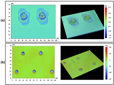
Figure 1.1 (a) and (b) show the single pulse (τp ~ 160fs) machined craters with
Fig. 1.1: The craters generated by single ultrashort pulses (τp ~ 160fs) on a sample of
silicon wafer. The pulse energy was ~0.3mJ in (a), and ~2µJ in (b). Surface melting is observed in (a), while the results in (b) shows a perfectly clean surface with much less
thermal effects.
1.2 Motivation
Running at one kilohertz repetition rate, many current ultrashort pulse laser systems can provide mJ (10-3J) level output pulse energy. Accordingly, significant attenuation of the laser output is required for many applications and hence causes a great deal of energy loss.
systems operating at much higher frequencies, above 100kHz can hit speed limitations on scanners while much more care is required in terms of pulse gating and synchronisation.
Generating multiple beams, spatially splitting a mJ level energy laser pulse into many
µJ laser pulses required for high quality non-thermal micro-machining, is another method to increase the efficiency and throughput of ultrashort pulse laser processing. From multiple-beam interference to micro-lens arrays, previous studies have demonstrated many approaches to create multiple beams to improve ultrashort pulse laser micro-fabrication. In order to generate arbitrary multiple beam patterns, being able to attempt parallel processing flexibly and variably, the Spatial Light Modulator (SLM) which is a powerful device of dynamic diffractive optical elements (DOE) has been employed for multiple beam generation, as shown in figure 1.2. However, due to the complicated experimental alignment, the processing is not sufficiently flexible to reach industrial requirement. Additionally, the uniformity of multiple beams is problematic, which can significantly degrade the machining quality.
Fig. 1.2: Split mJ level input single beam into many µJ level diffracted beams for
With these limitations in mind, the present study uses an SLM allowing mJ pulse energy input to variably create > 30 uniform multiple beams with the demonstration of addressing CGHs in real time and synchronizing with a scanning method, which adds a great flexibility for material micro-processing. Furthermore, the uniformity of multiple beams is studied in this thesis, which gives some solutions of generating multi-beam patterns with a high uniformity.
With the high throughput gain and the great processing flexibility, the result shows many potential applications, such as fabrication of hydrophobic biomimetic surfaces with a self-cleaning ability, surface micro-structuring of metals or silicon wafers (the materials for Microelectromechanical systems (MEMS) manufacturing), and laser patterning of multi-layer structured materials, e.g. Organic Light Emitting Diode (OLED) and thin film solar cells.
1.3 Overview of the thesis
The thesis consists of eight chapters. The current chapter (Chapter 1) is the main introduction of the thesis.
Chapter 2 is the literature review. The relevant background knowledge, ranging from a brief introduction of ultrashort pulse laser systems, ultrashort pulse induced material processing to a review of the diffractive multi-beam generation method using an SLM, is reviewed in this chapter.
Chapters 4 to 7 are the results and discussion section of the thesis. First of all, Chapter 4 focuses on the diffractive multi-beam microprocessing using femtosecond laser pulses, where the results demonstrate great gains in processing throughput and flexible surface structuring by applying holograms in real time while synchronising the scanning galvanometer. However, chromatic distortion of the beam shape is observed due to the broad spectral bandwidth of the laser source. Accordingly, picosecond laser pulses with much narrower bandwidth are employed for parallel processing as described in Chapter 5. The results not only demonstrate negligible chromatic distortion, but also faster processing speed with higher repetition rate. Then, Chapter 6 describes a study of diffractive pattern uniformity, which significantly affects the reproducibility of processing. Finally, potential applications are demonstrated in Chapter 7. Finally, Chapter 8, Conclusions and future work, is the last part of the thesis.
Chapter 2
2.1 Introduction
This chapter will review the background knowledge of current research. Ultrashort pulse laser systems and ultrashort pulse laser microprocessing of materials will be introduced. One of the main drawbacks of ultrashort pulse laser material processing is the low processing efficiency and throughput. Overcoming this limitation of ultrashort pulse laser processing by creating multiple beams with a Spatial Light Modulator (SLM) is the main purpose of this research. In the following sections of this chapter, different methods of generating multiple beams will be discussed by reviewing the relevant literature.
2.2 Ultrashort pulse laser systems and ultrashort pulse laser material
processing
2.2.1 Ultrashort pulse laser systems
2.2.1.1 Emission spectrum of the active medium
In order to generate an ultrashort pulse in a laser oscillator, the laser active medium, the fundamental requirement for an ultrashort pulse laser, must have a broad, continuous emission spectrum. This is due to the principle that the Fourier-transform-limited laser pulse duration is inversely proportional to its spectral width,
constant
p
τ ⋅ ∆ν = (2.2.1)
where τpis the pulse duration and ∆ν is the pulse frequency spectrum, both measured
at Full-Width at Half-Maximum (FWHM) [2-4]. For a Gaussian pulse, whose electrical field amplitude is given by:
2
0 0 2
( ) exp( 2 ) exp( 2 ln 2 )
p
t
E t E πν t
τ
= − − (2.2.2)
2 0
0 2
( )
( ) FT{ ( )} 'exp[ 2 ln 2 ]
Eν E t E ν ν
ν −
= = −
∆ (2.2.3)
and:
2 ln 2 0.44
p
τ ν
π
⋅ ∆ = ≈ (2.2.4)
To meet this fundamental requirement, Ti:sapphire, which has an emission spectrum that can support pulses down to ~ 6fs, has been widely chosen by researchers and commercial ultrashort pulse laser manufacturers to be the ultrashort pulse laser active medium. Other ultrashort pulse laser active media include: dyes, Cr:LiSAF, Nd:glass, Yb:glass, Yb:YAG, and Cr:YAG.
With a suitable laser active medium, ultrashort pulses are generated in a mode-locked oscillator, which can be accomplished either by Kerr-lens mode locking [5], additive pulse mode locking [6], or a special solid-state passive saturable absorber [7, 8]. Furthermore, dispersion in the optical materials (i.e. different frequency components of the pulse travel at different speeds) may stretch out the short pulse with broad spectral bandwidth, ∆ν, in the active medium and other optical elements in the cavity, termed pulse spreading. Therefore, in addition to mode locking, the ultrafast oscillator has to compensate pulse spreading by inserting an optical component with dispersion opposite to the optical active medium into the oscillator. This component is usually made of a prism pair [9, 10] or specially designed chirped mirrors [11, 12].
2.2.1.2 Chirped pulse amplification (CPA)
The ultrashort pulse laser oscillator usually operates at a pulse repetition rate of approximately 100 MHz, giving the pulse energy, Ep, in the range of nanojoules (nJ).
hence amplification to the millijoule (mJ) level is necessary. The pulses cannot be amplified directly, as the optical components inside the amplifier will be damaged by the high intensity level of the short pulses; furthermore, the effect of self-focusing associated with high-intensity pulses can make the situation worse.
Fig. 2.2.1: The principle of chirped-pulse amplification for high-power ultrashort pulse generation. The pulse duration manipulation is to overcome damage of optical
materials by high-power laser pulses in the amplifier.
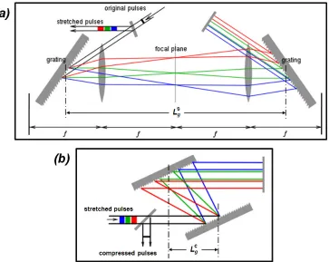
Fig. 2.2.2: Grating-pair pulse stretcher (a) and compressor (b). The gratings in the stretcher are antiparallel and are parallel in the compressor. [16]
The pulse stretcher and compressor are normally made of a pair of optical gratings [14]. Figure 2.2.2 (a) demonstrates one implementation of the grating stretcher [15, 16]. The dispersive properties of the gratings are exploited to change the pulse duration of an ultrashort pulse having broad frequency spectral bandwidth, ∆ν, and the pulse is stretched while travelling between the pair of optical gratings. Different frequency components in the pulse are dispersed into different directions each time reflected on the gratings; hence they have different optical path lengths. Consequently, the frequency component that has a shorter optical path length will come out earlier than the frequency component that travels a longer path, hence the pulse is stretched. The amount of stretching is determined by the distance, Ls = 4f - Lgs, where Lgs is the
The compressor, demonstrated in Figure 2.2.2 (b), is also made of a pair of gratings, but the dispersion is arranged in the opposite way as the stretcher. The amount of compression is simply determined by the separation of the grating-pair, Lc = Lgc. To
obtain the shortest compressed pulse, the compressor and the stretcher must match so that Lc = Ls. Pulse duration other than the shortest can be easily obtained by simply
[image:37.612.128.484.298.527.2]misaligning the compressor to the stretcher by varying the grating separation. Figure 2.2.3 schematically shows a chirped pulse amplification system with grating-pair pulse stretcher and compressor.
Fig. 2.2.3: Diagramatic scheme of chirped pulse amplification [16]
short laser pulses at 10ps with much narrower bandwidth (∆λ ≈ 0.1 nm) is also employed for current research. More details about these lasers will be introduced in Chapter 3.
2.2.1.3 Simple and compact picosecond laser system
The successful generation of ultrashort pulses with mJ level pulse energy and kilo-hertz repetition rate, mode locking (e.g. Kerr-lens) in solid-state (e.g. Ti:Sapphire) lasers [17-21] with chirped pulse amplification [21-25] has been an important achievement in the development of powerful ultrashort pulse laser sources. However, as can be seen from the above description, the CPA technique based ultrashort pulse laser system is considerably more complex than a long-pulse laser system that does not involve pulse duration manipulation. To operate and maintain such a laser system, specialized laser technical know-how and competence are needed. Considering a Ti:Sapphire CPA laser, the pump laser for the ultrafast oscillator and the amplifier are large-frame argon lasers or flashlamped-pumped frequency-doubled Nd:YAG lasers, which bring size, stability, and reliability problems to the system. Additionally, to ensure pulse duration and beam quality, the tolerances of alignment of stretcher and compressor are stringent. All these are impractical for such a laser system to be used in an industrial manufacturing environment.
which allow for direct diode pumping, the whole system is much more compact, stable and reliable. Moreover, CPA is not required for picosecond laser systems due to the longer pulse duration, where the pulse intensity is not sufficiently high to cause any damage to optical components inside the amplifier.
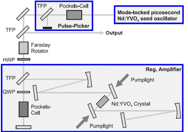
Fig.2.2.4: Schematic of the picosecond Nd:YVO4 oscillatoramplifier system
the Pockels cell allows the injecting the laser pulses selected by the pulse picker into the cavity of the amplifier. Finally, after several round trips, the amplified pulses with mJ level energy can be ejected from the resonator by the same optical elements.
Nowadays, commercial picosecond lasers based on this Nd:YVO4 oscillator amplifier system can generate 10ps laser pulses with maximum Ep ≈ 1mJ, e.g. High-Q IC-355-800ps, the picosecond laser system employed for current research (which will be discussed in more detail in Chapter 3). The output repetition rate of the pulses, up to several hundreds kHz, is tuneable by a function generator sending a signal to control the Pockels-cell. Moreover, the fundamental output wavelength of 1064nm can be frequency-doubled and tripled by properly adjusting the relevant half wave plate, generating 532nm and 355nm output, respectively [34].
2.2.2 Ultrashort pulse laser ablation of material
In micromachining with lasers, especially drilling and cutting, material removal takes place through the ablation process where the target material under laser irradiation absorbs energy and transforms into either a liquid or a vapour. The melted liquid is expelled from the interaction region by the recoil action, while the vapour removes itself directly from the focus. Additionally, other processes, e.g. heat conduction, radiation, and plasma expansion, are associated with the laser-material interaction.
material ablation and the difference with long pulse laser ablation are briefly introduced.
2.2.2.1 Absorption of laser energy
The first step in laser ablation is the absorption of laser energy by the target material. In the case of metals, laser energy is absorbed by free electrons due to inverse Bremsstrahlung. The absorption is followed by fast energy relaxation within the electronic subsystem, thermal diffusion, and energy transfer to the lattice due to electron–phonon coupling. Accordingly, the procedure of the energy transferring from laser pulses to the target material can be described by the following three stages [36-38] and is schematically shown in fig 2.2.5:
(i) light absorption
(ii)electron thermal diffusion (iii) electron-lattice relaxation.
Fig.2.2.5: Absorption of laser energy
( ) e e) ( )
e e e e l
T T
C T g T T Q
t x x
∂ ∂ ∂
= (κ − − +
∂ ∂ ∂ (2.2.5)
( ) l ( )
l l e l
T
C T g T T
t ∂
= −
∂ (2.2.6)
Te and Tl are the temperatures of electrons and the lattice, respectively, Ce and Cl are corresponding temperature dependent specific heat capacities, κe is the electron thermal conductivity, g is the electron-phonon coupling constant describing the energy exchange rate between electron and phonon subsystems, and Q is the laser power absorbed. Basically, the first equation 2.2.5 describes stages (i) and (ii), while the second equation 2.2.6 relates to stage (iii).
For most metallic materials, the time for electron-phonon coupling is from 1 to 100 picoseconds. For long laser pulses, e.g. nanosecond, where the pulse duration is much longer than lattice heating time, thermalization between the electron subsystem and the lattice takes place during the laser pulse. In this case the electrons and the lattice can be characterized by a common temperature T = Te = Tl. However, in the case of ultrashort pulse lasers, the ultra-short pulse duration (< 10ps), is comparable to or shorter than the time for energy electron-phonon coupling, and the ultra-high instantaneous intensity involved causes the electron temperature to be significantly higher than the lattice temperature during all the stages. Hence, the energy absorption takes place under the extreme non-equilibrium temperature difference between the electrons and the lattice.
2.2.2.2 Well defined ablation threshold with ultrashort pulses
from the long pulse induced threshold of material ablation, which has a large spread, the threshold at ultrashort pulse durations become more deterministic and precise [2].
Figure 2.2.6 shows a data for single-shot plasma emission generated by laser-induced ablation in fuse silica as a function of incident laser fluence for laser pulse duration of (a) 7ns and (b) 170fs [2]. As clearly shown in figure 2.2.6 (a), for long pulses the threshold has a large uncertainty. Some pulses with fluence considerately below the threshold value (the dash-line marked in the graph) caused plasma emission, indicating that material ablation was taking place, while some pulses with fluence far above the threshold did not cause ablation since no plasma emission was observed. However, the situation changes drastically when ultrashort laser pulses were used: the deviation in ablation threshold was well-defined in a very narrow range, as shown in figure 2.2.6 (b).
Fig.2.2.6: Single-shot plasma emission data of laser-induced breakdown in fused silica as function of incident laser fluence for laser pulse durations of (a) 7 ns and (b)
Due to the well-defined ablation threshold, the ablation of material can be precisely controlled by the input fluence of the ultrashort pulse laser, which shows one of the potential advantages for high precision micromachining.
2.2.2.3 ‘Thermal-free’ processing with ultrashort laser pulses
When the laser energy is deposited in a surface layer, the thickness of the layer is given by the optical penetration skin depth:
1
s
l α
= (2.2.7)
where α is the absorption coefficient. There is another characteristic length, which is the heat diffusion length during the laser pulse, giving the heat penetration depth due to thermal conduction. This diffusion length is given by:
d p
l = Dτ (2.2.8)
where D is the heat diffusion coefficient and τpis the laser pulse duration. For long
pulses, ld > ls, a great volume of the material can be heated by the laser pulse, hence
the temperature is determined by the heat diffusion length during the laser pulse. However, in the case of ultrashort pulses, as the laser pulse duration decreases to a value τp such thatld = Dτp <ls, the skin depth determines the heated volume during
the laser pulse, not the heat penetration depth. [39, 40]
waves. These shock waves can damage nearby device structures or delaminate multilayer materials. While the amplitude of the shock waves varies with the material being processed, it is generally true that the more energy is deposited in the micromachining process, the stronger the associated shock waves. Additionally, after ablation, the resolidification of the melt can lead to irregular shapes of the crater, and different mechanical properties from the original material.
Fig.2.2.7: Long pulse induced laser material ablation. [41]
On the other hand, as shown in figure 2.2.8, for ultrashort pulses, the deposited laser energy is limited in a layer with a thickness of ls. The localized energy heats the
and there is rapid cooling due to the steep temperature gradient. The heating of the material by heat diffusion is further reduced by the fact that a large amount of the absorbed laser energy is carried away by the direct vaporization. Because there is little liquid involved, ablation and material removal become highly precise, in contrast to the long pulse case.
Fig.2.2.8: Ultrashort pulse induced laser material ablation. [41]
absence of recast and beam deformation. This is due to nonlinear effects which can significantly degrade the machining quality in the case of metal ablation [42].
2.2.2.4 Material processing with picosecond laser pulses
From a laser-materials interaction point of view, Dausinger [42] argued that the mere reduction of pulse duration does not guarantee good machining quality and suggested that a pulse duration of 5 to 10 ps appears to be optimal for micromachining, especially for metals. A number of research groups have shown that picosecond laser micromachining can produce high machining quality combined with efficiency [43-47].
Fig.2.2.9 (a): Cross section profiles (left) and 3-D images (right) of single-pulse drilling of Au sample using a 10ps laser at a wavelength of 1064 nm under varied laser fluence under varied laser fluence: (a) F = 1 Jcm-2, (b) F = 5 Jcm-2, (c) F = 20 J
Fig.2.2.9 (b): Cross section profiles (left) and 3-D images (right) of single-pulse drilling of Au sample by using a 180 fs laser at a wavelength of 775 nm under varied
2.2.3 The limitations of ultrashort pulse laser processing
It has been demonstrated that there are two separate ablation regimes for ultrashort pulse laser ablation of material [48, 49]. For low laser fluences (F < 1 J/cm2), the ablation depth per pulse, L, can be described by the following expression [50, 51]:
1
ln( th l)
L≈ α− F F/ − (2.2.9)
where α-1 is the optical penetration skin depth and Fth-l is the ablation threshold for the
low fluence regime. At low laser fluence, the density of hot electrons is lower and the rate of electronic heat conduction is also lower. The electrons and lattice reach thermal equilibrium faster because of the smaller difference in electronic and lattice temperatures, thus allowing less time for electron thermal diffusion. Therefore the amount of energy transferring out of the optical skin depth is negligible and the ablation is characterized by the optical penetration skin depth.
At higher laser fluence (F > 1 J/cm2), the expression is changed to:
ln( )
d th h
L≈l F F/ − (2.2.10)
where ld is the electron heat diffusion length, and Fth-h is the ablation threshold for this
regime. In this case, due to the high incident laser fluence, the temperature reached by the electrons is higher and the rate of electronic heat conduction is greater. Therefore, thermal equilibrium between the electrons and lattice takes a longer time, hence allowing more time for electron thermal diffusion. Thus, the ablation is characterized by the electron heat diffusion length, ld, at higher fluences.
the strong plasma effects, shock waves and increased heat conduction losses, the ablation rate is saturated and thermal effects occur, strongly affecting the microprocessing efficiency and negating the advantages of ultrashort pulse laser processing [51-53].
The SEM pictures in figure 2.2.10 demonstrate the results of single pulse ablation of a polished aluminium sample with 150fs pulse length at low (a) and high (b) fluence [52]. Clearly, the result with low fluence, F ≈ 1.4J/cm2, shows negligible melt and fine scratches observed at the centre of the ablated region, while, at higher fluence, F ≈ 14 J/cm2, significant surface melting is observed in the crater with a recast ring around. The results confirm that significant thermal effects can still take place with ultrashort laser pulses and suggest that to minimize unwanted thermal effects, low pulse fluence is desirable.
Fig. 2.2.10: Single shot femtosecond ablation of polished aluminium, where F ≈ 1.4J/cm2 (a), F ≈ 14J/cm2 (b). [52]
thermal effects are minimized. Nevertheless, current ultrashort pulse laser systems (which are able to provide maximum output at the mJ level of pulse energy running at kilohertz repetition rate) have to severely attenuate their output making the processing significantly slow and inefficient. For instance, a Clarke-MXR 2010 system based on chirped pulse amplification, one of the ultrashort pulse laser systems used for the current research, can generate 180fs laser pulses (λ = 775nm) with maximum pulse energy Ep = 1mJ at 1kHz repetition rate. However, to ensure high quality, only less than 0.01mJ can be used for micro-machining with processing efficiency < 1%! This restriction may be one of the reasons why industrial uptake of kHz femtosecond systems has been limited.
2.3 Multiple beam parallel processing
Generating multiple beams, spatially splitting a mJ level energy laser pulse into many µJ laser pulses required for high quality non-thermal micro-machining, is a novel and
2.3.1 Parallel microfabrication of periodic structures
Periodic multiple beam patterns can be obtained by multi-beam interference of ultrashort laser pulses and used for parallel microfabrication [54-72]. Figure 2.3.1 schematically demonstrates an experimental design of material processing using this method [72]. A single beam was divided into several by a diffractive beam splitter (DBS). After a lens 1 (L1) and an aperture array (AA), five of the beams (α, β, γ, δ, ε) were selected to generate an interference pattern at the Fourier plane of a lens 2 (L2).
Fig. 2.3.2: Calculated intensity profiles of 2D periodic patterns. [72]
Due to interference, the intensity distribution ( )I r , was theoretically calculated as: 2
( ) i( )
i
I r =
∑
E r (2.3.1)Fig. 2.3.3: Scanning electron microscopy (SEM) images of the structure fabricated by the multi-beam interference of ultrashort pulses. (a) Top view, (b) oblique view of the
same sample, and (c) oblique view of another sample fabricated at larger exposure energy. [56]
Fig. 2.3.4: Basic scheme of optical setup. MLA: microlens array, L1: lens, DM: dichroic mirror, OL: objective lens. A is the plane where multiple foci are generated.
[75]
Figure 2.3.5 shows an optical micrograph of the fabricated structure on the surface of a glass substrate using a femtosecond laser system (τp ≈ 130fs) running at 1kHz repetition rate. Approximately 10×10 dots were fabricated in a square pattern by laser surface ablation. The total input pulse energy was approximately 120µJ with 5s irradiation period. The pitch of the fabricated dots was about 4.6µm.
2.3.2 Parallel microfabrication of arbitrary structures
Arbitrary multi-beam patterns can be generated by Diffractive Optical Elements (DOEs) which work as a hologram to modulate the input beam. With femtosecond laser pulses (τp ≈ 400fs, λ = 800nm), Y. Kuroiwa et al. successfully demonstrated both surface material ablation and internal structuring of a SiO2 glass sample using a DOE generated arbitrary multi-beam pattern [82], as shown in figure 2.3.6. The DOE, which had 4 phase levels and was designed with a wavelength of 800nm, was made of SiO2 glass with ¼ inch (6.35mm) thickness and an effective area of 8 mm × 8 mm.
Fig. 2.3.6: The results showing the microstructuring using a DOE generated arbitrary multi-beam pattern. (a) The designed focal shape of the pattern, (b)The modulated beam profile, (c) Surface view of ablation pattern observed by optical microscopy, (d) Processed are inside the glass observed by optical microscopy, left:
![Fig. 2.2.3: Diagramatic scheme of chirped pulse amplification [16]](https://thumb-us.123doks.com/thumbv2/123dok_us/8059053.225504/37.612.128.484.298.527/fig-diagramatic-scheme-chirped-pulse-amplification.webp)