This is a repository copy of
Multiscale modeling of spin transport across a diffuse interface
.
White Rose Research Online URL for this paper:
http://eprints.whiterose.ac.uk/119968/
Version: Accepted Version
Article:
Chureemart, J., Cuadrado, R., Chureemart, P. et al. (1 more author) (2017) Multiscale
modeling of spin transport across a diffuse interface. Journal of Magnetism and Magnetic
Materials. pp. 287-292. ISSN 0304-8853
https://doi.org/10.1016/j.jmmm.2017.07.085
[email protected] https://eprints.whiterose.ac.uk/ Reuse
This article is distributed under the terms of the Creative Commons Attribution-NonCommercial-NoDerivs (CC BY-NC-ND) licence. This licence only allows you to download this work and share it with others as long as you credit the authors, but you can’t change the article in any way or use it commercially. More
information and the full terms of the licence here: https://creativecommons.org/licenses/
Takedown
If you consider content in White Rose Research Online to be in breach of UK law, please notify us by
Multiscale modeling of spin transport across a diffuse interface
J. Chureemarta, R. Cuadradob,c,d, P. Chureemarta,∗, and R. W. Chantrellb
aComputational and Experimental Magnetism Group, Department of Physics, Mahasarakham University, Mahasarakham, 44150, Thailand
bDepartment of Physics, University of York, York, YO10 5DD, United Kingdom
cCatalan Institute of Nanoscience and Nanotechnology (ICN2), CSIC and BIST, Campus UAB, Bellaterra, 08193 Barcelona, Spain
dUniversitat Autonoma de Barcelona, 08193 Bellaterra (Cerdanyola del Valles), Spain
Abstract
We present multiscale calculations to describe the spin transport behavior of the Co/Cu bilayer stucture including the
effect of the interface. The multiscale approach introduces the connection between theab-initiocalculation used to
describe the electronic structure of the system and the generalized spin accumulation model employed to describe the spin transport behavior. We have applied our model to atomically smooth and diffuse interfaces. The results demonstrate the huge importance of the use of first principle calculations, not only due to the interfacial coordinates optimization but also the magnetic and electronic properties obtained through the electronic structure. The system including the effect of interface with and without the charge fluctuation are studied. The results indicate that changes of electronic structure at the Co/Cu interface give rise to an interfacial resistance distributed over several atomic planes, similar to the effect of interface diffusion. We argue that even atomically smooth Co/Cu interfaces have properties analogous to a diffuse interface due to the variation of electronic structure at the interface.
Keywords: spin transport, multiscale model, diffuse interface
1. Introduction
The understanding of spin transport and spin torque is of increasing importance for spintronic device ap-plications since the discovery of giant magnetoresis-tance (GMR) [1, 2] and tunnelling magnetoresismagnetoresis-tance (TMR). [3, 4] These phenomena have opened a new path for spintronic device design such as magnetic tunnelling junction (MTJ) sensors [5] and magneto-resistive random access memory (MRAM) [6] lead-ing to the development of new generations of com-puter architecture. In addition, read sensors for con-ventional magnetic recording rely on transport prop-erties to achieve the desired functionality. Both spin transport and spin torque are phenomena strongly af-fected by the interface structure and properties which will therefore play a crucial role in determining re-sistance arising from spin–dependent scattering at the interface.[7, 8, 9, 10, 11] From the theoretical point of view, the simulation of a general interface between two different materials is of great complexity. The usual
∗P. Chureemart, Email address: [email protected]
and easiest way to proceed is to have both alloys in
contact locating the atoms of one of the materials @
top,hollow,bridgeof the other. A more general situation would be when the atoms of both materials are allowed to move across to the interface leading to interdiffusion within the interfacial region. This diffusion leads in a different degrees of roughness depending on how much the alloys have mixed. Roughness at interfaces as well as the interfacial and intralayer scattering is of huge im-portance in relation to the objective of achieving high magnetoresistance (MR) [12, 11, 9].
theory is essentially a drift-diffusion model which only applies to incoherent systems much larger than the mean free path. However, it is important to note that macro-scopic models of the effects of a spin-polarized current are based [17] on the simple addition of spin-torque terms in the Landau-Lifshitz-Gilbert equation and, as shown by Claudio-Gonzalez et. al [18] and Chureemart et.al. [19], the phenomenological constants represent-ing the strength of the adiabatic and non-adiabatic terms are not spatially invariant; self-consistent solution of the spin accumulation and the magnetization is physically a better choice, and an advanced numerical implemen-tation for micromagnetics has been recently presented by Abert et.al. [20]. The proper treatment of interface effects was considered by Brataas et. al. [21] who in-troduced the concept of spin mixing conductance. Here we consider a further important effect of the nature of the interface, firstly related to the electronic properties and secondly to the presence of interfacial roughness; practically inevitable in sputtered devices.
The ZLF model has recently been generalized to al-low the investigation of diffuse interfaces. [22] The magnetic ion concentration at any given position of the system, determined via Fick’s law, gives rise to a spatial variation of the transport parameters within the inter-face. The model described in Ref. [22] is based on an approach which allows treatment of systems with spatially varying magnetization structures by calculat-ing the SA in a rotated coordinate system based on the direction of the local magnetization [19]. A feature of the model given in Ref. [19] is the calculation of the SA via the local spin polarizationm, equal to the local value of(n↑−n↓)where then↑(↓)represents the density of states (DOS) at the Fermi level, EF, as follows
dm
dt + (J/~)m×M=−
m−m∞
τs f
(1)
whereMis a unit vector along the local magnetization
direction,Jis the s−d exchange integral andτs f is the
spin–flip scattering time. Calculation ofmis convenient for the case of a current flowing between materials with differentm∞. [22] We note thatm∞= (n↑eq−n↓eq), where
theneq is the equilibrium bulk value which can be
ob-tained viaab initiocalculation. Further, the spin accu-mulation, denoted hereδm, is usually defined as the de-viation of the local spin polarization from equilibrium, i.e. δm= (n↑−n↓)−(n↑eq−n↓eq) = (m−m∞). We use
Eq. 1 because, although an additional dephasing term has been introduced by Petitjean et. al.[23], it has been shown that this can be absorbed into the damping term used in Eq. 1. The model derives stationary solutions
for mand subsequently the SAδmunder the
assump-tion that changes in the magnetizaassump-tion are much slower than the variation of the SA.
In this work, we focus on interface properties and their effect on the spin accumulation. First, we con-sider an atomically flat interface between two differ-ent materials. By means of Density Functional The-ory (DFT) calculations we investigate the interface elec-tronic structure and its effect on the spin accumulation. The interface is constructed as a periodicbccstructure (See Fig.1–A1 and B) without any roughness. This mul-tiscale approach will be applied to Co/Cu interface to investigate the spin transport behavior as well as evalu-ate the interfacial resistance. Secondly, we investigevalu-ate the properties of a diffuse interface created by mod-elling interdiffusion between the layers. Interestingly it is demonstrated that the interface resistance is spread over several atomic planes in both cases, showing that modification of the interface electronic structure has a similar effect to that of a diffuse interface. The paper is structured as follows. We first describe the spin
accu-mulation model including the calculation of m∞. We
then proceed to investigate the spin accumulation an atomically smooth interface, firstly under the simple as-sumption of an abrupt change of material properties at the interface. This contrasts strongly with the accumula-tion calculated for the realistic case taking into account
the spatial dependence of m∞ from the DFT
calcula-tions. Finally we present calculations of the spin accu-mulation for a diffuse interface, which shows a delocal-ization of the interface resistance similar to that arising from the spatial variation ofm∞.
2. Model description
2.1. Spin accumulation model
The full understanding of the mechanism behind GMR and TMR becomes important for the development of spin electronic technologies. The interface resistance can be calculated from the spin accumulation and sub-sequently gives rise to GMR. Consub-sequently, the calcu-lation of SA is required in order to gain insight into the spin transport behavior. Here, the SA is defined as the the difference of spin–up and spin–down electron
pop-ulations available from ab initio calculations. This is
essential to deal with multiple layers with different equi-librium value of SA. The general solution of spin accu-mulation is solved from Eq. (1) consisting of longitu-dinal (mk) and transverse components (m⊥,2andm⊥,3)
[22] following the equations
mk(x) = [mk(∞) + [mk(0)−mk(∞)]e−x/λsdl]bˆ 1
m⊥,2(x) = [G2e−x/l++G3e−x/l−]bˆ2
m⊥,3(x) = [−iG2e−x/l++iG3e−x/l−]bˆ3, (2)
in a rotated basis system whose axes ˆb1, ˆb2and ˆb3are
parallel ( ˆb1) and perpendicular ( ˆb2and ˆb3) to the local
magnetization. The coefficientsmk(0),G2andG3are
calculated by imposing continuity of the spin current at the interface [16] and 1/l∓=
q
(1/λ2
s f)±(i/λ2J). The
equilibrium valuemk(∞)is the difference between the spin–up and spin–down density of states (DOS) at the Fermi energy obtained fromab initiocalculations,
mk(∞) =[DOS↑(EF)−DOS↓(EF)]kBTe
V (3)
wherekBis the Boltzmann constant,T is the
tempera-ture,eis the electron charge andV is the unit cell vol-ume.
2.2. Ab-initio calculation of interface electronic prop-erties
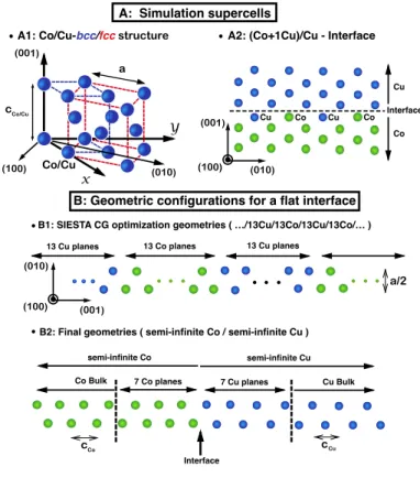
In principle, a model that describes the most gen-eral geometry of Co/Cu interface would be composed of a diffuse interface, i.e., a geometry where the atoms belonging to both alloys are “transferred” –after per-forming a molecular dynamics (MD) simulation, for example– from one alloy to the other, having semi– infinite materials on both sides composed of hundreds of atoms. Unfortunately, to model interfaces in this fash-ion is of extreme difficulty using pureab-initioMD cal-culations due to the huge number of atoms that would be involved. One possibility would be the use of clas-sical MD simulations but the information regarding the electronic structure would be lost. The reduction of the system size is then mandatory. In the present work, we study interface effects by the simulation of three differ-ent model systems. In case 1, the interface is taken as atomically smooth and the material properties change abruptly at the interface. In case 2 the interface is again taken as atomically smooth but the SA will be calculated using atomic layer resolved values ofm∞determined by
DFT calculations on systems with relaxed atomic posi-tions. The layers will be patterned by means of the con-tact of Co and Cu alloys with the same 2D periodicity and repeated periodically out–of–plane (001) as shown in figure 1–B2.
Finally, in case 3 we will create a simple model of a diffuse interface by the replacement of one Co atom within the interface plane by one Cu (see figure 1–A2).
Again, atomic layer-resolved values of m∞, calcuated
by DFT methods after relaxation, are used for the cal-culation of the SA. In this case, there is a computa-tional price to pay, in which we require large sizes of
13 Co planes 13 Cu planes 13 Cu planes
B: Geometric conÞgurations for a ßat interface
B1: SIESTA CG optimization geometries ( É/13Cu/13Co/13Cu/13Co/É )
B2: Final geometries ( semi-inÞnite Co / semi-inÞnite Cu ) (010)
(100) (001)
A1: Co/Cu-bcc/fccstructure
A: Simulation supercells
Co Cu
c c
a/2
A2: (Co+1Cu)/Cu - Interface
7 Cu planes 7 Co planes
Co Bulk
semi-inÞnite Co semi-inÞnite Cu
Interface
Cu Bulk (010)
(100) (001)
Cu
Cu Cu
Co Co Co Interface Co/Cu
x
Y
Co/Cu c
a
(010) (100)
(001)
Figure 1: (Color online) (A1) Schematic representation of the Co and Cu bcc/fcc bulk unit cells; (A2) Side view of the modeled diffusion interface employed in the present work; (B1) Periodic · · ·/13Co/13Cu/· · ·geometric configuration used in the conjugate gra-dient relaxation method; (B2) Final interface geometry between two semi–infinite Co and Cu bulk alloys after extract 7Co+7Cu slice from B1 relaxed coordinates.
the simulation supercells, having more atoms in the sim-ulation. However, we can minimize the computational tasks by choosing conveniently the unit cell. To this end, we observe that in our system the atomic stacking is along the (001) direction and if we inspect the fig-ure 1–A1, we can select eitherbccorfccto describe the physical systems since both unit cells depict the same structure. The choice of structure will be relevant be-cause of the number of atoms per supercell will be
dif-ferent. Consequently we choose thebccstructure due
po-tential we employed the generalized gradient
approxi-mation (GGA) [25]. We used double–ζpolarized (DZP)
strictly localized numerical atomic orbitals as basis set. We ensured the convergence of the magnetic moment as well as DOS used in the spin transport calculations by considering 196 k–points.
Fig.1–B describes schematically the construction process of the final· · ·Co/Cu· · ·geometry used in this work and its main geometric parameters. Each one of these materials have their own bulk lattice constants and to obtain them we optimized the geometry individ-ually. In doing so the Co and Cu lattice values were 3.54 and 3.68, respectively. We assume that Co and
Cu have the samebccstructure and that they share the
same in–plane lattice constanta, so we chose the mean value to be able to overcome the 4% mismatch between
them. On the other hand, in bulk phases a=c,
how-ever, when a changes the out–of–plane structure will
change and cCo,cCu. We performed conjugate
gra-dient relaxation (CG) to determine these out–of–plane parameters ensuring that the final forces between atoms were less than 0.05 eV/. As an initial guess we con-structed the configuration shown in 1–B1 for the peri-odic out–of–plane· · ·/13Co/13Cu/13Co/13Cu/· · ·
struc-ture. Due to the
Z
periodicity no vacuum is needed andeach Co/Cu interface experiences the same environment on both sides. This permits to avoid the use of any con-straint in the calculation and we were able to select at the end of the optimization 7Co+7Cu planes for the con-struction of the final geometry 1–B2. In between each two Co/Cu interfaces we ensured with high level of pre-cision that either Co or Cu plane exhibits bulk properties and hence we can join the slab on both sides to the semi– infinite parts. Finally, the resulting out–of–plane values were:cCo/a=0.96,cCu/a=1.06 and for the common in–
planea, 3.61. For the diffuse interface optimization, the same procedure was followed.
The diffusion of the magnetic ion concentration at any position for the · · ·Co/Cu· · · ferromagnetic/non– magnetic (FM–NM) structure is considered from the spatial variation of magnetic moment achieved from the
ab initiocalculations. The spatial concentration of mag-netic ion (Co) at any given positionxof the system can be modeled as the following equation,
CCo(x) =
NCo(x)µCo+NCu(x)µCu
[NCo(x) +NCu(x)]µCo
(4)
whereNCo,Cu(x)is the number of local ion of Co or Cu
at any positionxandµCo,Cu denotes the magnetic
mo-ment of Co or Cu. The calculated concentration from Eq. (4) is used to model the spatial variation of the dif-fusive transport parameters,P(x), taken as a linear
com-bination of the bulk parameters weighted by the local concentrations given by,
P(x) =PCoCCo(x) +PCu[1−CCo(x)] (5)
wherePCo,Cuis the diffusive transport parameters of Co
or Cu.
3. Results
To describe the physical mechanism of spin transport including the diffuse interface, we study the structure of the bilayer system of Co/Cu by employing the
mul-tiscale model, which calculates the SA withm∞
deter-mined from layer resolved ab initio information. We
consider the bilayer system of Co/Cu with three differ-ent interfaces as described earlier. Our general solution of SA is then applied to each system discretized into many thin layers to investigate the spin transport behav-ior and the interfacial resistance at any position in the system. In the following we consider each case in turn before giving an overall interpretation and drawing con-clusions.
3.1. Case 1: ideal interface with step change in prop-erties
We first consider the system with an ideal interface by assuming that the concentration of magnetic ion is constant throughout the Co layer. This case further as-sumes that the transport properties are spatially invari-ant in the Co and Cu layers. Specifically, we assume that the equilibrium value of SA,mk(∞), varies discon-tinuously from the bulk value of Co to that of Cu which is zero. The SA is then investigated by using our mod-ified solution in Ref. [22]. The system is discretized into many thin layers in order to calculate and observe the development of SA and spin current by applying the generalized formalism, which propagates the SA solu-tion layer by layer throughout the system.
As expected, the spin accumulation is not changed throughout Co layers with collinear magnetization as clearly shown in Fig. 2 (top). In addition, we focus on the spin transport behavior at the interface between layers. The SA is discontinuous at the interface corre-sponding to the discontinuity of the spin transport pa-rameters of Co and Cu layers at the interface. We note thatmin the Co layer decays very slowly in the Cu con-sistent with experiment, due to its large spin diffusion length [26]. The spatial resistance-area product (RA) can be calculated directly from the SA (δm) and spin current (jm) as follows,
RA=|∆δm|a 2k
BT tF
jme2
(6)
RA [f
Ω
·m
2 ]
Distance [x, nm]
0 0.04 0.08 0.12 0.16
-4 -3 -2 -1 0 1 2 3 4
δ
m [c/cm
3 ]
Co Cu
0 5 10 15 20
Figure 2: (Color online) (Top) Spatial spin accumulation and (Bot-tom) Interfacial resistance of the Co/Cu system with an ideal interface, i.e. atomically sharp with a step change of magnetic and transport pa-rameters.
where∆δmis the difference of SA across the layers,
kBT is 10meVor 1.6×10⁻²¹J,ais the lattice constant
of material,tF is the thickness between planes andeis
the electron charge. We calculatedRA between each
plane using Eq. (6) as shown in Fig. 2 (bottom). In the Co the corresponding resistance is zero due to the constant value of SA. Similarly in the Cu layer the slow variation of SA leads to essentially zero resistance. The interface resistance is confined to the boundary layer
due to the discontinuity in the SAwhich is consistent
with previous study by A. Fert et al. [27]. The total resistance-area product of the structure, a sum of bulk and interface resistances, can be obtained by summing the resistance along the direction of injected spin cur-rent. The interface resistance becomes dominant the re-sistance of the system. The total interface rere-sistance for
ideal Co/Cu interface is 0.16 fΩ·m2which gives
rea-sonable agreement with both the existing experimental
and theoretical values of 0.227 fΩ·m2[28, 29, 30].
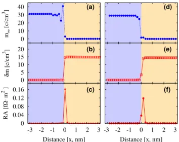
3.2. Case 2: atomically sharp interface withab initio
parameterization.
In this case, we study more realistic behavior of spin transport for an atomically structured interface of Co/Cu system by means of the multiscale approach which proceeds by relaxation of the interface and cal-culation of the DOS. Subsequently it leads to the calcu-lation of the equilibrium value of spin polarization from DOS↓(↑)(EF) [22]. The result in Fig. 3 (a) depicts the
RA [f
Ω
· m
2 ]
Distance [x, nm]
(c)
0 0.04 0.08 0.12 0.16
-3 -2 -1 0 1 2 3
δ
m [c/cm
3 ] (b)
0 5 10 15 20
m
∞
[c/cm
3 ]
(a)
0 10 20 30 40
Distance [x, nm]
(f)
-3 -2 -1 0 1 2 3
(e) (d)
Figure 3: (Color online) (a) (d) Spatial equilibrium value of spin ac-cumulation (b) (e) Spin acac-cumulation and (c) (f) Interfacial resistance of Co/Cu system for Case 2 (sharp interface with ab-initio parameter-ization) and Case 3 (rough interface) respectively
equilibrium valuemk(∞)from theab initiocalculations. Variations in the DOS close to the interface give rise firstly to a slight polarization of the Cu and secondly to oscillatory behavior in the Co layer close to the inter-face. The oscillations are due to the interfacial charge rearrangement between both Co and Cu species at the interface. The oscillations in the Co vanish for layers at distances greater than 1 nm, corresponding to the re-gion where the coordinates are similar to those in the Co bulk phase. Using theab initiovalues ofmk(∞)we next calculate the SA as a function of position illustrated in Fig. 3 (b). The SA closely follows the equilibrium value since the incoming spin current is fully polarized in the Co layer. Across the interface, the SA exhibits discon-tinuous behavior due to the different transport properties of the material of Co/Cu, gradually decreasing to zero associated with the spin diffusion length of Cu, (600 nm). Due to the oscillations in the electronic DOS in the Co, one also observes discontinuous behavior of the SA within the Co atomic layers close to the interface with the Cu.
distributed over several atomic planes around the inter-face. The phenomenon originates as a result of changes in the electronic structure of Co/Cu close to the bound-ary. In case 1 we made an implicit assumption that there are no charge fluctuations around the interface region. On the contrary, in the realistic case for Co/Cu interface it is also observable that, even though without species (atoms) transferred between alloys, the properties of a real interface are quite different from those predicted by the simplified model of case 1. The electronic structure modification after the geometry optimization, such as the hybridation between differents–dorbitals, indicates that our multiscale model, introducing interfacial effects through theab initio calculations within the atomistic model plays an important role in the prediction of the of the spin transport for any system involving interfaces such as studied here. The interface resistance for this
case is 0.172 fΩ·m2which is closer to the experimental
result [28, 29].
3.3. Case 3: Simple model of a diffuse interface
In practice, sharp interfaces are not expected in real spintronic devices since the sputtering process generally builds diffuse interfaces. As previously mentioned, it is of extreme complexity to perform DFT calculations of these real systems because of the simulation supercell size and hence the large amount of atoms involved. One step forward, compared to the previously studied cases 1 and 2, is the construction of a simple rough interface, where only one atom of one material is replaced by one of the other (see figure 1–A2). In doing so, we take the first step to understand more realistic diffuse inter-faces. As in case 2, the rough interface was optimized by means of CG method followed by the self-consistent calculation of the layer resolved DOS. Subsequently
mk(∞)is determined. In order to compare the present case with previous ones the layer resolvedmk(∞)values are shown in Fig. 3 (d). It reveals that the polarization extends further into the Cu due to an enhancement of the magnetic moment, and that the rough Co/Cu inter-face, considerably damps out the oscillations ofmk(∞)
present in the atomically sharp interface. The physical explanation of the reduction in the oscillatory behavior ofmk(∞)in the present case compared to cases 1 and 2 is lies in the smooth chemical transition between both materials which favors the gradual charge transfer be-tween Co and Cu at the mixed Co/Cu plane.
The transport parameters are estimated from the con-centration of magnetic ions. The values of the layer re-solved SA is given in Fig. 3(e). We observe that the SA exhibits discontinuous behavior close to the inter-face and shows damped oscillations compared to case
2. However, the spatial variation of the SA is again de-localized from the interface due to the combination of interface roughness and the spatial dependence on the electronic structure. This is reflected in the layer re-solved interface resistance RA as is shown in Fig 3 (f). Similar to case 2 we note that the interface resistance is delocalized from the interface region. For the rough Co/Cu interface, the total RA is approximately 0.175
fΩ·m2which is higher than that of ideal interface and
consistent with previous studies [28, 29].
4. Conclusions
In conclusion, we employed a recent developed for-malism of SA that allows to describe its behavior at any position of any FM–NM interface configuration. In ad-dition, the model makes the possibility for the treatment of systems with sharp variation of SA and also smoothly spatial magnetization concentrations. Furthermore, it is possible to use m∞ defined as the difference of the DOS↓and DOS↑at Fermi level, EF, quantities readily
available from theab initiocalculations. Hence, we pro-posed a multiscale model to give rise the possibility to study the spin transport behavior at any given position of any material through the quantum mechanical calcu-lations and atomistic simucalcu-lations.
We have applied the multiscale spin accumulation (MSA) model to the Co/Cu interface for 3 cases. Firstly, we considered the ideal case of an atomically smooth interface with a step change in properties at the inter-face. This system exhibits discontinuous behavior of the spin accumulation and an interface resistance local-ized to the Co/Cu boundary. We then investigated two more realistic cases, namely, case 2 assuming an atomi-cally smooth interface but with equilibrium polarization calculated fromab initiomodels and case 3 which intro-duced a first approximation to a rough interface. Both case 2 and case 3 give rise to similar delocalisation of the interface resistance, which is significant over a few lattice spacings. Interestingly, the rough interface gives rise to a smoother variation of the polarization close to the Co/Cu interface. Both case 2 and case 3 exhibit significantly increase values of interface resistance over and above the simplified model of case 1.
Clearly the presence of surface roughness; expected in practice due to the nature of the sputtering process by means of which most systems and devices are produced, has a significant effect on the transport properties as characterized here by the interface resistance. The result of a rough interface is to give rise to an increase of in-terface resistance which is delocalized from the Co/Cu
boundary and extends over a few lattice spacings. Inter-estingly, a similar effect is predicted for an atomically smooth interface which might be obtained by MBE. In this case the increased interface resistance and delocal-ization from the Co/Cu interface results from the mod-ification of the electronic properties of the Co and Cu due to the presence of the interface. The simple model of a bilayer as atomically smooth with a step change in properties is not sufficient, certainly to describe the properties of a Co/Cu bilayer. The properties are deter-mined by a complex mixture of the electronic density of states which gives rise to an oscillatory polarization in the Co and the interface roughness which, although it tends to damp out the DOS oscillations, still results in an increased interface resistance delocalised from the Co/Cu boundary.
Acknowledgements
PC and JC would like to acknowledge financial sup-port from Mahasarakham University (Thailand), the Newton Fund: researcher links travel grant 2015 and Thailand research fund Grant No. IAPP/151633. Finan-cial support of the Samsung SGMI program is gratefully acknowledged. This work made use of the facilities of N8 HPC provided and funded by the N8 consortium and EPSRC (Grant No. EP/K000225/1) co-ordinated by the Universities of Leeds and Manchester and the EP-SRC Small items of research equipment at the Univer-sity of York ENERGY (Grant No. EP/K031589/1). RC acknowledges the funding from the European Unions Horizon 2020 research and innovation programme un-der the Marie Sklodoswa–Curie grant agreement no. 665919 and also the support of ICN2 by the Severo Ochoa program from Spanish MINECO (Grant No. SEV-2013-0295) also the funding by the CERCA Pro-gramme/Generalitat de Catalunya.
References
[1] M. N. Baibich, J. M. Broto, A. Fert, F. N. Van Dau, F. Petroff, P. Etienne, G. Creuzet, A. Friederich, J. Chazelas, Giant mag-netoresistance of (001)fe/(001)cr magnetic superlattices, Phys. Rev. Lett. 61 (1988) 2472–2475.
[2] G. Binasch, P. Gr¨unberg, F. Saurenbach, W. Zinn, Enhanced magnetoresistance in layered magnetic structures with antifer-romagnetic interlayer exchange, Phys. Rev. B 39 (1989) 4828– 4830.
[3] S. S. P. Parkin, C. Kaiser, A. Panchula, P. M. Rice, B. Hughes, M. Samant, S.-H. Yang, Giant tunnelling magnetoresistance at room temperature with mgo (100) tunnel barriers, Nat Mater 3 (2004) 862–867.
[4] S. Yuasa, T. Nagahama, A. Fukushima, Y. Suzuki, K. Ando, Giant room-temperature magnetoresistance in single-crystal
fe/mgo/fe magnetic tunnel junctions, Nat Mater 3 (2004) 868– 871.
[5] D. W. Guo, F. A. Cardoso, R. Ferreira, E. Paz, S. Cardoso, P. P. Freitas, Mgo-based magnetic tunnel junction sensors array for non-destructive testing applications, Journal of Applied Physics 115 (17) (2014) –.
[6] K. Ando, S. Fujita, J. Ito, S. Yuasa, Y. Suzuki, Y. Nakatani, T. Miyazaki, H. Yoda, Spin-transfer torque magnetoresistive random-access memory technologies for normally off comput-ing (invited), Journal of Applied Physics 115 (17) (2014) –. [7] S. Zhang, P. M. Levy, Enhanced spin-dependent scattering at
interfaces, Phys. Rev. Lett. 77 (1996) 916–919.
[8] M. D. Stiles, D. R. Penn, Calculation of spin-dependent inter-face resistance, Phys. Rev. B 61 (2000) 3200–3202.
[9] L. Wang, W. J. McMahon, B. Liu, Y. H. Wu, C. T. Chong, In-terface or bulk scattering in the semiclassical theory for spin valves, Phys. Rev. B 69 (2004) 214403.
[10] T. M. Nakatani, T. Furubayashi, K. Hono, Interfacial resistance and spin-dependent scattering in the current-perpendicular-to-plane giant magnetoresistance using co2fe(al0.5si0.5) heusler alloy and ag, Journal of Applied Physics 109 (7).
[11] M. Ishikawa, H. Sugiyama, T. Inokuchi, K. Hamaya, Y. Saito, Effect of the interface resistance of cofe/mgo contacts on spin accumulation in silicon, Applied Physics Letters 100 (25) (2012) –.
[12] R. Q. Hood, L. M. Falicov, D. R. Penn, Effects of interfacial roughness on the magnetoresistance of magnetic metallic multi-layers, Phys. Rev. B 49 (1994) 368–377.
[13] J. Barna, G. Palasantzas, Interface roughness effects in the giant magnetoresistance in magnetic multilayers, Journal of Applied Physics 82 (8) (1997) 3950–3956.
[14] S. Agrawal, M. B. A. Jalil, S. G. Tan, K. L. Teo, T. Liew, Self-consistent ballistic and diffusive spin transport across interfa-cial resistances in a hybrid ferromagnet-semiconductor trilayer, Phys. Rev. B 72 (2005) 075352.
[15] N. L. Chung, M. B. A. Jalil, S. G. Tan, S. Bala Kumar, Interfa-cial resistance and spin flip effects on the magnetoresistance of a current perpendicular to plane spin valve, Journal of Applied Physics 103 (7) (2008) 070000.
[16] S. Zhang, P. M. Levy, A. Fert, Mechanisms of spin-polarized current-driven magnetization switching, Phys. Rev. Lett. 88 (2002) 236601.
[17] J. Thiaville, Y. Nakatani, J. Miltat, N. Suzuki, Europhys. Lett. 69 (1993) 990.
[18] D. Claudio-Gonzalez, A. Thiaville, J. Miltat, Phys. Rev. Lett. 108 (2012) 227208.
[19] P. Chureemart, I. D’Amico, R. W. Chantrell, Model of spin ac-cumulation and spin torque in spatially varying magnetisation structures: limitations of the micromagnetic approach, Journal of Physics: Condensed Matter 27 (14) (2015) 146004. [20] C. Abert, M. Ruggeri, F. Bruckner, C. Vogler, G. Hrkac, D.
Prae-torius, D. Suess, Europhys. Lett. 5 (2015) 14855.
[21] A. Brataas, G. Bauer, P. Kelly, Physics Reports 427 (2006) 157. [22] P. Chureemart, R. Cuadrado, I. D’Amico, R. W. Chantrell, Mod-eling spin injection across diffuse interfaces, Phys. Rev. B 87 (2013) 195310.
[23] C. Petitjean, D. Luc, X. Waintal, Unified drift-diffusion theory for transverse spin currents in spin valves, domain walls, and other textured magnets, Phys. Rev. Lett. 109 (2012) 117204. [24] J. M. Soler, E. Artacho, J. D. Gale, A. Garca, J. Junquera, P.
Or-dejn, D. Snchez-Portal, The siesta method for ab initio order-n materials simulatioorder-n, Jourorder-nal of Physics: Coorder-ndeorder-nsed Matter 14 (11) (2002) 2745.
3868.
[26] M. R. Sears, W. M. Saslow, Spin accumulation at ferromag-net/nonmagnetic material interfaces, Phys. Rev. B 85 (2012) 014404.
[27] A. Fert, H. Jaffr`es, Conditions for efficient spin injection from a ferromagnetic metal into a semiconductor, Phys. Rev. B 64 (2001) 184420.
[28] K. M. Schep, J. B. A. N. van Hoof, P. J. Kelly, G. E. W. Bauer, J. E. Inglesfield, Interface resistances of magnetic multilayers, Phys. Rev. B 56 (1997) 10805–10808.
[29] K. Xia, P. J. Kelly, G. E. W. Bauer, I. Turek, J. Kudrnovsk´y, V. Drchal, Interface resistance of disordered magnetic multilay-ers, Phys. Rev. B 63 (2001) 064407.
[30] J. Kimling, R. B. Wilson, K. Rott, J. Kimling, G. Reiss, D. G. Cahill, Spin-dependent thermal transport perpendicular to the planes of co/cu multilayers, Phys. Rev. B 91 (2015) 144405.