Quantum photonics hybrid integration platform
E. Murray, D. J. P. Ellis, T. Meany, F. F. Floether, J. P. Lee, J. P. Griffiths, G. A. C. Jones, I. Farrer, D. A. Ritchie
, A. J. Bennett, and A. J. Shields
Citation: Applied Physics Letters 107, 171108 (2015); doi: 10.1063/1.4935029
View online: http://dx.doi.org/10.1063/1.4935029
View Table of Contents: http://scitation.aip.org/content/aip/journal/apl/107/17?ver=pdfcov
Published by the AIP Publishing
Articles you may be interested in
On-chip beamsplitter operation on single photons from quasi-resonantly excited quantum dots embedded in GaAs rib waveguides
Appl. Phys. Lett. 107, 021101 (2015); 10.1063/1.4926729
On-chip electrically controlled routing of photons from a single quantum dot Appl. Phys. Lett. 106, 221101 (2015); 10.1063/1.4922041
Monolithic integration of a quantum emitter with a compact on-chip beam-splitter Appl. Phys. Lett. 104, 231107 (2014); 10.1063/1.4883374
On-chip single photon emission from an integrated semiconductor quantum dot into a photonic crystal waveguide Appl. Phys. Lett. 99, 261108 (2011); 10.1063/1.3672214
Quantum photonics hybrid integration platform
E.Murray,1,2D. J. P.Ellis,1T.Meany,1F. F.Floether,1,2J. P.Lee,1,3J. P.Griffiths,2
G. A. C.Jones,2I.Farrer,2D. A.Ritchie,2A. J.Bennett,1,a)and A. J.Shields1 1
Cambridge Research Laboratory, Toshiba Research Europe Limited, 208 Science Park, Milton Road, Cambridge CB4 0GZ, United Kingdom
2
Cavendish Laboratory, University of Cambridge, J.J. Thomson Avenue, Cambridge CB3 0HE, United Kingdom
3
Engineering Department, University of Cambridge, 9 J. J. Thomson Avenue, Cambridge CB3 0FA, United Kingdom
(Received 1 July 2015; accepted 21 October 2015; published online 29 October 2015)
Fundamental to integrated photonic quantum computing is an on-chip method for routing and modulating quantum light emission. We demonstrate a hybrid integration platform consisting of arbitrarily designed waveguide circuits and single-photon sources. InAs quantum dots (QD) embedded in GaAs are bonded to a SiON waveguide chip such that the QD emission is coupled to the waveguide mode. The waveguides are SiON core embedded in a SiO2 cladding. A tuneable
Mach Zehnder interferometer (MZI) modulates the emission between two output ports and can act as a path-encoded qubit preparation device. The single-photon nature of the emission was verified using the on-chip MZI as a beamsplitter in a Hanbury Brown and Twiss measurement.VC 2015
AIP Publishing LLC. [http://dx.doi.org/10.1063/1.4935029]
Linear optical quantum computing has been proven to be computationally efficient with single-photon-sources, beams-plitters, and phase shifters.1Although few photon gates have been demonstrated using bulk optics,2scaling to more com-plex circuits requires an integrated photonic technology.3
Integrated photonics offers the potential for true scal-ability due to component miniaturisation. Stscal-ability is intrin-sic to the platform and offers a reduction in complexity and size of the device.4Many of the elements needed for linear optical quantum computing can be manufactured on-chip. High-fidelity beam splitters and Mach Zehnder interferome-ters (MZIs) can be made with various semiconductor platforms5–7 as well as on-chip detectors.8,9 However, thus far, integration of single-photon sources into low-loss waveguides remains an open issue.
Semiconductor III-V quantum dots (QDs) have been shown to produce bright, single-photon emission,10 emit indistinguishable and entangled photons,11,12 can be site-controlled,13 and compatible with semiconductor foundry techniques. Various approaches for embedding QDs into integrated circuits are being explored. Photonic crystal waveguides yield high coupling efficiency of the QD emis-sion into the in-plane propagating waveguide mode.14,15 They can produce in-plane indistinguishable photons.16 However, as of yet in photonic crystal waveguides, no directional couplers or active modulators with embedded QDs have been demonstrated. QDs embedded in ridge waveguides in GaAs have been reported combined with the on-chip superconducting single-photon detectors.17 Air-clad GaAs ridge waveguides have also demonstrated QD integrated directional couplers.18,19 Other approaches use heralded single-photons from spontaneous parametric
down conversion integrated with waveguide chips.20
However, this approach lacks deterministic emission.
In this letter, we present a platform for hybrid integra-tion of III-V QDs with silicon oxynitride waveguides. A GaAs chip containing InAs quantum dots is bonded orthogo-nally to the SiON chip such that the photons emitted from the surface of the GaAs chip are routed into a guided mode. The quantum dots are embedded in a distributed Bragg reflector cavity with alternating layers of AlAs and GaAs. The SiON chip includes waveguide to deliver laser excita-tion light to the quantum dots and a return line consisting of a MZI. The MZI can act as a qubit preparation device for the single-photons emitted from the QD. If a single-photon impinges on the MZI, it will be placed into a path-encoded superposition of each output mode. The probability ampli-tude of being in each mode is chosen by the tuning of the MZI. This SiON technology is compatible with the creation of arbitrary designs of beamsplitters, MZIs, and phase shifters.
Orthogonal bonding allows the surface emission from the QD to be optimised by growing a distributed Bragg reflector cavity and/or creating a micropillar structure. Previous reports show efficiencies of out-of-plane QD col-lection as high as 0.75 into free space high numerical aper-ture objectives.21,22In the device presented here, the SiON waveguide numerical aperture is 0.3. The hybrid platform also has the potential for diode structures to be created for electrically driven or tuneable QD devices integrated with the waveguides.
Figure 1(a) shows a photograph of a hybrid device. A strip of III-V containing QDs is bonded to one end of the SiON waveguide chip. The QD source was grown by molec-ular beam epitaxy. A QD density was chosen such that a dot, which emits in the centre cavity mode, is aligned with a waveguide. The central cavity wavelength is 910 nm. Plasma enhanced chemical vapour deposition was used to create a layer of SiO2undercladding and SiON core on a silicon
sub-strate. Electron-beam lithography and reactive ion etching
a)
Electronic mail: [email protected]
were used to define the SiON core profile before finally a SiO2overclad layer was deposited. The orthogonal bonding
method allows the surface emission from the QD to be col-lected by the waveguide. The photons are routed into the waveguides, two sequential directional couplers form a MZI with a nickel-chromium alloy heater, applying a local phase shift to one MZI arm. A polarisation-maintaining V-groove array is aligned and attached to the waveguides for collec-tion. The device is kept at 4 K for the duration of the experiments.
Figure 1(b)shows the optical schematic of the experi-ments. A single channel delivers laser light. The QD light is returned through the MZI and collected into fibre by the V-groove array. The V-groove fibres are sent directly to a spectrometer. For time resolved experiments, transmission gratings are used to spectrally filter the emission before send-ing the light to avalanche photodiodes.
The characteristics of the device were simulated by using the finite difference time domain package MEEP.23,24 A^z oriented dipole emitter was placed in the centre of the cavity spacer aligned to the centre of the waveguide. A perfectly matched layer was placed at the edges of the simu-lation domain to absorb all light and prevent unwanted reflections. The^zcomponent of the electric field is shown in
Fig.1(c). There is a clear emission pattern along the wave-guide core.
The efficiency of this device was determined theoreti-cally. A bounding box, which records the Fourier trans-formed fields, was placed at the edge of the domain and just inside the perfectly matched layer. From this bounding box, the total power spectrum is recorded when the system is excited with a short Gaussian pulse. Another flux plane is placed across the waveguide. The waveguide core size was 1.6lm and the far field propogating mode has a spatial 1=e
width of 1.88lm which was chosen as the size of the wave-guide flux plane. It is placed sufficiently far from the surface of the III-V structure so that only the waveguide propagating mode is measured. Taking the ratio of the light propagating in the waveguide to the total in the bounding box gives the efficiency of the QD emission into the waveguide to be 2.8%. This is considerably higher for a QD in bulk of 0.5% and could be further enhanced with higher-Q cavities.
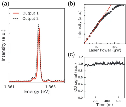
The integrated device is fixed, once the bonding is com-plete. This creates stability and no drifting in emission inten-sity is seen over the course of 12 h. The QD inteninten-sity as a function of time is plotted in Fig.2(c). The MZI was tuned to 50:50 and the spectrum from both outputs of the device can be seen in Fig.2(a). The QD analysed was located at the centre of the cavity mode at 1.362 eV. A power dependent spectrum was recorded as seen in Fig. 2(b). The emission, before saturation, is approximately linear (P0.95) implying an exciton and not a higher order complex.25The peak does not exhibit the polarisation splitting which is characteristic of a neutral exciton26,27 and is therefore likely to derive from a charged exciton.
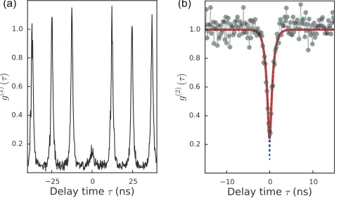
To verify the single-photon nature of the QD emission, a Hanbury Brown and Twiss experiment was recorded using the on-chip MZI as a beamsplitter. Using MZI’s on chip is a powerful technique due to the reconfigurability of the circuit.3They can be used as directional couplers with cho-sen reflectivity. The emission from both MZI output arms (ports 1 and 2 in Fig. 1(b)) was sent through two different
FIG. 1. (a) Photograph of a bonded device. (b) Schematic of the prototype device. The orange line indicates the waveguide to deliver excitation light; the red line indicates the waveguides travelled by the QD emission. (c) Finite-difference time domain simulation of a QD dipole emitting in a cavity and the emission being guided by the SiON core.
FIG. 2. (a) Spectrum from both output ports of the device indicated in red and black. (b) Power dependence of the spectral line at 1.362 eV. (c) Power output from the QD line over the course of 12 h.
[image:3.612.59.294.54.414.2] [image:3.612.315.559.528.734.2]transmission gratings for spectral filtering and then sent to avalanche photodiodes. The clicks on each detector were correlated. The value ofgð2ÞðsÞwas determined by normalis-ing the correlation histogram to havegð2ÞðsÞat the maximum
delay to unity, when the photons are uncorrelated. The
gð2ÞðsÞ function is given by gð2ÞðsÞ ¼ hIðtÞihIðtþsÞi= hIðtÞIðtþsÞÞi. An absence of correlation coincidences at time s¼0 implies that the device is a good single-photon source. The second order correlation curves were taken
under continuous wave (CW) (k¼810 nm) and pulsed
(k¼850 nm) excitation. The curves are shown in Fig.3. In the case of the pulsed curve (shown in Fig.3(a)), the signal to noise ratio due to dark counts of the detectors was calcu-lated and subtracted. A time window was also applied to the data, since the lifetime of the QD was 67063 ps. The vast majority (96%) of QD emission resides in a 4 ns window. So only coincidences inside this window were used for calculat-ing thegð2Þð0Þvalue of 0.19. The laser was delivering 3 ps
long pulses, but the carriers created in the GaAs bandgap may live for 100 s of ps before decay, so the dot can refill over a 100 ps timescale. After emission, the QD will remain empty until the next pulse. The QD emission is then a regu-lated stream of photons synchronised to the clock of the laser.
In the CW case, as seen in Fig.3(b), the black circles cor-respond to the data. The red line is a fit to the data. The dashed blue line is a fit, which takes into account the Gaussian response function of the detectors and timing system, and thus is a representation of the truegð2Þð0Þof the source. Thegð2Þð0Þ
value was taken from this fit to be 0.09. In CW excitation, the QD can emit a photon and immediately be repopulated due to the constant excitation of carriers around the QD. The stream of photons is still made up of antibunched photons; however, there is no time synchronisation.
Although it is well known that a MZI can be thought of a generalised tuneable beamsplitter,3,28 the statistics of the photon source were pre-characterised in those cases. If the source is known to be emitting single photons, the MZI gives the same correlation as a single beamsplitter. Fig.3(b)shows
gð2Þð0Þto be 0.09, after the system response is accounted for, indicating the sub-Poissonian statistics of the source.
The active modulation of the MZI was tested on the single-photon source. A voltage was applied to the heater on
one arm of the MZI. This induces local heating of the arm and a change in the refractive index of the waveguide core. This change creates a relative phase between the light in each arm of the MZI. At the second directional coupler, the light will constructively or destructively interfere, depending on the relative phase, and couple between the two output ports. Thus, emission coupling to each output arm of the MZI then varies as a function of the applied voltage. The coupling ratio of the device is defined as the power in one arm divided by the sum: r¼P1=ðP1þP2Þ, wherePi is the power in output port i in Fig. 1(b). The coupling ratio is shown in Fig.4along with the calculated phase.29The black line is a fit to the coupling ratio, extrapolated after 22 V to show the expected behaviour. It is seen that the phase (red line) is zero when all the light is coupled to port 1. Apphase shift is seen when the voltage is changed from 0 V to 22 V.
In conclusion, we have demonstrated a method for inte-grating a III-V quantum light source with a SiON waveguide platform. The single-photon nature of the source was verified using on-chip components, and the active modulation of the emission was demonstrated. This device shows potential for the integration of site controlled13,30 QDs granting precise alignment of multiple QDs with multiple waveguides allow-ing for scalable quantum manipulation.
E.M. and T.M. acknowledge support by the Marie Curie Actions within the Seventh Framework Programme for Research of the European Commission, under the Initial Training Network PICQUE (Grant No. 608062). F.F. acknowledges support from both the EPSRC and Toshiba Research Europe Ltd., Cambridge. J.L. acknowledges support from both the EPSRC CDT in Photonic Systems Development and Toshiba Research Europe Ltd., Cambridge. The authors acknowledge funding from the EPSRC for the MBE system used in the production of the QD samples.
1
E. Knill, R. Laflamme, and G. J. Milburn,Nature409, 46–52 (2001). 2
J. L. O’Brien, G. J. Pryde, A. G. White, T. C. Ralph, and D. Branning, Nature426, 264–267 (2003).
3
J. Carolan, C. Harrold, C. Sparrow, E. Martn-Lpez, N. J. Russell, J. W. Silverstone, P. J. Shadbolt, N. Matsuda, M. Oguma, M. Itoh, G. D. Marshall, M. G. Thompson, J. C. F. Matthews, T. Hashimoto, J. L. OBrien, and A. Laing,Science349, 711–716 (2015).
[image:4.612.328.547.51.214.2]FIG. 3. (a) Second order correlation function under pulsed excitation. (b) Second order correlation function under continuous wave excitation. The black circles are the raw data, the red line is a fit to the data, and the dashed blue line is the fit taking the Gaussian system response into account.
[image:4.612.56.297.583.724.2]4A. Politi, J. C. Matthews, M. G. Thompson, and J. L. O’Brien,IEEE J.
Sel. Top. Quantum Electron.15, 1673–1684 (2009). 5
J. Wang, A. Santamato, P. Jiang, D. Bonneau, E. Engin, J. W. Silverstone, M. Lermer, J. Beetz, M. Kamp, S. H€oflinget al.,Opt. Commun. 327, 49–55 (2014).
6
Y. Zhang, L. McKnight, E. Engin, I. M. Watson, M. J. Cryan, E. Gu, M. G. Thompson, S. Calvez, J. L. O’Brien, and M. D. Dawson,Appl. Phys. Lett.99, 161119 (2011).
7
A. Politi, M. J. Cryan, J. G. Rarity, S. Yu, and J. L. O’Brien,Science320, 646–649 (2008).
8
T. Gerrits, N. Thomas-Peter, J. C. Gates, A. E. Lita, B. J. Metcalf, B. Calkins, N. A. Tomlin, A. E. Fox, A. L. Linares, J. B. Springet al.,Phys. Rev. A84, 060301 (2011).
9
R. H. Hadfield,Nat. Photonics3, 696–705 (2009). 10
A. J. Bennett, D. C. Unitt, P. Atkinson, D. A. Ritchie, and A. J. Shields, Opt. Express13, 50–55 (2005).
11Y.-M. He, Y. He, Y.-J. Wei, D. Wu, M. Atat€ure, C. Schneider, S.
H€ofling, M. Kamp, C.-Y. Lu, and J.-W. Pan, Nat. Nanotechnol. 8, 213–217 (2013).
12R. Stevenson, C. Salter, J. Nilsson, A. Bennett, M. Ward, I. Farrer, D. Ritchie, and A. Shields,Phys. Rev. Lett.108, 040503 (2012).
13
G. Juska, V. Dimastrodonato, L. O. Mereni, A. Gocalinska, and E. Pelucchi,Nat. Photonics7, 527–531 (2013).
14A. Schwagmann, S. Kalliakos, I. Farrer, J. P. Griffiths, G. A. Jones, D. A. Ritchie, and A. J. Shields,Appl. Phys. Lett.99, 261108 (2011).
15
M. Arcari, I. S€ollner, A. Javadi, S. L. Hansen, S. Mahmoodian, J. Liu, H. Thyrrestrup, E. H. Lee, J. D. Song, S. Stobbeet al.,Phys. Rev. Lett.113, 093603 (2014).
16S. Kalliakos, Y. Brody, A. Schwagmann, A. J. Bennett, M. B. Ward, D. J.
Ellis, J. Skiba-Szymanska, I. Farrer, J. P. Griffiths, G. A. Jones et al., Appl. Phys. Lett.104, 221109 (2014).
17G. Reithmaier, S. Lichtmannecker, T. Reichert, P. Hasch, K. M€uller, M.
Bichler, R. Gross, and J. J. Finley,Sci. Rep.3, 1901 (2013). 18
N. Prtljaga, R. Coles, J. O’Hara, B. Royall, E. Clarke, A. Fox, and M. Skolnick,Appl. Phys. Lett.104, 231107 (2014).
19K. D. J€ons, U. Rengstl, M. Oster, F. Hargart, M. Heldmaier, S. Bounouar,
S. M. Ulrich, M. Jetter, and P. Michler, J. Phys. D: Appl. Phys.48(8), 085101 (2015).
20T. Meany, L. A. Ngah, M. J. Collins, A. S. Clark, R. J. Williams, B. J.
Eggleton, M. Steel, M. J. Withford, O. Alibart, and S. Tanzilli, Laser Photonics Rev.8, L42–L46 (2014).
21
J. Claudon, J. Bleuse, N. S. Malik, M. Bazin, P. Jaffrennou, N. Gregersen, C. Sauvan, P. Lalanne, and J.-M. Gerard,Nat. Photonics4, 174–177 (2010). 22M. Munsch, N. S. Malik, E. Dupuy, A. Delga, J. Bleuse, J.-M. Gerard, J.
Claudon, N. Gregersen, and J. Mørk,Phys. Rev. Lett.110, 177402 (2013). 23
A. F. Oskooi, D. Roundy, M. Ibanescu, P. Bermel, J. D. Joannopoulos, and S. G. Johnson,Comput. Phys. Commun.181, 687–702 (2010).
24V. A. Mandelshtam and H. S. Taylor,J. Chem. Phys.
107, 6756–6769 (1997). 25
M. Grundmann and D. Bimberg,Phys. Rev. B55, 9740 (1997). 26
M. Bayer, G. Ortner, O. Stern, A. Kuther, A. Gorbunov, A. Forchel, P. Hawrylak, S. Fafard, K. Hinzer, T. Reinecke et al., Phys. Rev. B65, 195315 (2002).
27
D. Gammon, E. Snow, B. Shanabrook, D. Katzer, and D. Park,Phys. Rev. Lett.76, 3005 (1996).
28N. C. Harris, G. R. Steinbrecher, J. Mower, Y. Lahini, M. Prabhu, T. Baehr-Jones, M. Hochberg, S. Lloyd, and D. Englund, preprint arXiv:1507.03406.
29
J. C. Matthews, A. Politi, A. Stefanov, and J. L. O’Brien,Nat. Photonics3, 346–350 (2009).
30A. Jamil, J. Skiba-Szymanska, S. Kalliakos, A. Schwagmann, M. B. Ward,
Y. Brody, D. J. Ellis, I. Farrer, J. P. Griffiths, G. A. Joneset al.,Appl. Phys. Lett.104, 101108 (2014).