Efficient Inner Receiver Design for OFDM-Based
WLAN Systems: Algorithm and Architecture
Alfonso Troya,
Member, IEEE,
Koushik Maharatna,
Member, IEEE,
Milo˘s Krsti´c, Eckhard Grass,
Ulrich Jagdhold, and Rolf Kraemer,
Member, IEEE
Abstract— In this article we propose a complete solution for the so-called Inner Receiver of an OFDM-WLAN system based on the IEEE 802.11a standard. We concentrate our investigations on three key components forming the Inner Receiver namely, the Synchronizer, the Channel Estimator and the Digital Timing Loop. The main goal is the joint optimization of the signal processing algorithms along with the implementation friendly VLSI architecture required for these three key components in order to reduce power, area and latency, without compromising the performance excessively. We provide both the mathematical details and extensive computer simulations to validate our design.
Index Terms— Channel estimation, OFDM, synchronization,
wireless LAN.
I. INTRODUCTION
T
HE use of the OFDM (Orthogonal Frequency Division Multiplex) transmission technique has gained a lot of interest in the recent years due to its spectral efficiency and capability to overcome multi-path fading. In this paper we concentrate on the OFDM-WLAN (Wireless Local Area Network) systems, which are already a reality thanks to the IEEE 802.11a/g standards [1], [2]. The application of OFDM is not restricted to these two standards, but new standardization processes already foresee the application of OFDM in future WLAN [3] and UWB (Ultra Wideband) systems [4].The key property of OFDM is orthogonality. By this prop-erty the system uses the input data to modulate a number of mutually orthogonal sub-carriers. This technique facilitates a high data rate transmission system. However, the whole system performance depends on maintaining the orthogonality of the sub-carriers. If the orthogonality property gets disturbed, unwanted effects such as Inter-Carrier Interference (ICI) and Inter-Symbol Interference (ISI) will occur during signal recep-tion. In general, the orthogonality property of the sub-carriers can be disturbed during the RF Up- and Down-conversion. On top of that the characteristic of the transmission channel may also affect the orthogonality condition. A number of authors
Manuscript received July 5, 2005; revised January 11, 2006 and May 29, 2006; accepted July 17, 2006. The associate editor coordinating the review of this paper and approving it for publication was C. Xiao.
A. Troya was with IHP, Frankfurt (Oder), Germany. He is now with Infineon Technologies AG, COM PS CE ALG, 81726 Munich, Germany (e-mail: [email protected]).
K. Maharatna is with the University of Southampton, University Road, Southampton, SO17 1BJ, UK (e-mail: [email protected]).
M. Krsti´c, E. Grass, U. Jagdhold, and R. Kraemer are with IHP, Frankfurt (Oder), Germany (e-mail: {krstic, grass, jagdhold, kraemer}@ihp-microelectronics.com).
[image:1.567.300.528.184.262.2]Digital Object Identifier 10.1109/TWC.2007.05481.
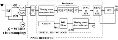
Fig. 1. General block diagram of the proposed Inner Receiver.
have addressed the impact of this type of impairments on OFDM signals in the past years [5], [6]. Thus, in order to make the system work efficiently, we need to re-establish the orthog-onality condition at the receiver. The so-calledInner Receiver (this term was firstly coined by Heinrich Meyr [7]) is used for this purpose. In essence, there are two main operations carried out inside the Inner Receiver (IRx) namelySignal Acquisition and Channel Correctionas shown in Fig. 1. The acquisition operation is performed by means of a synchronization block, which should be able to perform reliable Frame Detection (FD), and to provide estimations for the Carrier Frequency Offset (CFO) and Symbol Timing Offset (STO). The channel correction operation is needed to estimate and compensate the Channel Transfer Function (CTF), provided that orthogonality has been restored to a great extent by the synchronizer. The final goal is to supply the decoding and demodulator block with In-phase and Quadrature components that are as similar as possible to the original ones.
Though the IRx is an integrated part of the OFDM-based WLAN system, its design complexity is frequently underestimated. Unfortunately the standards do not provide in general any hints on how to implement the IRx, but it is left as a developer’s task. In this article we investigate an efficient realization of the IRx for IEEE 802.11a systems both from the algorithm and VLSI (Very Large Scale Integration) implementation point of view, and provide a complete and practical solution for it. The results developed in this work are applicable to the future standards [3]. In order to develop our solution we start with the algorithm level formulation of the desired functionality of the IRx. The algorithmic development has been considered strictly in conjunction with the possible architectural feasibility of an ASIC (Application Specific Integrated Circuit) implementation. Thus ajoint algorithm and architecture optimization has been undertaken using power consumption, silicon area, system latency and overall noise performance as the “quality/efficiency” parameters for the system. The power consumption and silicon area have been
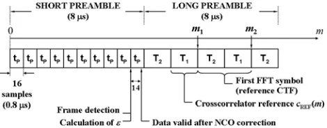
Fig. 2. Preamble symbols as defined by the 802.11a standard together with the timing schedule followed inside the Synchronizer.
considered as two of the main parameters since the system is targeted for mobile and portable applications where saving of battery life as well as the total size of the system are crucial. Latency has been considered from the operation principle of the IEEE 802.11a MAC (Medium Access Control) protocol [1].
Different parts of the present work have been published in different renowned conferences in short form [8], [10], [11], [19]. In this paper we provide a much more detailed and integrated view of the complete IRx solution. The rest of the present paper is organized as follows: after introduction, the main components of the IRx are investigated. Subsequently, an efficient synchronizer architecture is examined in Section II, whose main architecture was foreseen by the authors in [8], [9]. Section III is devoted to the analysis of a decision-directed Channel Estimator (CE). Two blocks are the main focus of our investigations, namely the Noise Reduction Filter (NRF) and the Residual Phase Error (RPE) correction block. The proposed timing loop is analyzed in detail in Section IV and provides a simple method to compensate for the Sampling Clock Frequency Offset (SCFO) based on the RPE estimation supplied by the CE. Section V presents simulation results which show the performance features of the proposed solu-tions. Finally, in Section VI, some important conclusions are derived.
II. THESYNCHRONIZER
The synchronizer is the block responsible for signal acquisi-tion. This term encompasses a number of operations that need to be performed in a very limited period of time in order to minimize latency. For our purpose, synchronization must be finished within the preamble time, i.e. 16μs, and the following operations must be performed based on the preamble symbols:
1) Frame detection.
2) Determination of the symbol timing.
3) Carrier frequency offset estimation and correction. 4) Extraction of the reference channel estimation.
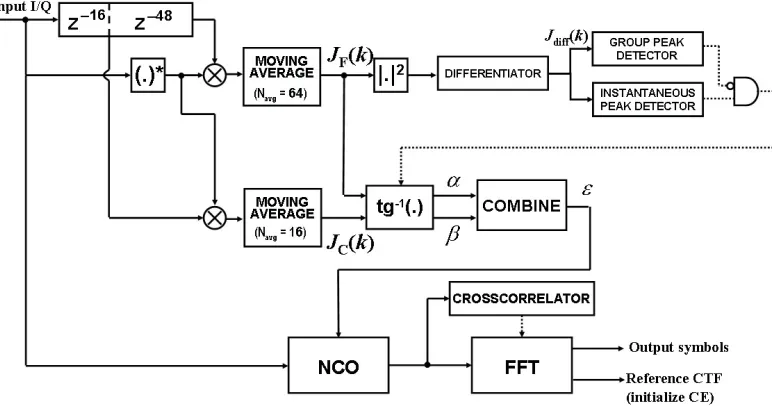
The order in which these operations are carried out strongly determines the architecture of the synchronizer. The preamble symbols in the 802.11a standard comprise a number of peri-odic sequences as shown in Fig. 2. This periperi-odic structure suggests a solution based on autocorrelators [13], [14]. The proposed implementation shown in Fig. 3 contains two autocorrelators. Each one encompasses a delay line (FIFO-type buffer) of length Nd, a complex conjugate operation, a
complex multiplier, and a moving average of length Navg. The moving average is an FIR filter of length Navg with all its coefficients being 1. Let’s consider the input signalr(m) to be sampled at frequencyfsand affected by a CFOf = Δf, where stands for the normalized CFO, andΔf is the sub-carrier spacing in the OFDM signal (Δf = 312.5 KHz in the 802.11a). Hence, the input signalr(m) can be expressed as
r(m) =s(m)·ej2πΔfsfm+v(m), (1)
where j = √−1, s(m) is the original time sequence and v(m) represents a zero-mean white Gaussian noise process. According to (1), the autocorrelator’s output signal Jx(k) is given by
Jx(k) = Navg−1
l=0
r∗(l−k)·r(l−k−Nd)
= e−j2πΔffsNd·
Navg−1
l=0
s∗(l−k)·s(l−k−Nd)
+
Navg−1
l=0
s∗(l−k)·v(l−k−Nd)·e− j2πΔff
s·(l−k)
+
Navg−1
l=0
v∗(l−k)·s(l−k−Nd)·e j2πΔff
s·(l−k−Nd)
+
Navg−1
l=0
v∗(l−k)·v(l−k−Nd), (2)
where the suffic xrepresents either F or C in Fig. 3.
By considering the sequence s(m) to be uncorrelated with the noise sequence v(m), the last three summands in (2) can be neglected for sufficiently large values ofNavg, yielding
Jx(k)≈ e−j2πΔffsNd·
Navg−1
l=0
s∗(l−k)·s(l−k−Nd)
= e−j2πΔ
f fsNd·
Navg−1
l=0
|s(l−k)|2, (3)
where it has been considered that the signals(m) is periodic with a period ofNd samples, i.e.s(m) =s(m-Nd). From (3) it is straightforward to see that the phase of Jx(k) is only due to, and hencecould be estimated as follows
ˆ
= fs
2π·Nd·Δf·tan
−1(J∗
x(k)). (4)
Fig. 3. General scheme of the proposed synchronizer for the IEEE 802.11a standard. The operation tg−1(x)represents the arctangent ofx.
Fig. 4. Signals involved in the Frame Detection algorithm.
|ˆ|< fs
2·Nd·Δf. (5)
Since the ratio (fs/f) is a fixed parameter, the range of estimation ofwill only depend on the selected delay Nd in the autocorrelator. In the 802.11a we find that (fs/f) = 64, resulting in|ˆ|<0.5forNd= 64and|ˆ|<2.0forNd= 16.
A. Frame Detection Mechanism
The first operation to be carried out by the synchronizer is FD. We decided to make use of the particular shape of the signal |JF(k)|2 in order to derive a simple frame detector. Consequently, if we are able to detect the plateau in|JF(k)|2 (see Fig. 4), this will be the indication that a frame is being received. The proposed plateau detector contains two blocks namely, a differentiator and a peak detector, as depicted in Fig. 3.
The differentiator should indicate the point where the plateau starts. The differentiated signal Jdif f(k) is obtained as follows:
Jdif f(k) =|JF(k)|2− |JF(k−Ndif f)|2, (6)
where Ndif f simply defines the delay applied by the differ-entiator. The signal Jdif f(k) is also shown in Fig. 4 with
Ndif f = 32.
The autocorrelation block together with the differentiator and the peak detector constantly “peer” the channel. When the peak detector identifies an absolute maximum at the output of the differentiator, the synchronizer will consider that a new frame has arrived and the CFO estimator will be activated. However, due to the noise and more importantly, due to the Automatic Gain Control, the peak detection will not be a trivial task and a smart algorithm will be necessary in order to distinguish absolute from relative maxima [8], [9]. For this purpose the peak detector is also divided into two blocks, namely group peak detector and instantaneous peak detector, as shown in Fig. 3. The instantaneous peak detector is basically a combination of a comparator and a counter. The present sampleJdif f(k)coming out from the differentiator is compared with the last recorded maximumJmax (Jmax= 0 atk= 0). As long as the sampleJdif f(k)is bigger thanJmax, the register storingJmaxwill be updated with the new sample
the parameterNdif fin (6) was selected to be 16 samples, thus making the FD algorithm to detect the plateau in|JF(k)|2 at its middle point [8]. This fact justifies the definition of False Alarm Probability done later in Section V.
B. Carrier Frequency Offset Estimation and Correction According to the specifications in the 802.11a standard [1], all the clocks and carrier signals for the transceiver should be generated from the same crystal oscillator, which should have a maximum relative frequency error of±20 ppm. Let’s consider an example in which a signal is received at the highest possible carrier frequency of 5,805 MHz (operating channel 161 in the U-NII upper band). The total frequency deviation during down-conversion is then given by 5,805·
±20 = ±116.1 KHz. The whole transmit-receive process introduces an overall carrier frequency error of |f|= 232.2 KHz. Normalizing this value with respect to the sub-carrier spacing,Δf= 312.5 KHz, we find the maximum normalized CFO to be |f/Δf| = 0.75. The present implementation in Fig. 3 considers the frequency offsets to be in the range
±1.5, i.e. twice the maximum value required by the standard. This decision is based on a pessimistic approach and was justified by the fact that functional tests had to be carried out using experimental Analog Front-Ends (AFE), which were not entirely fulfilling the specifications.
Two autocorrelators withNd= 64,Navg= 64, andNd= 16,
Navg = 16, respectively, are used. The autocorrelator with
Nd= 64 is used to get afineestimation of the CFO (|α|<0.5), whereas the latter is used to obtain acoarseestimation of the CFO (|β|<2.0). Note that the definition of fine and coarse is not based on the range, but on the accuracy of the estimation, i.e. the length of the moving average. Hence, although αis bounded more restrictively compared toβ, it will be less noisy since its moving average is much larger. The final normalized CFO estimationwill be a combination of the values obtained forαandβ. Althoughβ has a linear dependency throughout the entire range of possible values of the CFO, i.e.±1.5, this is not the case forα. Hence, the final CFO estimation cannot be directly a linear combination of the two estimationsαandβ. Instead,β will only serve as a range pointer and will provide the integer value of the frequency offset (either−1,+1or 0), whereasα will provide the fractional part of the estimation. The final value ofresults from the following function,
=α; if −0.25≤β≤0.25,
or(α≥0 and0.25< β <0.75),
or (α <0and−0.75< β <−0.25),
= 1 +α; if β≥0.75,
or(α <0 and0.25< β <0.75), =−1 +α; if β≤ −0.75,
or(α≥0 and−0.75< β <−0.25). (7)
The estimation of the CFO will take place in one shot exactly at the time instant when the FD detects the incoming frame, since both autocorrelators exhibit a plateau at that particular point of time. An arctangent calculator is necessary to obtain α and β from JF(k) and JC(k), respectively. The correction of the CFO will follow naturally by using
a Numerically Controlled Oscillator (NCO) once has been estimated. In our implementation a novel CORDIC rotator is used in its accumulation mode of operation to compute the arctangent and its rotation mode is used to realize the NCO operation [10], [11], [12].
C. Symbol Timing Estimation
Unlike to what was done during CFO estimation, where the periodicity of the short preamble symbols was the main feature exploited by the estimator, the symbol timing estimation will be obtained by exploiting the direct knowledge of the long preamble symbols.
The main block in the symbol timing estimator is a cross-correlator. Its purpose is to compare the input frame with a reference signal, which is directly obtained from the long preamble symbol. The proposed crosscorrelator can only be applied once the samples of the incoming frame have been fully corrected by the NCO and contain no frequency offset.
The fraction of the long preamble symbol selected as the crosscorrelator reference cREF(m) is shown in Fig. 2 and corresponds to the sequence defined as T1. The reference has a length of 32 complex samples, which is the shortest possible length for this reference in order to obtain appropriate results after correlation. Under an implementation point of view, the complex crosscorrelator is usually a “weak” point in modern communication circuit designs because of its compu-tation complexity, i.e. it requires a large number of complex multipliers and needs large silicon area. Having this in mind, in this implementation we applied a simplified scheme for the crosscorrelator, with simple XNOR 1-bit multipliers that substitute the commonly used complex multipliers. Instead of multiplying b-bit complex numbers, the XNOR multiplier performs only the multiplication of the sign bits of the complex input values, considering the Most Significant Bit (MSB) to be ‘1’ when the sample is positive or zero and ‘0’ when it is negative. Based on this, the reference sequence being used in the crosscorrelator is as follows:
cREF(31 : 0)∗={1,1,0,0,1 +j, j, j, j,
j ,0,1,1,0,0,1,1 +j,
1 +j,0,1 +j,1 +j, j,1 +j,1,1 +j, j, j,1 +j,1,1,1 +j, j,1}, (8)
according to the preamble defined in [1], where (∗) stands for complex conjugate.
Therefore, the resulting sequence after FFT calculation has to be multiplied by(−1)k,k= 0, 1, 2, ... 63, in order to eliminate the remaining linear phase.
By observing Fig. 2 we see that the preamble contains the sequence {T2, T1} twice, i.e. by averaging these two sequences one may reduce the noise power by 3 dB in the reference CTF. Note that in our case, as a measure to reduce the signal processing latency, only one preamble symbol is used to initialize the CE, which implies a penalty of 3 dB in the SNR. This problem will be treated in the next section, when discussing the CE itself.
III. THECHANNELESTIMATOR
The CE deals with the estimation and correction of the filtering affecting the OFDM signal. This filtering is mainly due to the multipath transmission channel found in wireless communications, but several filters located in the transceiver hardware play an important role as well. As a result, the OFDM symbols are extended in time by an amount equal to the summation of the impulse response lengths of all the filters involved in the transmission and reception chain. Such an extension provokes the leakage of a symbol into the successive one, resulting in ISI. One interesting feature of OFDM signals is their capability to overcome the ISI when appending a Cyclic Prefix (CP) of lengthNG to each transmitted OFDM symbol. This has two main advantages: on one hand, the possible leakage from the previous symbol is fully absorbed as long as it is shorter than the cyclic extension. On the other hand, the examination of the OFDM symbols in the frequency domain (after DFT) arises to be much more convenient since now the overall filtering appears inside the OFDM symbols as complex multiplicative factors affecting each of the sub-carriers. In view of this fact, channel correction becomes much easier since it can be realized by means of a complex division in the frequency domain.
The proposed CE algorithm is based on the CD3 (Coded Decision-Directed Demodulation) solution given by Mignone and Morello in [15]. The CD3 is a decision-directed method, whose main advantage is based on the fact that pilot sub-carriers are not necessary for channel estimation, thus increas-ing the amount of information transmitted on each OFDM symbol. However, there are a number of issues not considered in [15] that make pilot sub-carriers truly necessary, as it will be seen later. In this section we propose the modification of the CD3 channel estimator in order to accommodate two key blocks that will significantly simplify the signal processing required for reliable channel estimation. These two blocks are the Noise Reduction Filter and the Residual Phase Error estimator.
A. Noise Reduction Filter
As it was shown in Section II, the synchronizer provides a reference channel estimation that is used to initialize the CE. Due to the selected architecture, the reference is obtained from a single preamble symbol and hence, a 3 dB penalty in the initial channel estimation occurs. The NRF should help in compensating this penalty by means of the so-called Low-Rank approximation. This approach was firstly proposed in
[16], [17] for the case in which pilot tones can be used for channel estimation. In our situation the concept is extended to the case where pseudo-pilots are available, i.e. when the CTF (frequency domain) is estimated based on a previous estimation of the received data. The basic idea hinges on the assumption that the Channel Impulse Response (CIR, time domain) is always shorter than the CP of length NG found at each OFDM symbol. Hence, if an estimation of the CTF is available on vector Hˆ, this estimation can be improved by forcing the corresponding CIR, i.e. ˆh= IDFT{Hˆ}, to be shorter than the CP. This is done by setting to zero all those samples in vectorhˆthat fall beyond the CP limit since they are considered to be noise. This is equivalent to eliminate the noise components that are orthogonal to the signal of interest. For a particular OFDM symboll, this operation can be expressed in matrix form as follows
˜
Hl= ΘDF T ·Hˆl, (9)
with
ΘDF T =FH·W·F , (10)
whereHˆl is a N×1 vector with the original CTF estimation for symbol l, H˜l is the “cleaned” CTF estimation, F is the N-point IDFT matrix, FH is the N-point DFT matrix and (H) stands for Hermitian transpose. The matrixW is aN×N matrix with the form,
W =
⎛ ⎜ ⎝
I 0 · · · 0
0 0 · · · 0
..
. ... . .. ...
0 0 · · · 0
⎞ ⎟
⎠ (11)
withI standing for theNG×NG identity matrix (NG< N). The matrix W windows the IDFT of Hˆl. The matrix ΘDF T is referred to as the Noise Reduction Matrix (NRM) with dimensionN×N.
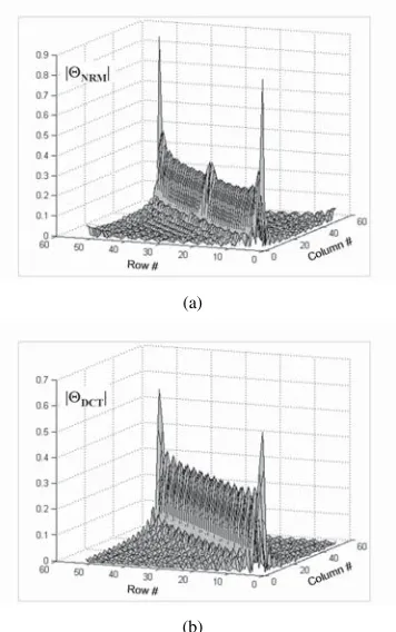
The problem in fact is more complex than this, since in a real scenario not all N carriers are data-bearing sub-carriers. An example is the 802.11a standard, where onlyNu out of N sub-carriers contain information, withNu = 52 and N = 64. In this case the NRM cannot be obtained as in (10), since now the vectorHˆlis a column vector withNuelements, whereasΘDF T is aN×Nmatrix. A solution for this particular case is provided in [18], yielding aNu×NumatrixΘN RM as follows,
ΘN RM =FH11· F11−F12·F+22·F21
, (12)
with
F+22= FH22·F22+γ2
−1
·FH22, (13)
whereγ is a dummy parameter,0< γ << N−1, used to pre-vent possible numerical instability in the matrix inversion. The matricesF11,F12,F21, andF22are of dimensionsNG×Nu,
NG×(N−Nu),(N−NG)×Nu, and(N−NG)×(N−Nu), respectively, and are made of elements WNnk = N−1
/2 ·
(a)
[image:6.567.64.242.54.338.2](b)
Fig. 5. Noise reduction matrices being considered: (a) Reordered 52×52 DFT-based (ΘNRM); (b) 52×52 DCT-based (ΘDCT).
The matrixF
11corresponds ton∈[0, NG−1](rows 1 to
NG) andk ∈ [N −(Nu/2), N−1]∪[1, Nu/2](columns 1 toNu). F12 corresponds to n∈[0, NG−1](rows 1 toNG)
andk ∈[0]∪[(Nu/2) + 1, N−(Nu/2)−1] (columns 1 to
N−Nu). F21 corresponds to n ∈ [NG, N−1] (rows 1 to
N−NG) andk∈[N−(Nu/2), N−1]∪[1, Nu/2](columns 1 toNu). Finally,F22 corresponds ton∈[NG, N−1](rows 1 toN−NG) and k∈[0]∪[(Nu/2) + 1, N−(Nu/2)−1] (columns 1 toN−Nu). The resulting matrixΘN RM is shown in Fig. 5(a) for the caseN= 64,Nu= 52,NG= 16. It contains 2,704 complex elements, which must be pre-computed and stored. By means ofΘN RM, a noise reduction factor given byυdB = 10·log10(N2/(NG·Nu))can be achieved. In the 802.11a case this reduction is as high as 7 dB. It should be noted that the matrix ΘN RM is fixed once N, Nu and NG have been selected.
The noise reduction concept explained above might be significantly simplified if the NRM is determined not based upon the DFT but on the DCT (Discrete Cosine Transform). Although the DCT is closely related to the DFT, it has a major ability to project energyonto a few transformed coefficients than the DFT has. Nevertheless, according to our design premise,hˆl= IDFT{Hˆl} should have its energy projected onto a few coefficients. As a means to reduce the CTF estimation noise, the pseudo-CIRhˆpseudo,l = IDCT{Hˆl} may be used instead ofˆhl. The DCT-based NRM can be written as
ΘDCT =CH·W ·C, (14)
where C stands for the Nu-point IDCT matrix, CH is the
Nu-point DCT matrix, andW is built as in (11) but now with
dimensions Nu×Nu. In Fig. 5(a)/(b) it can be seen that both matrices, ΘN RM andΘDCT, have a very similar magnitude shape, with their major coefficients concentrated around the main diagonal. Nevertheless, the matrixΘDCT only contains real values whereas ΘN RM is made of complex coefficients. More interestingly, it is not necessary to pre-calculate the matrix ΘDCT, as it is the case for ΘN RM, but we might calculate a forward and reverseNu-point (52-point in case of the IEEE 802.11a standard) DCT on the vector Hˆl in order to reduce the CTF estimation noise.
B. Residual Phase Correction
After FFT calculation and channel correction, a residual phase error remains in the modulated data due to several factors: errors in the estimation of the STO and CFO, Phase Noise, and uncorrected SCFO. When applying the CE algo-rithm it is considered that the transmitted pilots were assigned the values {±1}. Furthermore, the channel is supposed not to change significantly during a period of L OFDM symbols, L being the latency of the CE, so that after channel correction and in the absence of noise the resulting pilots are pure phasors with normalized magnitude given by
Pk,lφ ≈e
j(δ·k+θl), (15)
where δ ∝ L·ξ, θl = L·c0+ (αl−αl−L) and k is the frequency index; ξ is the sampling error (in ppm), αl is the contribution of the Phase Noise (the so-called Common Phase Error) to symboll, andc0is the phase derived from a residual CFO. The method we propose [19], [20] assumes the condition
|δ·k|<< 1 be satisfied ∀k∈ [−26,+26]. In this case (15) may be simplified by considering a first order approximation of the complex exponential, yielding
Pk,lφ = {P φ
k,l}+j· {P φ k,l}
= cos(θl)−δ·k·sin(θl)
+ j(sin(θl) +δ·k·cos(θl)). (16)
In (16) four parameters are of interest namely, cos(θl),
sin(θl), δ·sin(θl), and δ·cos(θl). In order to find these four parameters we must solve the linear system of equations derived from (16) when setting k = −21, −7, +7 and +21, corresponding to the pilot tones. Hence, the parameterscos(θl) andsin(θl)can be found straightforwardly as
cos(θl) = (1/4)·
i=−21,−7,+7,+21
{Pi,lφ},
sin(θl) = (1/4)·
i=−21,−7,+7,+21
{Pi,lφ}. (17a)
δ·sin(θl) = 2
126{P
φ
−21,l}+
3
126{P
φ
−7,l}
− 1263 {P+7φ ,l} − 2
126{P
φ +21,l},
δ·cos(θl) = 2
126{P
φ +21,l}+
3
126{P
φ +7,l}
− 1263 {P−φ7,l} − 2
126{P
φ
−21,l},
which have been modified in order to simplify the scaling by the factor 1/126, yielding
δ·sin(θl)≈ 2
128{P
φ
−21,l}+
3
128{P
φ
−7,l}
− 3
128{P
φ +7,l} −
2
128{P
φ +21,l},
δ·cos(θl)≈ 2
128{P
φ +21,l}+
3
128{P
φ +7,l}
− 3
128{P
φ
−7,l} −
2
128{P
φ
−21,l}. (17b)
The foregoing method saves a significant amount of hard-ware, since neither an arctangent block nor an NCO is needed for RPE estimation and correction, respectively.
IV. THEDIGITALTIMINGLOOP
The general scheme of the IRx shown in Fig. 1 includes a so-called Digital Timing Loop (DTL). The purpose of the DTL is to estimate and correct the SCFO. Each OFDM symbol is composed of 80 samples, before CP extraction and FFT operation, with a sampling rate fs = 20 MHz. In the case of a sampling oscillator with e.g. 20 ppm frequency error, this turns into fs = 20,000,400 Hz. Thus 80.0016 samples are obtained for the initial symbol instead of exactly 80, i.e. a timing error of 0.0016 samples. This timing error is not fixed, but it will be 0.0032 samples for the second symbol, 0.0048 for the third one and so on. In essence, the SCFO will be observed as a dynamic timing error that has to be monitored throughout reception. Considering the case of a 6 Mbps transmission, the 802.11a standard allows a frame length of up to 1,367 data symbols, which means that the last OFDM symbol will be affected by a timing error of about 2.2 samples. In our consideration the total SCFO may be as high as 80 ppm (combining the effects from Tx and Rx), yielding a maximum accumulated timing error of 8.8 samples. Since the timing error appears as a linear phase after FFT operation, pilots are very well suited to estimate it. The method shown in the foregoing section for RPE estimation and correction isa posteriori, i.e. no attempt is done to correct the main sources causing the phase error, but only the phase error itself. Hence, we need not only a method to estimate the SCFO based on the pilots but also a way to correct for it prior to FFT operation in order to avoid ICI.
A. Timing Error Discriminator
In a first stage, the variable timing error must be estimated. In the estimation we make use of the phase error signal provided by the RPE estimator, i.e.Pk,lφ in (15). The estimator is based on a solution proposed by Yang in [21], in which two reference sequences are defined, namely
Cp,learlyˆ=ejNπ·p,
Cp,llateˆ=e− jπ
N·p, (18)
wherep corresponds to the pilot sub-carrier position and lis the symbol index.
The RPE signalPk,lφ is compared with these two references through correlation, thus yielding
a(l) =|Rlate(l)|2− |Rearly(l)|2, (19)
with
Rearly(l) = P−1
i=0
Ppφ
0+i·Δ,l· C early p0+i·Δ,l
∗
≈ P−1
i=0
ej2Nπ·(p0+i·Δ)·(Δtl−12) +V
early(l),
Rlate(l) = P−1
i=0
Ppφ
0+i·Δ,l·
Cplate0+i·Δ,l ∗
≈ P−1
i=0
ej2Nπ·(p0+i·Δ)·(Δtl+12) +V
late(l), (20)
whereVearly(l)andVlate(l)are Gaussian noise components. In (20) it has been considered that pilot sub-carriers are at positionp =p0 +i·Δ, with0≤i≤P−1,Pbeing the total number of pilots per OFDM symbol, andΔthe pilot distance. The approximation done in (20) applies whenPk,lφ adheres to the approximation in (15). The total timing error (in samples) at symbol lin (20) is
Δtl=
tθ−ˆtθ,l
+ξ·L·(N +NG), (21)
wheretθis a residual timing synchronization error (|tθ|<0.5 samples),ˆtθ,l is an estimation oftθat symboll, and ξstands for the SCFO (in ppm). In (20) it is further considered that
|Δtl| ≤0.5. After low-pass filtering (19), we finally obtain the timing discriminator as follows (sub-indexlhas been omitted for clarity)
S(Δt) =
sinNπ ·P·Δ·Δt+12 sinNπ ·Δ·Δt+12
2
− sin
π
N ·P·Δ·
Δt−12
sinNπ ·Δ·Δt−12
2
, (22)
whereP= 4,Δ = 14 andN = 64 in the 802.11a case.
B. Timing Error Correction
The parameter of interest is the relative error existing between the sampling period Ts at the Analog-to-Digital converters (ADC), and the corrected (ideal) sampling timeTI, i.e.TI/Ts=1 +ξ. These two sampling periods are related as follows,
with
mi=i·TI+τI·TI, (24)
where0≤μi<1is thefractional delay,mi is thebasepoint, iis the discrete timing variable after timing correction (integer value), whereas τI represents a fractional part of TI. The function x rounds x to the nearest integer towards minus infinity. The timing error compensation is driven by a control block (see Fig. 1), which contains acontrol word,w(l). This parameter is updated on a symbol basis, i.e. every 4μs, and provides the latest estimate of the ratioTI/Tsas follows,
w(l+ 1) =w(l) +Kw·e(l), (25)
with
e(l+ 1) =e(l) +Ke·a(l), (26)
beinga(l)as in (19). The parameterKedefines the bandwidth of the low-pass filter in (26) and it was selected to be 0.01. The parameter Kw is given as Kw = (2·Smax·(N+NG))−1, whereSmaxis the maximum value of S(Δt)in (22).
The parametersmi andμi used in the variable interpolator will be recursively computed as explained in [7, page 523]. We already expressedi·TI+τI·TI as a function of (mi,μi) in (23). The next sample(i+ 1)·TI+τI·TI is given by
(i+ 1)·TI+τI ·TI =mi·Ts+
μi+
TI
Ts
·Ts. (27)
By replacing in (27) the unknown ratio (TI / Ts) by its estimatew(mi)we obtain
(i+ 1)·TI+τI·TI = mi·Ts
+ μi+w(mi) ·Ts
+ [μi+w(mi)]mod1·Ts. (28)
From the previous, it readily follows the recursion for the estimates,
mi+1= mi+μi+w(mi),
μi+1= [μi+w(mi)]mod1. (29)
In order to obtain the value forμibased on the control word
w(mi)we define the function
η(mi, d) ˆ=μi+w(mi)−d, (30)
withd = 0, 1, 2, ...
At the basepointmi the value η(mi,0) is stored in a b -bit register. At every Ts cycle the value of the register is decremented by 1, i.e.
η(mi, d+ 1) =η(mi, d)−1. (31)
As long asη(mi, d)>1, there obviously exists an integer μi+w(mi)> mi+d. The criterion to obtain the next base-pointmi+1 is η(mi, dmin)<1, where dmin is the smallest integer for which the condition is fulfilled. Thus, the decrease
operation is continued until the condition η(mi, dmin) < 1 is detected. By definition, the register content η(mi, dmin) equals μi+1. Afterwards, the operations are continued for
mi+1 with the initial value
η(mi+1,0) =η(mi, dmin) +w(mi+1). (32)
The timing error correction block in Fig. 1 is based on a first order Lagrange polynomial interpolator and makes use of a Farrow structure [7], [22]. Higher order interpolators cannot be used since the DTL becomesunstable. The reason for this instability is related to the considerations made in (16) for calculation of Pk,lφ , which no longer hold when high order interpolators are used.
V. SIMULATIONRESULTS
This section analyzes the performance of the synchronizer, the CE and the DTL under different transmit conditions through extensive computer simulations. We already men-tioned in Section II that the synchronizer was mainly affected by the AGC. Since the attenuation suffered by the transmitted OFDM frame is unknown to the receiver, an AGC able to apply a variable amplification is mandatory prior to ADC. The AGC should be capable of keeping the signal inside a certain voltage range given by the bias voltage of the ADCs. The frame detector found in the synchronizer should be robust against two main effects caused by the AGC:
1) Since the AGC is not able to distinguish the signal of interest from the noise, in the absence of any signal the noise will be amplified in the worst case to the voltage limits of the ADCs. These high noise levels should not provoke false frame detections.
2) In a high SNR situation, the AGC has to change very quickly from a high amplification level to a lower one when the signal is received. Since the AGC cannot react instantaneously to sudden changes in the input power level, the AGC output signal will be heavily saturated for a certain time.
(a) (b)
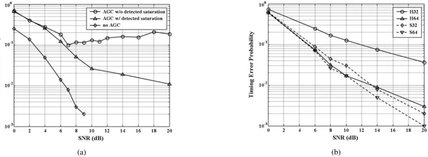
Fig. 6. Simulation results for the synchronizer (channel A,= 1.2): (a) Simulated FAP for the frame detector; (b) Simulated TEP at the output of the crosscorrelator.
the SNR increases. Nevertheless, since saturation is easily detectable at the ADC, the previous effect can be highly mitigated by setting to zero all those saturated samples before being delivered to the frame detector. The obtained standard deviation for the normalized frequency offset estimator shows no dependency on the AGC and has a minimum bound of 0.01, i.e. 1% of the sub-carrier spacing. This value helps in determining the number of bits necessary to represent the frequency offset in the arctangent calculator used in the synchronizer. Finally, Fig. 6(b) depicts the Timing Error Probability (TEP) derived from the crosscorrelator. Symbol timing is provided by the position of the first significant peak coming out from the crosscorrelator. The ideal position of the peak, i.e. m1 in Fig. 2, is known beforehand and a timing error occurs when the estimated position of the peak differs in more than±2 samples from the ideal position. Nevertheless this definition of the timing error only makes sense if the CP of the symbol being received immediately after the preamble symbols is considered to be 14 samples long instead of 16 in order to compensate positive timing errors. Four possible versions of the crosscorrelator have been tested depending on the length of the reference signalcREF(m), either 32 or 64 samples, and the type of multiplier, either 1-bit XNOR-based multipliers (Hard crosscorrelator) or floating point multipliers (Soft crosscorrelator) with the number of bits determined by the computer on which the simulation is being run. Results shown in Fig. 6(b) indicate that the selection of a 32-sample H-crosscorrelator may not be appropriate and should be increased to 64 samples. Despite of these results, our first version of the synchronizer considers only a reference of 32 samples in order to reduce the signal processing latency as much as possible.
Fig. 7 depicts the Mean-Square Error (MSE) performance of the proposed channel estimator considering all data rates defined for the 802.11a standard. Channel models A and D [23] are considered in the simulations. Channel D corresponds to a Line-Of-Sight (LOS) channel with a maximum delay spread of 1,050 ns (140 ns rms). In both cases a Doppler frequency of 58 Hz (v= 3 m/s,FC = 5,805 MHz) was used. In order to smooth the simulation results, we firstly tested 20 different seeds and looked for the one representing an average channel. This seed was used afterwards for the MSE estimation. Each point in Fig. 7 is obtained after averaging
the MSE in 10 trials where a frame containing 37 OFDM data symbols is transmitted at each trial. Furthermore, six soft bits were used during demodulation together with a traceback length of 50 bits in the Viterbi decoder. In order to reduce complexity, a hard-output Viterbi decoder was considered. The figures show a substantial improvement in the MSE when a LOS channel is present. The abrupt decrease of the MSE indicates the point from which on the Viterbi decoder is able to provide fully correct output bits. The correctness of these bits is crucial in order to assure the stability of the CE, specially at the higher transmission rates. Furthermore, Fig. 7 also shows that it will be extremely difficult to obtain the maximum data rates (48 and 54 Mbps) in a real wireless channel, even with LOS, since these rates require a SNR well above 30 dB. The standard 802.11a [1] specifies a Packet Error Rate (PER) of 10% measured on 1000-byte frames, which is equivalent to a BER = 1.25e-5. Fig. 8 shows the results of our Monte-Carlo BER simulations based on 1000-byte frames. The same channel seed as in Fig. 7 was used in Fig. 8. It can be seen from Fig. 8 that the higher modulation schemes require very high SNR in order to achieve the minimum BER and we may use them only in very limited scenarios.
5 10 15 20 25 30 35 40 10−4
10−3 10−2
10−1 100
101
SNR (dB)
MSE
6 Mbps, Channel A 9 Mbps, Channel A 6 Mbps, Channel D 9 Mbps, Channel D
(a)
10 15 20 25 30 35 40 10−2
10−1 100
101
SNR (dB)
MSE
12 Mbps, Channel A 18 Mbps, Channel A 12 Mbps, Channel D 18 Mbps, Channel D
(b)
10 15 20 25 30 35 40 10−2
10−1 100 101
SNR (dB)
MSE
24 Mbps, Channel A 36 Mbps, Channel A 24 Mbps, Channel D 36 Mbps, Channel D
(c)
15 20 25 30 35 40 45 50 55 10−2
10−1 100 101
SNR (dB)
MSE
48 Mbps, Channel A 54 Mbps, Channel A 48 Mbps, Channel D 54 Mbps, Channel D
[image:10.567.63.502.46.372.2](d)
Fig. 7. MSE versus SNR for the proposed modified CD3 channel estimator according to the 802.11a standard: (a) BPSK modulation schemes; (b) QPSK modulation schemes; (c) 16-QAM modulation schemes; (d) 64-QAM modulation schemes.
VI. CONCLUSION
We have investigated the implementation of the Inner Receiver of an OFDM-WLAN system based on the IEEE 802.11a standard. Solutions for the most critical blocks, i.e. Synchronizer, Channel Estimator and Digital Timing Loop, have been proposed and analyzed under careful consideration of nearly realistic transmit conditions. Hence, although our investigations reveal that the Synchronizer is strongly influ-enced by the gain control, the proposed architecture is shown to be relatively robust against the AGC effects. Regarding the Channel Estimator, a decision-directed architecture has been examined. Two novel solutions have been incorporated into the design in order to improve the performance. Firstly, a novel DCT-based noise reduction filter exploits the energy compression capabilities of the DCT as a means to reduce the channel estimation noise with a moderate computational load. Secondly, the residual phase error is eliminated by means of an innovative estimator that extremely simplifies the traditional solution based on arctangent plus NCO operation. In order to derive a simple time tracking algorithm we have made use of concepts already established in the literature. However, the way these concepts are applied to an OFDM receiver is novel in our solution. The proposed solution has proven to be applicable in both LOS and NLOS channels. However, the performance of the DTL is limited by the fact that only first order Farrow interpolators assure stability of the algorithm.
Fig. 9. EVM versus SNR considering the proposed variable timing estimator for 12 Mbps (channel A), and 54 Mbps (channel D) withξ=−80ppm.
ACKNOWLEDGMENT
[image:10.567.298.531.418.602.2]2 4 6 8 10 12 14 16 18 10−6
10−5
10−4 10−3 10−2
10−1 100
SNR (dB)
BER
6 Mbps, Channel A 9 Mbps, Channel A 6 Mbps, Channel D 9 Mbps, Channel D PER = 10%
(a)
5 7 9 11 13 15 17 19 21 23 25 10−6
10−5
10−4 10−3 10−2
10−1 100
SNR (dB)
BER
12 Mbps, Channel A 18 Mbps, Channel A 12 Mbps, Channel D 18 Mbps, Channel D PER = 10%
(b)
12 14 16 18 20 22 24 26 28 30 32 34 36 38 40 10−6
10−5 10−4 10−3 10−2 10−1 100
SNR (dB)
BER
24 Mbps, Channel A 36 Mbps, Channel A 24 Mbps, Channel D 36 Mbps, Channel D PER = 10%
(c)
26 28 30 32 34 36 38 40 42 44 46 48 50 10−6
10−5 10−4 10−3 10−2 10−1 100
SNR (dB)
BER 48 Mbps, Channel A 54 Mbps, Channel A 48 Mbps, Channel D 54 Mbps, Channel D PER = 10%
[image:11.567.71.504.51.367.2](d)
Fig. 8. BER versus SNR for the proposed modified CD3 channel estimator according to the 802.11a standard: (a) BPSK modulation schemes; (b) QPSK modulation schemes; (c) 16-QAM modulation schemes; (d) 64-QAM modulation schemes.
REFERENCES
[1] “Wireless LAN medium access control (MAC) and physical layer (PHY) specifications: High speed physical layer in the 5 GHz band,” IEEE P802.11a/D7.0, Part II, 1999.
[2] “Wireless LAN medium access control (MAC) and physical layer (PHY) specifications. Amendment 4: Further higher data rate extension in the 2.4 GHz band,” IEEE 802.11G. Standard for IT - Telecommunications and information exchange between systems LAN/MAN - Part II, 2003. [3] [Online.] Available: www.wigwam-project.com
[4] [Online.] Available: www.multibandofdm.org
[5] M. Speth, S. A. Fechtel, G. Fock, and H. Meyr, “Optimum receiver design for wireless broad-band systems using OFDM - Part I,” IEEE Trans. Commun., vol. 47, no. 11, pp. 1668–1677, Nov. 1999. [6] P. Robertson and S. Kaiser, “Analysis of the effects of phase-noise in
orthogonal frequency division multiplex (OFDM) systems,” in Proc. IEEE ICC, June 1995, pp. 1652–1657.
[7] H. Meyr, M. Moeneclaey, and S. Fechtel, Digital Communication Receivers: Synchronization, Channel Estimation, and Signal Processing. New York: Wiley, 1998.
[8] M. Krsti´c, A. Troya, K. Maharatna, and E. Grass, “Optimized low-power synchronizer design for the IEEE 802.11a standard,” in Proc. IEEE ICASSP, Apr. 2003, vol. 2, pp. 333–336.
[9] A. Troya, K. Maharatna, M. Krsti´c, and E. Grass, “Method and device for frame detection and synchronizer.” PCT Patent WO 2004/008706 A2, pending, Jan. 22, 2004.
[10] K. Maharatna, A. Troya, S. Banerjee, and E. Grass, “A CORDIC like processor for computation of arctangent and absolute magnitude of a vector,” inProc. IEEE ISCAS, May 2004, vol. 2, pp. 713–716. [11] K. Maharatna, A. Troya, S. Banerjee, E. Grass, and M. Krsti´c, “A 16-bit
CORDIC rotator for high-speed wireless LAN,” inProc. IEEE PIMRC, Sep. 2004, vol. 3, pp. 1747–1751.
[12] K. Maharatna, S. Banerjee, E. Grass, M. Krsti´c, and A. Troya, “Modified virtually scaling-free CORDIC rotator algorithm and architecture,”IEEE Trans. Circuits Syst. Video Technol., vol. 15, no. 11, pp. 1463–1474, Nov. 2005.
[13] T. M. Schmidl and D. C. Cox, “Robust frequency and timing synchro-nization for OFDM,”IEEE Trans. Commun., vol. 45, no. 12, pp. 1613– 1621, Dec. 1997.
[14] B. Stantchev and G. Fettweis, “Burst synchronization for OFDM-based cellular systems with separate signaling channel,” inProc. IEEE VTC, May 1998, pp. 758–762.
[15] V. Mignone and A. Morello, “CD3-OFDM: A novel demodulation scheme for fixed and mobile receivers,” IEEE Trans. Commun., vol. 44, no. 9, pp. 1144–1151, Sep. 1996.
[16] J.-J. van de Beek, O. Edfors, M. Sandell, S. K. Wilson, and P. O. Bör-jesson, “On channel estimation in OFDM systems,” inProc. IEEE VTC, July 1995, vol. 2, pp. 815–819.
[17] O. Edfors, M. Sandell, J.-J. van de Beek, S. K. Wilson, and P. O. Bör-jesson, “OFDM channel estimation by singular value decomposition,” IEEE Trans. Commun., vol. 46, no. 7, pp. 931–939, July 1998. [18] H. Schmidt, V. Kühn, K.-D. Kammeyer, R. Rueckriem, and S. Fechtel,
“Channel tracking in wireless OFDM systems,” in Proc. 5th World Multi-Conference on Systemics, Cybernetics and Informatics, July 2001, vol. 4, pp. 402–406.
[19] A. Troya, M. Krsti´c, and K. Maharatna, “Simplified residual phase correction mechanism for the IEEE 802.11a standard,” inProc. IEEE VTC-Fall, Oct. 2003, vol. 2, pp. 1137–1141.
[20] A. Troya, K. Maharatna, and M. Krsti´c, “Verfahren und Vorrichtung zur Fehlerkorrektur von Multiplex-Signalen.” PCT Patent WO 2004/036863 A1, pending, Apr. 29, 2004.
[21] B. Yang, K. B. Letaief, R. S. Cheng, and Z. Cao, “An improved combined symbol and sampling clock synchronization method for OFDM systems,” inProc. IEEE Wireless Commun. Networking Conf., Sep. 1999, vol. 3, pp. 1153–1157.
[22] L. Erup, F. M. Gardner, and R. A. Harris, “Interpolation in digital modems - Part II: Implementation and performance,” IEEE Trans. Commun., vol. 41, no. 6, pp. 998–1008, June 1993.
Alfonso Troya (M’95) was born in Barcelona, Spain, in 1975. He received the M.Sc. degree in Telecommunications Engineering from the Techni-cal University of Catalonia, Barcelona, Spain, in 1999, and the Dr.-Ing. degree from Brandenburg University of Technology, Cottbus, Germany, in 2004.
He joined the IHP (Institute for High Performance microelectronics), Frankfurt (Oder), Germany, in 1999, as a Research Associate in the Wireless Com-munication Systems Department, where he worked on the development and implementation of digital signal processing algo-rithms for broadband wireless communication systems. In October 2004 he joined Infineon Technologies AG, Munich, Germany, as an Algorithm Concept Engineer. He is currently involved in the development of OFDM-based communication systems and their implementation on Software-Defined Radio architectures.
Dr. Troya is a member of the IEEE Signal Processing Society.
Koushik Maharatna(M’02) received the M.Sc. de-gree in Electronic Science from Calcutta University, Calcutta, India, in 1995 and the Ph.D. degree from Jadavpur University, Calcutta, India, in 2002. From 1996 to 2000, he was involved in projects sponsored by the Government of India undertaken at the In-dian Institute of Technology (IIT), Kharagpur, India. From 2000 to 2003, he was a Research Scientist with IHP, Frankfurt (Oder), Germany. During this phase, his main involvement was related to the design of a single-chip modem for the IEEE 802.11a standard. In August 2003, he joined the Department of Electrical & Electronics Engineering, University of Bristol, Bristol, UK as a Lecturer. From October 2006 he is with the School of Electronics and Computer Science, University of Southampton, where he is currently a Senior Lecturer. His research interests include development of VLSI architectures for the application in DSP and communication, computer arithmetic, low-power design, and analog signal processing.
Dr. Maharatna has served as session chair for IEEE ISCAS 2005 and VLSI design Conference 2006, and also acted as a reviewer for several IEEE Journals and Conferences. He is currently a member of the Engineering and Physical Research Council (EPSRC) college in the UK. He is a member of the IEEE Circuits and Systems Society.
Milo˘s Krsti´c was born in Niˇs, Serbia, in 1973. He received the Dipl.-Ing. and the M.Sc. degrees in Electronics from the University of Niˇs, Serbia, in 1997 and 2001, respectively, and the Dr.-Ing. degree from Brandenburg University of Technology, Cottbus, Germany, in 2006.
Since 2001 he has been with IHP, Frankfurt (Oder), Germany, as a Research Associate within the Wireless Communication Systems Department, where he is currently working on low-power digi-tal design techniques for wireless applications and globally-asynchronous locally-synchronous (GALS) methodologies for digital systems integration.
Eckhard Grass received his Dr.-Ing. degree in Electronics from the Humboldt University, Berlin, Germany, in 1992.
He worked as a Visiting Research Fellow at Loughborough University (U.K.) from 1993 to 1995 and as a Senior Lecturer in Microelectronics at the University of Westminster, London, U.K., from 1995 to 1999. He has been with IHP, Frankfurt (Oder), Germany, since 1999, where he currently leads a project on the development and implementation of a wireless broadband communication system in the 60 GHz band. His research interests include data-driven (asynchronous) signal processing structures and low-power VLSI implementation of communication systems.
Ulrich Jagdhold received the Diploma in Physics (M.Sc. degree) from the Technical University of Dresden, Dresden, Germany, in 1987. From 1987 to 1996, he was with the Technology Integration Group of the IHP, Frankfurt (Oder), Germany, working on CMOS, BiCMOS, and SiGe technologies and device physics. In 1997 he joined the Wireless Communication Systems Department of IHP, where he has been working on WLAN system development projects, focusing on baseband integration issues and ASIC design, including development of digital CMOS libraries.
Rolf Kraemer (M’79) received his Diploma and Ph.D. degrees in Electrical Engineering and Com-puter Science from the RWTH Aachen, Germany, in 1979 and 1985, respectively. He has worked for 15 years in R&D of communication and multimedia systems at Philips Research Laboratories in Ham-burg and Aachen. Since 1998 he is a professor of systems at the Brandenburg University of Technol-ogy, Cottbus, Germany. He also leads the Wireless Communications Systems Department of the IHP, where his research focus is on wireless Internet systems spanning from application down to Systems-on-Chip. He is co-founder of the startup company lesswire AG, where he holds the position of the CTO.