12.1
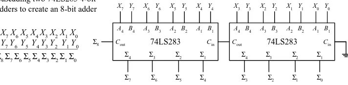
The Basics of Digital Electronics
Until now I have mainly covered the analog realm of electronics—circuits that accept and respond to voltages that vary continuously over a given range. Such analog cir-cuits included rectifiers, filters, amplifiers, simple RC timers, oscillators, simple tran-sistor switches, etc. Although each of these analog circuits is fundamentally important in its own right, these circuits lack an important feature—they cannot store and process bits of information needed to make complex logical decisions. To incorporate logical decision-making processes into a circuit, you need to use digital electronics.
12.1.1
Digital Logic States
In digital electronics there are only two voltage states present at any point within a circuit. These voltage states are either high or low. The meaning of a voltage being high or low at a particular location within a circuit can signify a number of things. For example, it may represent the on or off state of a switch or saturated transistor. It may represent one bit of a number, or whether an event has occurred, or whether some action should be taken.
The high and low states can be represented as true and false statements, which are used in Boolean logic. In most cases, high =true and low =false. However, this does not have to be the case—you could make high =false and low =true. The decision to use one convention over the other is a matter left ultimately to the designer. In digi-tal lingo, to avoid people getting confused over which convention is in use, the term
Digital Electronics
HIGH (H), or 1 +5V
0V
LOW (L), or 0
continuous voltage waveform
Analog Signal Digital Signal
discrete voltage levels
+5V
10K
+5V
10K
+5V 0V
Using a switch to demonstrate logic states
HIGH (logic 1)
LOW (logic 0)
313
FIGURE 12.1
positive true logic is used when high =true, while the term negative true logic is used when high =false.
In Boolean logic, the symbols 1 and 0 are used to represent true and false, respec-tively. Now, unfortunately, 1 and 0 are also used in electronics to represent high and low voltage states, where high =1 and low =0. As you can see, things can get a bit confusing, especially if you are not sure which type of logic convention is being used, positive true or negative true logic. I will give some examples later on in this chapter that deal with this confusing issue.
The exact voltages assigned to a high or low voltage states depend on the specific logic IC that is used (as it turns out, digital components are entirely IC based). As a general rule of thumb, +5 V is considered high, while 0 V (ground) is considered low. However, as you will see in Section 12.4, this does not have to be the case. For exam-ple, some logic ICs may interrupt a voltage from +2.4 to +5 V as high and a voltage from +0.8 to 0 V as low. Other ICs may use an entirely different range. Again, I will discuss these details later.
12.1.2
Number Codes Used in Digital Electronics
Binary
Because digital circuits work with only two voltage states, it is logical to use the binary number system to keep track of information. A binary number is composed of two binary digits, 0 and 1, which are also called bits (e.g., 0 =low voltage, 1 =high voltage). By contrast, a decimal number such as 736 is represented by successive powers of 10:
73610=7 ×10²+3 ×101+6 ×100
Similarly, a binary number such as 11100 (2810) can be expressed as successive powers
of 2:
111002=1 ×24+1 ×23+1 ×22+0 ×21+0 ×20
The subscript tells what number system is in use (X10=decimal number, X2=binary
number). The highest-order bit (leftmost bit) is called the most significant bit (MSB), while the lowest-order bit (rightmost bit) is called the least significant bit (LSB). Meth-ods used to convert from decimal to binary and vice versa are shown below.
It should be noted that most digital systems deal with 4, 8, 16, 32, etc., bit strings. In the decimal-to-binary conversion example given here, you had a 7-bit answer. In
10910 to binary
109/2 = 54 w/ remainder 1 (LSB) 54/2 = 27 w/ remainder 0 27/2 = 13 w/ remainder 1 13/2 = 6 w/ remainder 1 6/2 = 3 w/ remainder 0 3/2 = 1 w/ remainder 1 1/2 = 0 w/remainder 1 (MSB)
Answer: 1101101 8-bit answer: 01101101
Take decimal number and keep dividing by 2, while keeping the remainders. The first remainer becomes the LSB, while the last one becomes the MSB.
Decimal-to-Binary Conversion
10100100 to decimal
1 0 1 0 0 1 0 0
Answer: 16410 Expand the binary number as shown and add up the terms. The result will be in decimal form.
Decimal-to-Binary Conversion
20 21 22 23 24 25 26 27
0 x 20 = 0 0 x 21 = 0 1 x 22 = 4 0 x 23 = 0 0 x 24 = 0 1 x 25 = 32 0 x 26 = 0 1 x 27 = 128
(MSB) (LSB)
an 8-bit system, you would have to add an additional 0 in front of the MSB (e.g., 01101101). In a 16-bit system, 9 additional 0s would have to be added (e.g., 0000000001101101).
As a practical note, the easiest way to convert a number from one base to another is to use a calculator. For example, to convert a decimal number into a binary num-ber, type in the decimal number (in base 10 mode) and then change to binary mode (which usually entails a 2d-function key). The number will now be in binary (1s and 0s). To convert a binary number to a decimal number, start out in binary mode, type in the number, and then switch to decimal mode.
Octal and Hexadecimal
Two other number systems used in digital electronics include the octal and hexadec-imal systems. In the octal system (base 8), there are 8 allowable digits: 0, 1, 2, 3, 4, 5, 6, 7. In the hexadecimal system, there (base 16) there are 16 allowable digits: 0, 1, 2, 3, 4, 5, 6, 7, 8, 9, A, B, C, D, E, F. Here are example octal and hexadecimal numbers with decimal equivalents:
2478(octal) =2 ×82+4 ×81+9 ×80=16710(decimal)
2D516(hex) =2 ×162+D (=1310) ×161+9 ×160=72510(decimal)
Now, binary numbers are of course the natural choice for digital systems, but since these binary numbers can become long and difficult to interpret by our decimal-based brains (a result of our 10 fingers), it is common to write them out in hexadeci-mal or octal form. Unlike decihexadeci-mal numbers, octal and hexadecihexadeci-mal numbers can be translated easily to and from binary. This is so because a binary number, no matter how long, can be broken up into 3-bit groupings (for octal) or 4-bit groupings (for hexadecimal)—you simply add zero to the beginning of the binary number if the total numbers of bits is not divisible by 3 or 4. Figure 12.3 should paint the picture better than words.
Today, the hexadecimal system has essentially replaced the octal system. The octal system was popular at one time, when microprocessor systems used 12-bit and 36-bit words, along with a 6-bit alphanumeric code—all these are divisible by 3-bit units (1 octal digit). Today, microprocessor systems mainly work with 8-bit, 16-bit, 20-bit, 32-bit, or 64-bit words—all these are divisible by 4-bit units (1 hex digit). In other words, an 8-bit word can be broken down into 2 hex digits, a 16-bit word into 4 hex digits, a 20-bit word into 5 hex digits, etc. Hexadecimal representation of binary numbers pops up in many memory and microprocessor applications that use programming
7 1 4
A 3-digit binary number is replaced for each octal digit, and vise versa. The 3-digit terms are then grouped (or octal terms are grouped).
1 0 1 0 1 0 1 1 1
Octal to Binary Binary to Octal
111 001 1002 to octal 1 1 1 0 0 1 1 0 0
Answer: 7148
3E916 to binary 3 E 9
Answer: 0011 1110 10012
A 4-digit binary number is replaced for each hex digit, and vise versa. The 4-digit terms are then grouped (or hex terms are grouped).
0 0 1 1
Hex to Binary Binary to Hex
1001 1111 1010 01112 to octal
Answer: 9FA716 1 1 1 0 1 0 0 1
1 0 0 1 1 1 1 1 1 0 1 0 0 1 1 1
9 F A 7
5378 to binary
5 3 7
Answer: 1010101112
codes (e.g., within assembly language) to address memory locations and initiate other specialized tasks that would otherwise require typing in long binary numbers. For example, a 20-bit address code used to identify 1 of 1 million memory locations can be replaced with a hexadecimal code (in the assembly program) that reduces the count to 5 hex digits. [Note that a compiler program later converts the hex numbers within the assembly language program into binary numbers (machine code) which the microprocessor can use.] Table 12.1 gives a conversion table.
TABLE 12.1 Decimal, Binary, Octal, Hex, BCD Conversion Table
DECIMAL BINARY OCTAL HEXADECIMAL BCD
00 0000 0000 00 00 0000 0000
01 0000 0001 01 01 0000 0001
02 0000 0010 02 02 0000 0010
03 0000 0011 03 03 0000 0011
04 0000 0100 04 04 0000 0100
05 0000 0101 05 05 0000 0101
06 0000 0110 06 06 0000 0110
07 0000 0111 07 07 0000 0111
08 0000 1000 10 08 0001 1000
09 0000 1001 11 09 0000 1001
10 0000 1010 12 0A 0001 0000
11 0000 1011 13 0B 0001 0001
12 0000 1100 14 0C 0001 0010
13 0000 1101 15 0D 0001 0011
14 0000 1110 16 0E 0001 0100
15 0000 1111 17 0F 0001 0101
16 0001 0000 20 10 0001 0110
17 0001 0001 21 11 0001 0111
18 0001 0010 22 12 0001 1000
19 0001 0011 23 13 0001 1001
20 0001 0100 24 14 0010 0000
BCD Code
1 5 0 15010=0001 0101 000(BCD)
0001 0101 000
To convert from BCD to binary is vastly more difficult, as shown in Fig. 12.4. Of course, you could cheat by converting the BCD into decimal first and then convert to binary, but that does not show you the mechanics of how machines do things with 1s and 0s. You will rarely have to do BCD-to-binary conversion, so I will not dwell on this topic—I will leave it to you to figure out how it works (see Fig. 12.4).
BCD is commonly used when outputting to decimal (0–9) displays, such as those found in digital clocks and multimeters. BCD will be discussed later in Section 12.3.
Sign-Magnitude and 2’s Complement Numbers
Up to now I have not considered negative binary numbers. How do you represent them? A simple method is to use sign-magnitude representation. In this method, you simply reserve a bit, usually the MSB, to act as a sign bit. If the sign bit is 0, the num-ber is positive; if the sign bit is 1, the numnum-ber is negative (see Fig. 12.5). Although the sign-magnitude representation is simple, it is seldom used because adding requires a different procedure than subtracting (as you will see in the next section). Occasion-ally, you will see sign-magnitude numbers used in display and analog-to-digital applications but hardly ever in circuits that perform arithmetic.
A more popular choice when dealing with negative numbers is to use 2’s comple-ment representation. In 2’s complecomple-ment, the positive numbers are exactly the same as unsigned binary numbers. A negative number, however, is represented by a binary number, which when added to its corresponding positive equivalent results in zero. In this way, you can avoid two separate procedures for doing addition and subtrac-tion. You will see how this works in the next secsubtrac-tion. A simple procedure outlining how to convert a decimal number into a binary number and then into a 2’s comple-ment number, and vice versa, is outlined in Fig. 12.5.
Arithmetic with Binary Numbers
Adding, subtracting, multiplying, and dividing binary numbers, hexadecimal num-bers, etc., can be done with a calculator set to that particular base mode. But that’s
Weighting factor bit position decimal binary
a 1 1
b 2 10
c 4 100
d 8 1000
e 10 1010
f 20 10100
g 40 101000
h 80 1010000
i 100 1100100
j 200 11001000
k 400 110010000
l 800 1100100000
0110 0011
6 3
0001 0010 10100 101000 111111 +
1000 0010
8 2
0011 3
0001 0010 10100 1100100000 1100110111 +
3-digit BCD
MSD Second digit LSD
l k j i h g f e d c b a
2
0
x 100
2
1
x 100
2
2
x 100
2
3
x 100 2 x 10 3 x 10² 2 2 x 10 1 x 10² 0 2 x 1 3 x 12 2 x 12 0 2 x 1 1
(decimal)
(BCD)
(binary)
cheating, and it doesn’t help you understand the “mechanics” of how it is done. The mechanics become important when designing the actual arithmetical circuits. Here are the basic techniques used to add and subtract binary numbers.
ADDING
Adding binary numbers is just like adding decimal numbers; whenever the result of adding one column of numbers is greater than one digit, a 1 is carried over to the next column to be added.
SUBTRACTION
Subtracting decimal numbers is not as easy as it looks. It is similar to decimal subtraction but can be confusing. For example, you might think that if you were to subtract a 1 from a 0, you would borrow a 1 from the column to the left. No! You must borrow a 10 (210). It becomes a headache
if you try to do this by hand. The trick to subtracting binary numbers is to use the 2’s complement representation that provides the sign bit and then just add the positive number with the negative number to get the sum. This method is often used by digital circuits because it allows both addition and subtraction, without the headache of having to subtract the smaller number from the larger number.
ASCII
ASCII (American Standard Code for Information Interchange) is an alphanumeric code used to transmit letters, symbols, numbers, and special nonprinting characters between computers and computer peripherals (e.g., printer, keyboard, etc.). ASCII consists of 128 different 7-bit codes. Codes from 000 0000 (or hex 00) to 001 1111 (or hex 1F) are reserved for nonprinting characters or special machine commands like ESC (escape), DEL (delete), CR (carriage return), LF (line feed), etc. Codes from 010 0000 (or hex 20) to 111 1111 (or hex 7F) are reserved for printing characters like a, A, #, &, {, @, 3, etc. See Tables 12.2 and 12.3. In practice, when ASCII code is sent, an additional bit is added to make it compatible with 8-bit systems. This bit may be set to 0 and ignored, it may be used as a parity bit for error detection (I will cover parity bits in Section 12.3), or it may act as a special function bit used to implement an additional set of specialized characters.
Decimal, Sign-Magnitude, 2’s Complement Conversion Table
SIGN-DECIMAL MAGNITUDE 2’S COMPLEMENT
+7 0000 0111 0000 0111
+6 0000 0110 0000 0110
+5 0000 0101 0000 0101
+4 0000 0100 0000 0100
+3 0000 0011 0000 0011
+2 0000 0010 0000 0010
+1 0000 0001 0000 0001
0 0000 0000 0000 0000
−1 1000 0001 1111 1111
−2 1000 0010 1111 1110
−3 1000 0011 1111 1101
−4 1000 0100 1111 1100
−5 1000 0101 1111 1011
−6 1000 0110 1111 1010
−7 1000 0111 1111 1001
−8 1000 1000 1111 1000
Decimal to 2's complement
If the decimal number is positive, the 2's complement number is equal to the true binary equivalent of the decimal number.
If the decimal number is negative, the 2's complement number is found by:
1) Complementing each bit of the true binary equivalent of the decimal (making 1's into 0's and vise versa). This is is called taking the 1's complement. 2) Adding 1 to the 1's complement number to get the magnitude bits. The sign bit will always end up being 1.
2's complement to decimal If the 2's complement number is positive (sign bit = 0), perform a regular binary-to-decimal conversion. If the 2's complement number is negative (sign bit = 1), the decimal sign will be negative. The decimal is found by:
1) Complementing each bit of the 2's complement number.
2) Adding 1 to get the true binary equivalent. 3) Performing a true binary-to-decimal conversion. 1100 1101 (2's comp) to decimal
2's comp = 1100 1101 Complement = 0011 0010 Add 1 = +1 True binary = 0011 0011 Decimal eq. = – 5110
– 4110 to 2's complement true binary = 0010 1001 + 410 to 2's complement
2's comp = 0010 1001
true binary = 0010 1001 1's comp = 1101 0110 Add 1 = +1 2's comp = 0010 1001
0 1 0 1 0 0 1 1 1 0 0 0
1 1 1 510 = 310 =
+ 2010 = 0 0 0 1 0 1 0 0
8710 = 0 1 0 1 0 1 1 1 0 1 1 0 1 0 1 1 +
0 1 0 0 0 0 0 1 0 0 1 1 _
10 10 0
1
410 110 310 _
Subtraction done the long way
+1910 = 0 0 0 1 0 0 1 1 - 710 = 1 1 1 1 1 0 0 1 Sum = 0 0 0 0 1 1 0 0 2's comp. subtraction
FIGURE 12.5
DEC HEX 7-BIT CODE CONTROL CHAR CHAR MEANING DEC HEX 7-BIT CONTROL CHAR CHAR MEANING
00 00 000 0000 ctrl-@ NUL Null 16 10 001 0000 ctrl-P DLE Data line escape 01 01 000 0001 ctrl-A SOH Start of heading 17 11 001 0001 ctrl-Q DC1 Device control 1 02 02 000 0010 ctrl-B STX Start of text 18 12 001 0010 ctrl-R DC2 Device control 2 03 03 000 0011 ctrl-C ETX End of text 19 13 001 0011 ctrl-S DC3 Device control 3 04 04 000 0100 ctrl-D EOT End of xmit 20 14 001 0100 ctrl-T DC4 Device control 4 05 05 000 0101 ctrl-E ENQ Enquiry 21 15 001 0101 ctrl-U NAK Neg acknowledge 06 06 000 0110 ctrl-F ACK Acknowledge 22 16 001 0110 ctrl-V SYN Synchronous idle 07 07 000 0111 ctrl-G BEL Bell 23 17 001 0111 ctrl-W ETB End of xmit block 08 08 000 1000 ctrl-H BS Backspace 24 18 001 1000 ctrl-X CAN Cancel
09 09 000 1001 ctrl-I HT Horizontal tab 25 19 001 1001 ctrl-Y EM End of medium 10 0A 000 1010 ctrl-J LF Line feed 26 1A 001 1010 ctrl-Z SUB Substitute 11 0B 000 1011 ctrl-K VT Vertical tab 27 1B 001 1011 ctrl-[ ESC Escape 12 0C 000 1100 ctrl-L FF Form feed 28 1C 001 1100 ctrl-\ FS File separator 13 0D 000 1101 ctrl-M CR Carriage return 29 1D 001 1101 ctrl-] GS Group separator 14 0E 000 1110 ctrl-N S0 Shift out 30 1E 001 1110 ctrl-^ RS Record separator 15 0F 000 1111 ctrl-O SI Shift in 31 1F 001 1111 ctrl-_ US Unit separator
TABLE 12.3 ASCII Printing Characters
DEC HEX 7-BIT CODE CHAR DEC HEX 7-BIT CHAR DEC HEX 7-BIT CODE CHAR
32 20 010 0000 SP 64 40 100 0000 @ 96 60 110 0000 ’
33 21 010 0001 ! 65 41 100 0001 A 97 61 110 0001 a
34 22 010 0010 “ 66 42 100 0010 B 98 62 110 0010 b
35 23 010 0011 # 67 43 100 0011 C 99 63 110 0011 c
36 24 010 0100 $ 68 44 100 0100 D 100 64 110 0100 d
37 25 010 0101 % 69 45 100 0101 E 101 65 110 0101 e
38 26 010 0110 & 70 46 100 0110 F 102 66 110 0110 f
39 27 010 0111 ‘ 71 47 100 0111 G 103 67 110 0111 g
40 28 010 1000 ( 72 48 100 1000 H 104 68 110 1000 h
41 29 010 1001 ) 73 49 100 1001 I 105 69 110 1001 i
42 2A 010 1010 * 74 4A 100 1010 J 106 6A 110 1010 j
43 2B 010 1011 + 75 4B 100 1011 K 107 6B 110 1011 k
44 2C 010 1100 , 76 4C 100 1100 L 108 6C 110 1100 l
45 2D 010 1101 - 77 4D 100 1101 M 109 6D 110 1101 m
46 2E 010 1110 . 78 4E 100 1110 N 110 6E 110 1110 n
47 2F 010 1111 / 79 4F 100 1111 O 111 6F 110 1111 o
48 30 011 0000 0 80 50 101 0000 P 112 70 111 0000 p
49 31 011 0001 1 81 51 101 0001 Q 113 71 111 0001 q
50 32 011 0010 2 82 52 101 0010 R 114 72 111 0010 r
51 33 011 0011 3 83 53 101 0011 S 115 73 111 0011 s
52 34 011 0100 4 84 54 101 0100 T 116 74 111 0100 t
53 35 011 0101 5 85 55 101 0101 U 117 75 111 0101 u
54 36 011 0110 6 86 56 101 0110 V 118 76 111 0110 v
55 37 011 0111 7 87 57 101 0111 W 119 77 111 0111 w
56 38 011 1000 8 88 58 101 1000 X 120 78 111 1000 x
57 39 011 1001 9 89 59 101 1001 Y 121 79 111 1001 y
58 3A 011 1010 : 90 5A 101 1010 Z 122 7A 111 1010 z
59 3B 011 1011 ; 91 5B 101 1011 [ 123 7B 111 1011 {
60 3C 011 1100 < 92 5C 101 1100 \ 124 7C 111 1100 |
61 3D 011 1101 = 93 5D 101 1101 ] 125 7D 111 1101 }
62 3E 011 1110 > 94 5E 101 1110 ^ 126 7E 111 1110 ∼
63 3F 011 1111 ? 95 5F 101 1111 _ 127 7F 111 1111 DEL
12.1.3
Clock Timing and Parallel versus Serial Transmission
Before moving on to the next section, let’s take a brief look at three important items: clock timing, parallel transmission, and serial transmission.
Clock Timing
Digital circuits require precise timing to func-tion properly. Usually, a clock circuit that gen-erates a series of high and low pulses at a fixed frequency is used as a reference on which to base all critical actions executed within a sys-tem. The clock is also used to push bits of data through the digital circuitry. The period of a clock pulse is related to its frequency by T=1/f. So, if T=10 ns, then f=1/(10 ns) =100 MHz.
Serial versus Parallel Representation
Binary information can be transmitted from one location to another in either a serial or parallel manner. The serial format uses a single electrical conductor (and a com-mon ground) for data transfer. Each bit from the binary number occupies a separate clock period, with the change from one bit to another occurring at each falling or leading clock edge—the type of edge depends on the circuitry used. Figure 12.9 shows an 8-bit (10110010) word that is transmitted from circuit A to circuit B in 8 clock pulses (0–7). In computer systems, serial communications are used to transfer data between keyboard and computer, as well as to transfer data between two com-puters via a telephone line.
Parallel transmission uses separate electrical conductors for each bit (and a com-mon ground). In Fig. 12.9, an 8-bit string (01110110) is sent from circuit A to circuit B. As you can see, unlike serial transmission, the entire word is transmitted in only one clock cycle, not 8 clock cycles. In other words, it is 8 times faster. Parallel com-munications are most frequently found within microprocessor systems that use multiline data and control buses to transmit data and control instructions from the microprocessor to other microprocessor-based devices (e.g., memory, output regis-ters, etc.).
0 1 2 3 4 5 6 7
+5V 0V
10 ns
f = 1/T = 1/10 ns = 100 MHz T
t
clock V
out
Vout
0 1 2 3 4 5 6 7
0 1 0 0 1 1 0 1
+5V 0V +5V 0V
Circuit A
Circuit A
clock
data
data
LSB MSB
8-bit word
Serial transmission of a 8-bit word (10110010)
a 1
0 1 0 1 0 1 0 1 0 1 0 1 0
b
c
d
e
f
g
1 0
h
LSB
MSB clock
Circuit A
Circuit B
a = 20
b = 21
c = 22
d = 23
e= 24
f = 25
g = 26
h = 27 LSB
MSB
Parallel transmission of a 8-bit word (10110010)
data
data
FIGURE 12.8
12.2
Logic Gates
Logic gates are the building blocks of digital electronics. The fundamental logic gates include the INVERT (NOT), AND, NAND, OR, NOR, exclusive OR (XOR), and exclusive NOR (XNOR) gates. Each of these gates performs a different logical opera-tion. Figure 12.10 provides a description of what each logic gate does and gives a switch and transistor analogy for each gate.
in out in 0 1 out 1 0 Truth table 1 0 + in lamp (out) On = 1 Off = 0
INVERT (NOT) Switch
analogy
Transistor analogy
A NOT gate or inverter outputs a logic level that's the opposite (complement) of the input logic level. Description AND A 1 0 + lamp (out) On = 1 Off = 0 1 0 A B 0 0 1 1 0 1 0 1 0 0 0 1
A B out
The ouput of an AND gate is HIGH only when both inputs are HIGH.
NAND 1 0 + lamp (out) On = 1 Off = 0 1 0 A B 0 0 1 1 0 1 0 1 1 1 1 0
A B out
+5 V A B out 10K 10K 10K
Combines the NOT function with an AND gate; output only goes LOW when both inputs are HIGH. B out A B out 1 0 + lamp (out) On = 1 Off = 0 1 0 A B 0 0 1 1 0 1 0 1 0 1 1 1
A B out
OR A B out +5 V A B out 10K 10K 10K
The output of an OR gate will go HIGH if one or both inputs goes HIGH. The output only goes LOW when both inputs are LOW.
0 0 1 1 0 1 0 1 1 0 0 0
A B out
1 0 +
lamp (out) On = 1 Off = 0 1 0 A B A B out NOR
Combines the NOT function with an OR gate; output goes LOW if one or both inputs are LOW, ouput goes HIGH when both inputs are LOW. out
+5 V
in 10K 10K
Exclusive OR (XOR) Exclusive NOR (XNOR)
0 0 1 1 0 1 0 1 0 1 1 0
A B out
The output of an XOR gate goes HIGH if the inputs are different from each other. XOR gates only come with two inputs.
Combines the NOT function with an XOR gate; output goes HIGH if the inputs are the same. A B out 0 0 1 1 0 1 0 1 1 0 0 1
A B out
A B out +5 V A B out 10K 10K 10K +5 V NOT stage OR stage +5 V A B out 10K 10K 10K +5 V AND stage NOT stage A B out equivalent circuit out A B equivalent circuit
0 = LOW voltage level 1 = HIGH voltage level
12.2.1
Multiple-Input Logic Gates
AND, NAND, OR, and NOR gates often come with more than two inputs (this is not the case with XOR and XNOR gates, which require two inputs only). Figure 12.11 shows a 4-input AND, an 8-input AND, a 3-input NOR, and an 8-input NOR gate. With the 8-input AND gate, all inputs must be high for the output to be high. With the 8-input OR gate, at least one of the inputs must be high for the output to go high.
12.2.2
Digital Logic Gate ICs
The construction of digital gates is best left to the IC manufacturers. In fact, mak-ing gates from discrete components is highly impractical in regard to both overall performance (power consumption, speed, drive capacity, etc.) and overall cost and size.
There are a number of technologies used in the fabrication of digital logic. The two most popular technologies include TTL (transistor-transistor logic) and CMOS (complementary MOSFET) logic. TTL incorporates bipolar transistors into its design, while CMOS incorporates MOSFET transistors. Both technologies perform the same basic functions, but certain characteristics (e.g., power consumption, speed, output drive capacity, etc.) differ. There are many subfamilies within both TTL and CMOS. These subfamilies, as well as the various characteristics associated with each sub-family, will be discussed in greater detail in Section 12.4.
A logic IC, be it TTL or CMOS, typically houses more than one logic gate (e.g., quad 2-input NAND, hex inverter, etc.). Each of the gates within the IC shares a com-mon supply voltage that is implemented via two supply pins, a positive supply pin (+VCCor +VDD) and a ground pin (GND). The vast majority of TTL and CMOS ICs are
designed to run off a +5-V supply. (This does not apply for all the logic families, but I will get to that later.)
Generally speaking, input and output voltage levels are assumed to be 0 V (low) and +5 V (high). However, the actual input voltage required and the actual output voltage provided by the gate are not set in stone. For example, the 74xx TTL series will recognize a high input from 2.0 to 5 V, a low from 0 to 0.8 V, and will guarantee a high output from 2.4 to 5 V and a low output from 0 to 0.4 V. However, for the CMOS 4000B series (VCC= +5 V), recognizable input voltages range from 3.3 to 5 V for high,
0 to 1.7 V for low, while guaranteed high and low output levels range from 4.9 to 5 V and 0 to 0.1 V, respectively. Again, I will discuss specifics later in Section 12.4. For now, let’s just get acquainted with what some of these ICs look like—see Figs. 12.12 and 12.13. [CMOS devices listed in the figures include 74HCxx, 4000(B), while TTL devices shown include the 74xx, 74Fxx, 74LS.]
a b c
e f g h
d out ab
c out
a b c d e f g h
out
a b c
d out
12.2.3
Applications for a Single Logic Gate
Before we jump into the heart of logic gate applications that involve combining logic gates to form complex decision-making circuits, let’s take a look at a few simple applications that require the use of a single logic gate.
Enable/Disable Control
An enable/disable gate is a logic gate that acts to control the passage of a given wave-form. The waveform, say, a clock signal, is applied to one of the gate’s inputs, while 14 13 12 11 10 9 8 1 2 3 4 5 6 7 1A 1B 1Y 2A 2B 2Y GND VCC 4B 4A 4Y 3B 3A 3Y 7400, 74LS00, 74F00, 74HC00, etc.
Quad 2-input NAND 14 13 12 11 10 9 8 1 2 3 4 5 6 7 1Y 1A 1B 2Y 2A 2B GND VCC 4Y 4B 4A 3Y 3B 3A 7402, 74LS02, 74F02, 74HC02, etc.
Quad 2-input NOR 14 13 12 11 10 9 8 1 2 3 4 5 6 7 1A 1Y 2A 2Y 3A 3Y GND VCC 6A 6Y 5A 5Y 4A 4Y 7404, 74LS04, 74F04, 74HC04, etc.
Hex Inverter 14 13 12 11 10 9 8 1 2 3 4 5 6 7 1A 1B 1Y 2A 2B 2Y GND VCC 4B 4A 4Y 3B 3A 3Y 7408, 74LS08, 74F08, 74HC08, etc.
Quad 2-input AND 14 13 12 11 10 9 8 1 2 3 4 5 6 7 1A 1B 2A 2B 2C 2Y GND VCC 1C 1Y 3C 3B 3A 3Y 7410, 74LS10, 74F10, 74HC10, etc.
Triple 3-input NAND 14 13 12 11 10 9 8 1 2 3 4 5 6 7 1A 1B 2A 2B 2C 2Y GND VCC 1C 1Y 3C 3B 3A 3Y 7411, 74LS11, 74F11, 74HC11, etc.
Triple 3-input AND 14 13 12 11 10 9 8 1 2 3 4 5 6 7 1A 1B NC 1C 1D 1Y GND VCC 2D 2C NC 2B 2A 2Y 7420, 74LS20, 74F20, 74HC20, etc.
Dual 4-input NAND 14 13 12 11 10 9 8 1 2 3 4 5 6 7 1A 1B NC 1C 1D 1Y GND VCC 2D 2C NC 2B 2A 2Y 7421, 74LS21, 74F21, 74HC21, etc.
Dual 4-input AND 14 13 12 11 10 9 8 1 2 3 4 5 6 7 1A 1B 2A 2B 2C 2Y GND VCC 1C 1Y 3C 3B 3A 3Y 7427, 74LS27, 74F27, 74HC27, etc.
Triple 3-input NOR 14 13 12 11 10 9 8 1 2 3 4 5 6 7 A B C D E F GND VCC NC H G NC NC Y 7430, 74LS30, 74F30, 74HC30, etc.
8-input NAND 14 13 12 11 10 9 8 1 2 3 4 5 6 7 1A 1B 1Y 2A 2B 2Y GND VCC 4B 4A 4Y 3B 3A 3Y 7486, 74LS86, 74F86, 74HC86, etc.
Quad 2-input XOR 14 13 12 11 10 9 8 1 2 3 4 5 6 7 1A 1B 1Y 2A 2B 2Y GND VCC 4B 4A 4Y 3B 3A 3Y 7432, 74LS32, 74F32, 74HC32, etc.
Quad 2-input OR 7400 Series 14 13 12 11 10 9 8 1 2 3 4 5 6 7 VSS VDD CMOS 4001(B) Quad 2-input NOR 1A 1B 1Y 2Y 2A 2B 3A 4B 4A 4Y 3Y 3B 14 13 12 11 10 9 8 1 2 3 4 5 6 7 VSS VDD CMOS 4002(B) Dual 4-input NOR NC NC 2Y 2D 2C 2B 2A 1Y 1A 1B 1C 1D 14 13 12 11 10 9 8 1 2 3 4 5 6 7 VSS VDD CMOS 4011(B) 2B 3A 4B 4A 4Y 3Y 3B 1A 1B 1Y 2Y 2A 14 13 12 11 10 9 8 1 2 3 4 5 6 7 VSS VDD CMOS 4012(B) Dual 4-input NAND NC NC 2Y 2D 2C 2B 2A 1Y 1A 1B 1C 1D 14 13 12 11 10 9 8 1 2 3 4 5 6 7 NC A B C D NC VSS VDD Y H G F E NC CMOS 4068(B) 8-input NAND 14 13 12 11 10 9 8 1 2 3 4 5 6 7 VSS VDD CMOS 4069(B) Hex inverter 3Y 4Y 6A 6Y 5A 5Y 4A 1A 1Y 2A 2Y 3A 3A 14 13 12 11 10 9 8 1 2 3 4 5 6 7 VSS VDD CMOS 4030(B) Quad 2-input XOR 2B 4B 4A 4Y 3Y 3B 1A 1B 1Y 2Y 2A 14 13 12 11 10 9 8 1 2 3 4 5 6 7 1A 1B 1Y 2Y 2A 2B VSS VDD 4A 4A 4Y 3Y 3B 3A CMOS 4071(B) Quad 2-input OR 14 13 12 11 10 9 8 1 2 3 4 5 6 7 1A 1B 2A 2B 2C 2Y VSS VDD 3C 3B 3A 3Y 1Y 1C CMOS 4073(B) Triple 3-input AND CMOS 4077(B) 14 13 12 11 10 9 8 1 2 3 4 5 6 7 1A 1B 1Y 2A 2B 2Y VSS VDD 4B 4A 4Y 3Y 3B 3A Quad 2-input XNOR 14 13 12 11 10 9 8 1 2 3 4 5 6 7 1A 1B 1Y 2Y 2A 2B VSS VDD 4B 4A 4Y 3Y 3B 3A CMOS 4081(B) Quad 2-input AND 14 13 12 11 10 9 8 1 2 3 4 5 6 7 1Y 1A 1B 1C 1D NC VSS VDD 2Y 2D 2C 2B 2A NC CMOS 4082(B) Dual 4-input AND 4000 (B) Series
Quad 2-input NAND
[image:11.612.71.541.75.569.2]the other input acts as the enable/disable control lead. Enable/disable gates are used frequently in digital systems to enable and disable control information from reaching various devices. Figure 12.14 shows two enable/disable circuits; the first uses an AND gate, and the second uses an OR gate. NAND and NOR gates are also fre-quently used as enable gates.
In the upper part of the figure, an AND gate acts as the enable gate. When the input enable lead is made high, the clock signal will pass to the output. In this example, the input enable is held high for 4 µs, allowing 4 clock pulses (where Tclk = 1 µs) to pass. When the input
enable lead is low, the gate is disabled, and no clock pulses make it through to the output.
Below, an OR gate is used as the enable gate. The output is held high when the input enable lead is high, even as the clock signal is varying. However, when the enable input is low, the clock pulses are passed to the output.
Waveform Generation
By using the basic enable/disable function of a logic gate, as illustrated in the last example, it is possible, with the help of a repetitive waveform generator circuit, to cre-ate specialized waveforms that can be used for the digital control of sequencing cir-cuits. An example waveform generator circuit is the Johnson counter, shown below. The Johnson counter will be discussed in Section 12.8—for now let’s simply focus on the outputs. In the figure below, a Johnson counter uses clock pulses to generate dif-ferent output waveforms, as shown in the timing diagram. Outputs A, B, C, and D go high for 4 µs (four clock periods) and are offset from each other by 1 µs. Outputs A, B, C
, and Dproduce waveforms that are complements of outputs A, B, C, and D, respec-tively.
Now, there may be certain applications that require 4-µs high/low pulses applied at a given time—as the counter provides. However, what would you do if the
appli-1 2 3 4 5 6 7 8
1 2 3 4
clock input enable
out
enable
disable
1µs
4 µs
clock
input enable
out
fclk = 1 MHz, Tclk = 1µs
fclk = 1 MHz, Tclk = 1µs
clock
input enable
out
1 2 3 4 5 6 7 8
5 4 clock
out input enable
1µs
3µs Using an AND as an enable gate
Using an OR as an enable gate
A A B B C C D D
clock Johnson shift counter
A
1 2 3 4 5 6 7 8
A
B
B
C
C
D
D clock
4µs
4µs
4µs
4µs
4µs
4µs
4µs
4µs
time scale (µs)
a b c d e f g h
Johnson shift counter
FIGURE 12.14
cation required a 3-µs high waveform that begins at 2 µs and ends at 5 µs (relative to the time scale indicated in the figure above)? This is where the logic gates come in handy. For example, if you attach an AND gate’s inputs to the counter’s A and B out-puts, you will get the desired 2- to 5-µs high waveform at the AND gate’s output: from 1 to 2 µs the AND gate outputs a low (A=1, B=0), from 2 to 5 µs the AND gate outputs a high (A=1, B=1), and from 5 to 6 µs the AND gate outputs a low (A=0, B=1). See the leftmost figure below.
Various other specialized waveforms can be generated by using different logic gates and tapping different outputs of the Johnson shift counter. In the figure above and to the left, six other possibilities are shown.
12.2.4
Combinational Logic
Combinational logic involves combining logic gates together to form circuits capa-ble of enacting more useful, complex functions. For example, let’s design the logic used to instruct a janitor-type robot to recharge itself (seek out a power outlet) only when a specific set of conditions is met. The “recharge itself” condition is specified as follows: when its battery is low (indicated by a high output voltage from a bat-tery-monitor circuit), when the workday is over (indicated by a high output voltage from a timer circuit), when vacuuming is complete (indicated by a high voltage out-put from a vacuum-completion monitor circuit), and when waxing is complete (indicated by a high output voltage from a wax-completion monitor circuit). Let’s also assume that the power-outlet-seeking routine circuit is activated when a high is applied to its input.
Two simple combinational circuits that perform the desired logic function for the robot are shown in Fig. 12.17. The two circuits use a different number of gates but perform the same function. Now, the question remains, how did we come up with these circuits? In either circuit, it is not hard to predict what gates are needed. You simply exchange the word and present within the conditional statement with an AND gate within the logic circuit and exchange the word or present within the conditional statement with an OR gate within the logic circuit. Common sense takes care of the rest.
A
C clock Johnson shift counter
out D C B
A D
B
out B A
1 5
2 6
2 5
4µs
4µs
3µs
A
B C
5 6
0 8
A
D
4 5
0 8
A
C
3 5
0 8
D B
clock 0 3 4 8
c d
A
B D
0 6 8
D clock A
2 3 4
0 8
b c d
Connections for 1µs to 5µs waveform
Other possible connections and waveforms
However, when you begin designing more complex circuits, using intuition to fig-ure out what kind of logic gates to use and how to join them together becomes exceedingly difficult. To make designing combinational circuits easier, a special sym-bolic language called Boolean algebra is used, which only works with true and false variables. A Boolean expression for the robot circuit would appear as follows: E=(B +T) +VW
This expression amounts to saying that if B (battery-check circuit’s output) or T (timer circuit’s output) is true or V and W (vacuum and waxing circuit outputs) are true, than E (enact power-outlet circuit input) is true. Note that the word or is replaced by the symbol +and the word and is simply expressed in a way similar to multiplying two variables together (placing them side-by-side or using a dot between variables). Also, it is important to note that the term true in Boolean algebra is expressed as a 1, while false is expressed as a 0. Here we are assuming positive logic, where true =high volt-age. Using the Boolean expression for the robot circuit, we can come up with some of the following results (the truth table in Fig. 12.17 provides all possible results):
E=(B +T) +VW
E=(1 +1) +(1 1) =1 +1 =1 (battery is low, time to sleep, finished with chores =go recharge). E=(1 +0) +(0 0) =1 +0 =1 (battery is low =go recharge).
E=(0 +0) +(1 0) =0 +0 =0 (hasn’t finished waxing =don’t recharge yet). E=(0 +0) +(1 1) =0 +1 =1 (has finished all chores =go recharge).
E=(0 +0) +(0 0) =0 +0 =0 (hasn’t finished vacuuming and waxing =don’t recharge yet).
The robot example showed you how to express AND and OR functions in Boolean algebraic terms. But what about the negation operations (NOT, NAND, NOR) and the exclusive operations (XOR, XNOR)? How do you express these in Boolean terms? To represent a NOT condition, you simply place a line over the NOT’ed variable or variables. For a NAND expression, you simply place a line over an AND expression. For a NOR expression, you simply place a line over an OR expression. For exclusive operations, you use the symbol . Here’s a rundown of all the possible Boolean expressions for the various logic gates.
finished vacuuming? yes (1), no (0) low battery (1) battery OK (0) time to "sleep" (1) work time (0)
finished waxing? yes (1), no (0)
B
T
V
W
B+T
enact power-outlet-seeking routine?
yes (1) no (0)
VW
(B+T) + VW
B
T
V W
VW
B+T + VW
enact power-outlet-seeking
routine
equivalent circuit
B T V W B+T VW (B+T)+VW
0 0 0 0 0 0 0
0 0 0 1 0 0 0
0 0 1 0 0 0 0
0 0 1 1 0 1 1
0 1 0 0 1 0 1
0 1 0 1 1 0 1
0 1 1 0 1 0 1
0 1 1 1 1 1 1
1 0 0 0 1 0 1
1 0 0 1 1 0 1
1 0 1 0 1 0 1
1 0 1 1 1 1 1
1 1 0 0 1 0 1
1 1 0 1 1 0 1
1 1 1 1 1 1 1
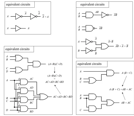
Like conventional algebra, Boolean algebra has a set of logic identities that can be used to simplify the Boolean expressions and thus make circuits more compact. These identities go by such names as the commutative law of addition, associate law of addition, distributive law, etc. Instead of worrying about what the various identities are called, simply make reference to the list of identities provided below and to the left. Most of these identities are self-explanatory, although a few are not so obvious, as you will see in a minute. The various circuits below and to the right show some of the identities in action.
LOGIC IDENTITIES 1) A+B=B+A 2) AB=BA
3) A+(B+C) =(A+B) +C 4) A(BC) =(AB)C
5) A(B+C) =AB+AC
6) (A+B)(C+D) =AC+AD+BC+BD 7) 1=0
8) 0=1 9) A0 =0 10) A1 =A 11) A+0 =A 12) A+1 =1 13) A+A=A 14) AA=A 15) A=A 16) A+A=1 17) AA=0 18) A+B=AB
19) AB=A+B 20) A+AB=A+B 21) A+AB=A+B
22) AB=AB+AB=(A+B)(AB) 23) AB=AB+AB
EXAMPLE
Let’s find the initial Boolean expression for the circuit in Fig. 12.20 and then use the logic identities to come up with a circuit that requires fewer gates.
Y = AB A
B
Y
A
B Y = AB
Y = ABC Y
B A
C
B A
Y
Y
Y = ABC A B
A B
B A
C
B A
C
Y
Y
Y
Y
Y = A+B
Y = A+B
Y = A+B+C
Y = A+B+C
A Y
A B
A B
Y
Y Y = A
Y = A B
Y = A B
Boolean expressions for the logic gates
A
A
A = A A
A A
equivalent circuits
A
B C
A (B + C)
A B
C
AB + AC A (B + C) =AB + AC
equivalent circuits
A B
C D
(A+B)(C+D)
A
C
D C
B D A A
B
C B
D AC
AD
BC
BD
AC+AD+BC+BD (A+B)(C+D)
= AC+AD+BC+BD
equivalent circuits
A
B AB
AB = A + B A
B
A
B
A+B A
B
AB
AB
equivalent circuits
[image:15.612.258.539.395.638.2]FIGURE 12.18
The circuit shown here is expressed by the following Boolean expression:
out=(A +B)B+B+BC
This expression can be simplified by using Identity 5:
(A +B)B=AB+BB
This makes
out =AB+BB+B+BC
Using Identities 17 (BB=0) and 11 (B+0 =B), you get out =AB+0 +B+BC =AB+BC
Factoring a Bfrom the preceding term gives
out =B(A+1) +BC
Using Identities 12 (A+1 =1) and 10, you get out =B(1) +BC =B+BC
Finally, using Identity 21, you get the simplified expression
out =B+C
Notice that Ais now missing.This means that the logic input at Ahas no effect on the output and therefore can omitted. From the reduction, you get the simplified circuit in the bottom part of the figure.
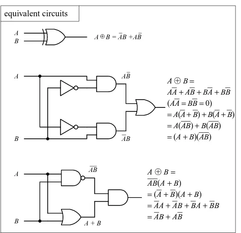
Dealing with Exclusive Gates (Identities 22 and 23)
Now let’s take a look at a couple of not so obvious logic identities I mentioned a sec-ond ago, namely, those which involve the XOR (Identity 22) and XNOR (Identity 23) gates. The leftmost section below shows equivalent circuits for the XOR gate. In the lower two equivalent circuits, Identity 22 is proved by Boolean reduction. Equivalent circuits for the XNOR gate are show in the rightmost section below. To prove Identity 23, you can simply invert Identity 22.
A
B
C
A+B
B
BC
B
C A
logic level at A has no effect on output
B+C
(A+B)B+B+BC
not used
A
B
AB
AB
A
B A
B A B = AB +AB
equivalent circuits
AB
A + B
AB=
AA+ AB+ BA+ BB (AA=BB=0)
=A(A+ B) +B(A+ B)
=A(AB) +B(AB)
=(A+ B)(AB)
A
B A B = AB + AB
A
B
AB
AB
AB+AB
B A
A B = AB +AB
AB+AB equivalent circuits
[image:16.612.73.310.497.726.2]AB= A B(A+ B) =(A+ B)(A+ B) =AA+ AB+ BA+ BB =AB+ AB
[image:16.612.356.556.502.712.2]FIGURE 12.20
De Morgan’s Theorem (Identities 18 and 19)
To simplify circuits containing NANDs and NORs, you can use an incredibly useful theorem known as De Morgan’s theorem. This theorem allows you to convert an expression having an inversion bar over two or more variables into an expression having inversion bars over single variables only. De Morgan’s theorem (Identities 18 and 19) is as follows:
A
⋅B=A+B (2 variables) ABC=A+B+C (3 or more variables) A
+B=AB A+B+C=ABC
The easiest way to prove that these identities are correct is to use the figure below, noting that the truth tables for the equivalent circuits are the same. Note the inversion bubbles present on the inputs of the corresponding leftmost gates. The inversion bub-bles mean that before inputs A and B are applied to the base gate, they are inverted (negated). In other words, the bubbles are simplified expressions for NOT gates.
Why do you use the inverted-input OR gate symbol instead of a NAND gate sym-bol? Or why would you use the inverted-input AND gate symbol instead of a NOR gate symbol? This is a choice left up to the designer—whatever choice seems most logical to use. For example, when designing a circuit, it may be easier to think about ORing or ANDing inverted inputs than to think about NANDing or NORing inputs. Similarly, it may be easier to create truth tables or work with Boolean expressions using the inverted-input gate—it is typically easier to create truth tables and Boolean expressions that do not have variables joined under a common inversion bar. Of course, when it comes time to construct the actual working circuit, you probably will want to convert to the NAND and NOR gates because they do not require additional NOT gates at their inputs.
Bubble Pushing
A shortcut method for forming equivalent logic circuits, based on De Morgan’s theo-rem, is to use what’s called bubble pushing.
A B
A B
A+B A • B
A
B AB
A
B A+B
= =
= =
=
A B A•B
0 0 1
0 1 1
1 0 1
1 1 0
A B A+ B
0 0 1
0 1 1
1 0 1
1 1 0
A B A+B
0 0 1
0 1 0
1 0 0
1 1 0
A B A•B
0 0 1
0 1 0
1 0 0
1 1 0
FIGURE 12.22
Bubble pushing involves the flowing tricks: First, change an AND gate to an OR gate or change an OR gate to an AND gate. Second, add inversion bubbles to the inputs and outputs where there were none, while removing the original bubbles. That’s it. You can prove to yourself that this works by examining the corresponding truth tables for the original gate and the bubble-pushed gate, or you can work out the Boolean expressions using De Morgan’s theorem. Figure 12.23 shows examples of bubble pushing.
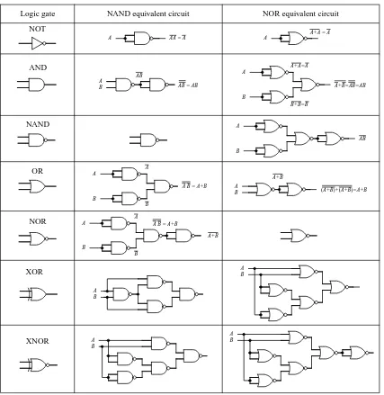
Universal Capability of NAND and NOR Gates
NAND and NOR gates are referred to as universal gates because each alone can be combined together with itself to form all other possible logic gates. The ability to cre-ate any logic gcre-ate from NAND or NOR gcre-ates is obviously a handy feature. For exam-ple, if you do not have an XOR IC handy, you can use a single multigate NAND gate (e.g., 74HC00) instead. The figure below shows how to wire NAND or NOR gates together to create equivalent circuits of the various logic gates.
A
B
A
B
A B = A+B
A+B A
B AB = AB
AB
A AA = A
A
B
A
B
A B = A+B A B
A+B
(A+B)+(A+B)=A+B A
B
AB A
A+A = A
A
B
A+A=A
B+B=B
A+B=AB=AB
NOT
XOR
XNOR
A B
A B
A B
A B
Logic gate NAND equivalent circuit NOR equivalent circuit
AND
NAND
OR
[image:18.612.74.501.286.725.2]NOR
AND-OR-INVERT Gates (AOIs)
When a Boolean expression is reduced, the equation that is left over typically will be of one of the following two forms: product-of-sums (POS) or sum-of-products (SOP). A POS expression appears as two or more ORed variables ANDed together with two or more additional ORed variables. An SOP expression appears as two or more ANDed variables ORed together with additional ANDed variables. The figure below shows two circuits that provide the same logic function (they are equivalent), but the circuit to the left is designed to yield a POS expression, while the circuit to the right is designed to yield a SOP expression.
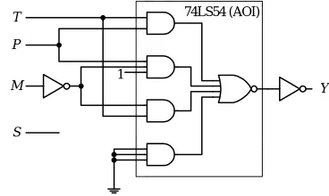
In terms of design, which circuit is best, the one that implements the POS expres-sion or the one that implements SOP expresexpres-sion? The POS design shown here would appear to be the better choice because it requires fewer gates. However, the SOP design is nice because it is easy to work with the Boolean expression. For example, which Boolean expression above (POS or SOP) would you rather use to create a truth table? The SOP expression seems the obvious choice. A more down-to-earth reason for using an SOP design has to do with the fact that special ICs called AND-OR-INVERT (AOI) gates are designed to handle SOP expressions. For example, the 74LS54 AOI IC shown below creates an inverted SOP expression at its output, via two 2-input AND gates and two 3-input AND gates NORed together. A NOT gate can be attached to the output to get rid of the inversion bar, if desired. If specific inputs are not used, they should be held high, as shown in the example circuit below and to the far left. AOI ICs come in many different configurations—check out the catalogs to see what’s available.
0
A D
0 0 0 0 0 0 0 1
0 1 0 0 0 1 0 1 0 0 1 0
1 0 1 0 1 1 0 1 1 1 0 0
0 1 0 1 0 0 1 0 1 1 0 1
1 0 1 1 1 0 1 1 0 1 1 1
0 1 0 1 1 1 1
A C
A B C D B C B D
0 0 1 0
X
0 0 1 1
0 0 0 0
0 0 0 1
0 0 0 0
0 0 0 0
0 0 0 0
0 0 0 0
1 0 1 0
1 1 1 1
0 0 0 0
0 1 0 1
1 0 0 0
1 1 0 0
0 0 0 0
0 1 0 0
1 1 0 1 0 0 0 0 1 1 0 1 1 1 0 1 Table made using SOP expression
(it's easier than POS)
A B
C D
A C
B C B D A
D Logic circuit for POS expression
X X
X = AC + AD + BC +BD X = ( A + B )( C + D )
Logic circuit for SOP expression
A
1 1 1
D C B
1 1 1
X = AB + CD X
Y
Y= AB + CD
unused inputs are held HIGH
A
G F E D C B
I H
J
X = AB + CDE + FG + HJK Y = AB + CDE + FG + HJK
X
Y
1 2 3 4 5 6 7
14 13 12 11 10 9 8 GND
+VCC
74LS54
AOI GATE
FIGURE 12.25
12.2.5
Keeping Circuits Simple (Karnaugh Maps)
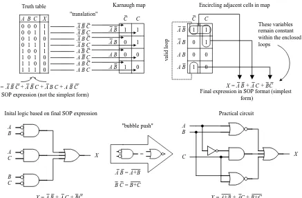
We have just seen how using the logic identities can simplify a Boolean expression. This is important because it reduces the number of gates needed to construct the logic circuit. However, as I am sure you will agree, having to work out Boolean problems in longhand is not easy. It takes time and ingenuity. Now, a simple way to avoid the unpleasant task of using your ingenuity is to get a computer program that accepts a truth table or Boolean expression and then provides you with the simplest expression and perhaps even the circuit schematic. However, let’s assume that you do not have such a program to help you out. Are you stuck with the Boolean longhand approach? No. What you do is use a technique referred to as Karnaugh mapping. With this tech-nique, you take a given truth table (or Boolean expression that can be converted into a truth table), convert it into a Karnaugh map, apply some simple graphic rules, and come up with the simplest (most of the time) possible Boolean expression for your final circuit. Karnaugh mapping works best for circuits with three to four inputs— below this, things usually do not require much thought anyway; beyond four inputs, things get quite tricky. Here’s a basic outline showing how to apply Karnaugh map-ping to a three-input system:
1. First, select a desired truth table. Let’s choose the one shown in Fig. 12.27. (If you only have a Boolean expression, transform it into an SOP expression and use the SOP expression to create the truth table—refer to Fig. 12.26 to figure out how this is done.)
2. Next, translate the truth table into a Karnaugh map. A Karnaugh map is similar to a truth table but has its variables represented along two axes. Translating the truth
C C
A B
A B
A B
A B
1 1
1
1 0 0 0 1
0 0 1 1 0 1 0 0 0 1 1 1 1 0 0 1 1 0 1 0 1 1 0 0 1 1 1 0 A B C X Truth table
X = A B + A C + BC C C
A B
A B
A B
A B
1 1
1
1
These variables remain constant within the enclosed loops
v
alid loop
Karnaugh map Encircling adjacent cells in map
Final expression in SOP format (simplest form)
0
0 0
0
Inital SOP expression (not the simplest form) A B C A B C
A B C A B C A B C
A B C A B C A B C "translation"
A B C + A B C + A B C + A B C X =
0
0 0
0
A B
A C
B C
X
B A
C X
= "bubble push"
X = A B + A C + BC X = A+B + AC + B+C
Practical circuit
A B = A+B
[image:20.612.90.527.433.720.2]B C = B+C Inital logic based on final SOP expression
table into a Karnaugh map reduces the number of 1s and 0s needed to present the information. Figure 12.27 shows how the translation is carried out.
3. After you create the Karnaugh map, you proceed to encircle adjacent cells of 1s into groups of 2, 4, or 8. The more groups you can encircle, the simpler the final equation will be. In other words, take all possible loops.
4. Now, identify the variables that remain constant within each loop, and write out an SOP equation by ORing these variables together. Here, constant means that a variable and its inverse are not present together within the loop. For example, the top horizontal loop in Fig. 12.27 yields AB(the first term in the SOP expression), since A’s and B’s inverses (A and B) are not present. However, the C variable is omitted from this term because C and Care both present.
5. The SOP expression you end up with is the simplest possible expression. With it you can create your logic circuit. You may have to apply some bubble pushing to make the final circuit practical, as shown in the figure below.
To apply Karnaugh mapping to four-input circuits, you apply the same basic steps used in the three-input scheme. However, now you use must use a 4 ×4 Karnaugh map to hold all the necessary information. Here is an example of how a four-input truth table (or unsimplified four-variable SOP expression) can be mapped and con-verted into a simplified SOP expression that can be used to create the final logic circuit:
Unsimplified SOP expression:
A
⋅B⋅C⋅D +A⋅B⋅C ⋅D +A⋅B ⋅C⋅D +A⋅B ⋅C ⋅D
+A⋅B ⋅C ⋅D +A⋅B⋅C⋅D +A⋅B⋅C ⋅D +A⋅B ⋅C⋅D +A⋅B ⋅C ⋅D =Y Simplified SOP expression and circuit
Here’s an example that uses an AOI IC to implement the final SOP expression after mapping. I’ve thrown in variables other than the traditional A, B, C, and D just to let you know you are not limited to them alone. The choice of variables is up to you and usually depends on the application.
inputs out
A B C D Y
0 0 0 0 0
0 0 0 1 1
0 0 1 0 0
0 0 1 1 1
0 1 0 0 0
0 1 0 1 1
0 1 1 0 1
0 1 1 1 1
1 0 0 0 0
1 0 0 1 1
1 0 1 0 0
1 0 1 1 1
1 1 0 0 0
1 1 0 1 1
1 1 1 0 0
1 1 1 1 1
A B
A B
A B
A B
C D C D C D C D
1 1
1 1
1 1
1 1
1
D + A B C = Y These variables remain constant within the enclosed loops
A B C
D Y
T P
T P
T P
T P
M S M S M S M S
1 1
1 1 1
1 1
1 T P + P M + T M = Y
These variables remain constant within the enclosed loops
Y
74LS54 (AOI)
T
P
M
S
1
[image:21.612.348.532.616.726.2]FIGURE 12.28
Other Looping Configurations
Here are examples of other looping arrangements used with 4 ×4 Karnaugh maps:
12.3
Combinational Devices
Now that you know a little something about how to use logic gates to enact functions represented within truth tables and Boolean expressions, it is time to take a look at some common functions that are used in the real world of digital electronics. As you will see, these functions are usually carried out by an IC that contains all the neces-sary logic.
A word on IC part numbers before I begin. As with the logic gate ICs, the combi-national ICs that follow will be of either the 4000 or 7400 series. It is important to note that an original TTL IC, like the 74138, is essentially the same device (same pinouts and function—usually, but not always) as its newer counterparts, the 74F138, 74HC128 (CMOS), 74LS138, etc. The practical difference resides in the overall perfor-mance of the device (speed, power dissipation, voltage level rating, etc.). I will get into these gory details in a bit.
12.3.1
Multiplexers (Data Selectors) and Bilateral Switches
Multiplexers or data selectors act as digitally controlled switches. (The term data selec-tor appears to be the accepted term when the device is designed to act like an SPDT switch, while the term multiplexer is used when the throw count of the “switch” exceeds two, e.g., SP8T. I will stick with this convention, although others may not.) A simple 1-of-2 data selector built from logic gates is shown in Fig. 12.32. The data select input of this circuit acts to control which input (A or B) gets passed to the out-put: When data select is high, input A passes while B is blocked. When data select is low, input B is passed while B is blocked. To understand how this circuit works, think of the AND gates as enable gates.
A B
1 1
1 1
1
A B
A B
A B
C D C D C D C D
1
A B
1 1
1 1 1
1
A B
A B
A B
C D C D C D C D
A B 1
1 1
1
1
1 1 1
1 1
A B
A B
A B
C D C D C D C D
A B 1
1 1
1 1
1 1
1 1
1
A B
A B
A B
C D C D C D C D
Y = BD + BC Y = ABD + ABC + CD Y = B + A D Y = A + B D
Same basic device, different technology
74138
3-line to 8-line decoder/ demultiplexer
(7400 series)
74F138 74HC138 74HCT138
74LS138 74ALS138
etc. 4063
4-bit magnitude comparitor
(4000 series)
FIGURE 12.30
There are a number of different types of data selectors that come in IC form. For example, the 74LS157 quad 1-of-2 data selector IC, shown in Fig. 12.32, acts like an electrically controlled quad SPDT switch (or if you like, a 4PDT switch). When its select input is set high (1), inputs A1, A2, A3, and A4are allowed to pass to outputs Q1, Q2, Q3, and Q4. When its select input is low (0), inputs B1, B2, B3, and B4are allowed to
pass to outputs Q1, Q2, Q3, and Q4. Either of these two conditions, however, ultimately
depends on the state of the enable input. When the enable input is low, all data input signals are allowed to pass to the output; however, if the enable is high, the signals are not allowed to pass. This type of enable control is referred to as active-low enable, since the active function (passing the data to the output) occurs only with a low-level input voltage. The active-low input is denoted with a bubble (inversion bubble), while the outer label of the active-low input is represented with a line over it. Some-times people omit the bubble and place a bar over the inner label. Both conventions are used commonly.
Figure 12.33 shows a 4-line-to-1-line multiplexer built with logic gates. This cir-cuit resembles the 2-of-1 data selector shown in Fig. 12.32 but requires an additional select input to provide four address combinations.
A
B
data select
out
Data select input: LOW(0) = selects A HIGH(1) = selects B Simple 1-of-2 data selector
2
3
5
11
10
14 6
13 A1
B1
A2
B2
A3
A4
B3
B4
Select
Select: HIGH (1) = A inputs selected LOW (0) = B inputs selected Enable: HIGH (1) = outputs disabled LOW (0) = outpus enabled Enable
4
7
9
12
16 8
15 1
+VCC GND
74LS157
Q1
Q2
Q3
Q4
74LS157 quad 1-of-2 data selector 4066 quad bilateral switch
16 15 14 13 12 11 10 1 2 3 4 5 6 7
74LS157
9 8
A B C D
13 5 6 12
10 11
8 9
3 4
1 2
4066
Control logic 0 = switch OFF 1 = switch ON VDD
14 VSS
14 13 12 11 10 9 8 1 2 3 4 5 6 7
4066
Digital control
A
B
out
data select
Switch analogy
Enable Select
A
S0
B
C
D
S1
1
2
3
4
C
0
1 1
0 select inputs
output
S1 S0
0 0 0 1 1 0 1 1
transmitted input
A B C D
4-line to 1-line multiplexer
VCC = pin 16 GND = pin 8
8-line to 1-line multiplexer
74HC151
I7
data
inputs data
select 6
I6 I5 I4 I3 I2 I1 I0
S0 Y 5
11 10 9 4
3 2 1 15 14 13 12
Y
S1
S2
7 E
output output active-LOW
enable input S1 S2 S3
0 0 0 0 0 1 0 1 0 0 1 1 1 0 0 1 0 1 1 1 0 1 1 1
data out (Y )
I0 I1 I2 I3 I4 I5 I6
I7
When enable (E ) is set HIGH (1), all inputs are disabled— output (Y ) is forced LOW (0) regardless of all other inputs.
FIGURE 12.32