This is a repository copy of
Effect of component variations on the gate fidelity in linear
optical networks
.
White Rose Research Online URL for this paper:
http://eprints.whiterose.ac.uk/107982/
Version: Accepted Version
Article:
Crickmore, J., Frazer, J., Shaw, S. et al. (1 more author) (2016) Effect of component
variations on the gate fidelity in linear optical networks. Physical Review A, 94 (2). 022326.
ISSN 2469-9926
https://doi.org/10.1103/PhysRevA.94.022326
[email protected] https://eprints.whiterose.ac.uk/
Reuse
Unless indicated otherwise, fulltext items are protected by copyright with all rights reserved. The copyright exception in section 29 of the Copyright, Designs and Patents Act 1988 allows the making of a single copy solely for the purpose of non-commercial research or private study within the limits of fair dealing. The publisher or other rights-holder may allow further reproduction and re-use of this version - refer to the White Rose Research Online record for this item. Where records identify the publisher as the copyright holder, users can verify any specific terms of use on the publisher’s website.
Takedown
If you consider content in White Rose Research Online to be in breach of UK law, please notify us by
Jonathan Crickmore,1, 2 Jonathan Frazer,1 Scott Shaw,1 and Pieter Kok1,∗
1
Department of Physics & Astronomy, University of Sheffield, Sheffield S3 7RH, United Kingdom 2
Department of Physics, Heriot-Watt University, Edinburgh, United Kingdom
(Dated: August 2, 2016)
We investigate the effect of variations in beam splitter transmissions and path length differences in the nonlinear sign gate that is used for linear optical quantum computing. We identify two im-plementations of the gate, and show that the sensitivity to variations in their components differs significantly between them. Therefore, circuits that require a precision implementation will generally benefit from additional circuit analysis of component variations to identify the most practical imple-mentation. We suggest possible routes to efficient circuit analysis in terms of quantum parameter estimation.
I. INTRODUCTION
Optical networks are important for a wide variety of ap-plications, from conventional optical routers and clas-sical optical computing [1] to quantum communication networks, linear optical quantum computing and optical metrology [2–4]. The physical system that underpins all of these networks is the multi-mode interferometer. It is a collection of passive optical elements such as beam splitters, phase shifters and polarisers, as well as active elements such as optical squeezers, photodetectors and switches. These networks can be implemented in bulk optics, fibre optics, or on chip. The typical applications such as optical quantum computing, quantum imaging and quantum metrology all require an extremely high precision in the optical elements. However, in any prac-tical implementation there will be significant variations in the interferometer elements (sometimes exceeding 10% of the specified value). Depending on the application, such variations may be critically detrimental to the oper-ation of the interferometer. Furthermore, the varioper-ations in some elements will have a much greater effect on the functionality of the interferometer than those of others. It is therefore key to improve our understanding of ele-ment sensitivity of optical circuits.
The susceptibility of optical circuits to variations in their components has been studied before, particularly in the context of optical quantum information process-ing. The effect of imperfect detectors in linear optical quantum computing was studied by Glancy et al. [5], and beam splitter variations as a source of statistical er-rors in linear optical gates were considered by Ralph et al. [6]. Lund et al. considered the effect of non-ideal ancilla mode creation and detection [7]. Rohde, Ralph and Nielsen studied mode mis-matching in the temporal and frequency domain, and determined the optimal wave packet shapes to reduce mode mis-matching errors [8, 9]. A general approach to systematic errors in linear opti-cal gates was provided by Rohde, Pryde, O’Brien and
∗Electronic address: [email protected]
Ralph [10, 11]. However, to the best of our knowledge nobody has studied the effect of variations in the ele-ments of optical circuits for different implementations of the same gate. We find, surprisingly, that different imple-mentations of the same gate—with similar complexity— can have dramatically different responses to variations in optical elements.
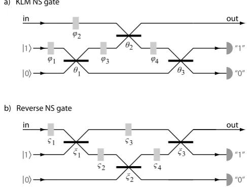
In this paper, we explore the sensitivity of the nonlin-ear sign (NS) gate used in linnonlin-ear optical quantum com-puting [2] as an example of circuit variation analysis. We consider two versions of this gate with identical circuit complexity in terms of the number of optical elements, input states and detection devices, and operating at the same success probability (see Fig. 1). We will find that the design of the gate has significant implications for the process fidelity’s sensitivity on variations in the compo-nents. This means that any optical interferometer de-sign will have to be tested against alternative dede-signs for
“1”
“0”
in out
“1”
“0”
in out
b) Reverse NS gate a) KLM NS gate
1
2
4
4 1
2
3 1
2 3 2
3
1
3 1
0
1
[image:2.595.316.560.452.637.2]0
FIG. 1: two designs for the NS gate: a) the KLM NS gate, and b) the Reverse NS gate. The two circuits have the same com-plexity in terms of components, input states and detectors, and they have the same probability of successfully applying an NS gate (psuccess=1
2
the best performance given realistic components. In Sec-tion II we present two different version of the NS gate and in Section III we study the effect of components variations. Section IV looks at the broader connection to multi-parameter estimation theory, and we conclude with a brief discussion in Section V.
II. TWO NS GATE DESIGNS
The NS gate is a key component in the original proposal by Knill, Laflamme and Milburn (KLM) for a quantum computer constructed from linear optical elements, single photon sources and photodetection [2]. The main opera-tion of the gate is to induce a nonlinear phase shiftUNS on an optical mode defined by
α|0i+β|1i+γ|2i −→UNS α|0i+β|1i −γ|2i, (1)
where|niis the state ofnphotons in the input mode and (α, β, γ) are complex amplitudes normalised to 1. The action of the NS gate on photon number states|ni with
n > 2 is not defined, and allows for additional freedom in the construction ofUNS.
The optical circuit for the original NS gate is shown in Fig. 1a. It is a simple circuit that lends itself well to analysis. However, the circuit is not unique. We can de-fine a “reverse” NS gate, shown in Fig. 1b, that achieves the same transformation on the space of zero, one and two photons, with the same probability of success. How-ever, the two implementations do differ in the way they respond to variations in the transmission coefficients on the beam splitters and path length deviations. In this pa-per we analyse the difference in pa-performance under these systematic errors of the two incarnations of the NS gate. We will refer to the original gate in Fig. 1a as the KLM NS gate, and to Fig. 1b as the Reverse NS gate.
The NS gate isnonlinear in the sense that no combina-tion of linear optical elements can implement the trans-formation in Eq. (1). The gate is induced by interfer-ence with ancilla photons in additional modes, followed by post-selection on a particular measurement outcome in the ancilla modes. This implies that the NS gate is successfully implemented with a probability smaller than one. The traditional implementation employs a single an-cilla photon and two extra optical modes [2]. The max-imum success probability of any NS gate is psuccess= 14 [12, 13], which is achieved by both implementations in Fig. 1.
Next, we establish our conventions in describing the NS gates. We define the action of a beam splitter as a matrix transformationUBSon the mode operatorsˆa1and ˆ
a2 of the two input modesa1 anda2, such that
UBSˆa1UBS† = cosθˆa1+ sinθˆa2,
UBSˆa2UBS† =−sinθˆa1+ cosθˆa2, (2)
and the mode operators are defined by the usual commu-tation relations
h ˆ aj,ˆa†k
i
=δjk, (3)
withδjk the Kronecker symbol. All other commutators are zero. The KLM NS gate in Fig. 1a has beam splitter angles
θ1= arccosη1, θ2= arccosη2, θ3=−θ1, (4)
where
η1= 1
4−2√2 and η2= 3−2
√
2. (5)
The phasesϕj in Fig. 1a are all zero [2]. We determine the beam splitter angles for the Reverse NS gate by re-quiring that the success probability of the ideal gate is again one quarter, and that the ancilla state and detec-tion signature is the same as the KLM NS gate. Since we are primarily interested in finding an alternative gate and at this point do not wish to generate a complete family of NS gates, this construction suffices. We con-struct the mode transformations from Eq. (2) and collect the terms that have a single creation operatorˆa†2 and no mode operators ˆa†3, corresponding to the post-selection on a detected photon in mode a2 and no detected pho-tons in modea3. We then obtain coefficientsc0, c1, and c2for the zero, one, and two-photon terms in the output state, respectively. Solving forc0=c1=−c2, we obtain
ξ1= arctanχ1, ξ2=π+ arctanχ2, ξ3=−ξ1, (6)
where
χ1= 4 √
8 and χ2=
p
16√2−13
7 , (7)
with all phasesζj in Fig. 1b equal to zero. Post-selection is implemented by projecting the three-mode output state onto the state|1,0i23, which has exactly one pho-ton in mode 2, and zero phopho-tons in mode 3. For these values, the coefficients|ck| = 12, yielding an overall suc-cess probability of a quarter, independent of the input state in mode a1. In the next section we consider im-perfections in the beam splitter transmission coefficients and the path lengths in the interferometer.
III. IMPERFECT COMPONENTS
and five path lengths. To this end we use the gate fi-delity as a figure of merit [14, 15]. We find that given a specified target gate fidelity, the tolerances of the optical components vary significantly.
Let E(ρ) denote a trace preserving quantum process on a density operatorρ. We define the gate fidelity ofE relative to an ideal (unitary) gateU as the quantity
F(E, U) = Z
dψhψ|U†E(ψ)U|ψi, (8)
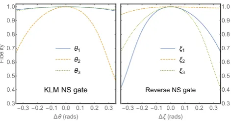
where dψis the uniform (Haar) measure over the quan-tum state space [15]. Unfortunately, the NS gate is a non-trace-preserving quantum process, since the probability of success for the gate is less than one. Moreover, the success probability of the gate changes significantly with variations in the optical components. The probabilities of finding the detector signature that heralds success for the two NS gates as a function of variations in the beam splitter angles are shown in Fig. 2. While the theoretical maximum success probability of the ideal NS gate is one quarter, larger probabilities of finding the right detector outcomes are possible when the beam splitter coefficients change and the implemented gate deviates significantly from the ideal NS gate. We note that the curves for the first and third beam splitters are mirror images of each other in both the KLM and Reverse NS gate. This is explained by the time-reversal symmetric nature of the gates, keeping in mind that time-reversed detectors are sources, and vice versa.
The variation in success probability means that we can-not use Eq. (8) in a straightforward manner. The process E must be normalised, but this means that Eq. (8) can no longer be evaluated analytically for the NS gates. In-stead, we average the gate fidelity over 10 000 random uniformly sampled input states for each value of gate component variations. Since our input state consists of a linear superposition of the first three Fock states (and ignoring a global phase), the state space is given by the unit sphere in a three-dimensional complex Hilbert space {ψ∈C3: kψk= 1}, whereCis the complex plane and k·k is the usual complex vector norm. Any state |ψi in C3 can be obtained by applying a suitable matrix U to an initial state |ψ0i, and finding a uniform distribution over the state space reduces to finding a uniform distri-bution over the set of unitary matrices U acting onC3 with respect to the Haar measure. This is accomplished using the complex normal distribution onC3 [16].
In the remainder of this section, we study the effect of beam splitter variations and path length differences individually, and calculate the minimum, maximum and mean gate fidelity for a distribution of variations across the circuit.
A. Imperfect beam splitters
The gate fidelities for the KLM and Reverse NS gate with imperfect beam splitters are shown in Fig. 3. The
KLM NS gate
θ1 θ2 θ3
0.0 0.1 0.2 0.3 -0.1
-0.2 -0.3 0.15 0.20 0.25 0.30
Δθ(rads)
S
u
cce
ss
P
ro
b
a
b
ili
ty
Reverse NS gate
ξ1 ξ2 ξ3
0.0 0.1 0.2 0.3 -0.1
-0.2 -0.3 0.15 0.20 0.25 0.30
Δξ(rads)
S
u
cce
ss
P
ro
b
a
b
ili
ty
FIG. 2: (Color online) The probability of a detector signature that heralds the success of the NS gates for varying beam splitter transmission coefficients and equal amplitudes α = β=γ = 1/√3. In the top graph,∆θj is the variation away from the ideal value θj in the KLM NS gate, while in the bottom graph∆ξj is the variation away from the ideal value ξjin the Reverse NS gate. The black line indicates the ideal success probability of one quarter. Success probabilities larger that 0.25 are allowed, and indicate a significant departure from the ideal NS gate.
KLM NS gate is particularly sensitive to variations in the second beam splitter, which is the one that directly interacts with the signal mode. The gate is significantly less sensitive to variations in the two other beam splitters. For example, at a fixed gate fidelity of F = 0.999, the tolerance in the first and third beam splitters, (∆θ1 and ∆θ3, respectively) is more than three times larger than ∆θ2. The curves for the first and third beam splitters are again mirror images of each other, as expected. The Reverse NS gate shows a similar range of sensitivities to beam splitter variations. Again, the two beam splitters in the direct signal path have the greatest effect on the gate fidelity, and the shape of these curves are very similar to the∆θ2 curve for the KLM NS gate. Again, we have mirror symmetry for the first and third beam splitters.
[image:4.595.355.523.59.293.2]4
KLM NS gate
θ1
θ2
θ3
0.0 0.1 0.2 0.3
-0.1
-0.2
-0.3 0.3 0.4 0.5 0.6 0.7 0.8 0.9 1.0
Δθ(rads)
F
id
e
lit
y
Reverse NS gate
ξ1
ξ2
ξ3
0.0 0.1 0.2 0.3 -0.1
-0.2
-0.3 0.3
0.4 0.5 0.6 0.7 0.8 0.9 1.0
Δξ(rads)
FIG. 3: (Color online) The gate fidelity of the KLM and Re-verse NS gate for variations ∆θ and ∆ξ in the three beam splitters, respectively. The Reverse NS gate is most sensitive to the first and third beam splitter, while the KLM NS gate is sensitive only to the second.
to be corrected in this way, the better. Generally, there will be room to optimise the circuit design based on the tolerances of the circuit on the variations in its elements. In practice, variations in beam splitters can be quite large in bulk optics (on the order of 10%).
B. Variations in path lengths
A similar analysis can be performed for the various path length differences in the circuit. The KLM NS gate is completely insensitive to path length variations encoded in the phases ϕ1 and ϕ2, as expected. Similarly, the Reverse NS gate is insensitive to variations in ζ1 (see Fig. 4). For the remaining phases there is a marked dif-ference in the two gates. The KLM NS gate loses only about a percent in fidelity when the path lengths associ-ated with ϕ3 and ϕ4 varies by half a wavelength, while the Reverse gate sees a significant drop in average gate fidelity. Compared to the beam splitter variations we can say that the KLM NS gate is effectively insensitive to path length differences, while the Reverse NS gate is very sensitive to path length differences. This is another reason to strongly prefer the KLM NS gate over the Re-verse NS gate, and underlines the importance of circuit analysis for component variations.
C. Compound variations
In addition to individual errors in components, we may consider compound errors in all beam splitters and path lengths. This describes the more realistic behaviour where all components are subject to small variations. We define an error vectorδwith eight components (three for
the beam splitters and five for the path lengths) and mag-nitude |δ|. For a given total error r distributed among
the components, all possible error configurations are de-scribed by a 7-sphere of radius|δ|. We randomly sample
KLM NS gate
φ1
φ2
φ3
φ4
0.0 0.3 0.6 0.9 -0.3
-0.6 -0.9 0.990 0.992 0.994 0.996 0.998 1.000
Δφ(rads)
F
id
e
lit
y
Reverse NS gate
ζ1
ζ2
ζ3
ζ4
0.0 0.3 0.6 0.9
-0.3
-0.6
-0.9 0.5
0.6 0.7 0.8 0.9 1.0
Δζ(rads)
FIG. 4: (Color online) The gate fidelity of the KLM and Re-verse NS gate for variations∆ϕjand∆ζkin the four relevant path lengths, respectively. The KLM NS gate is again far less sensitive to path length variations than the Reverse NS gate.
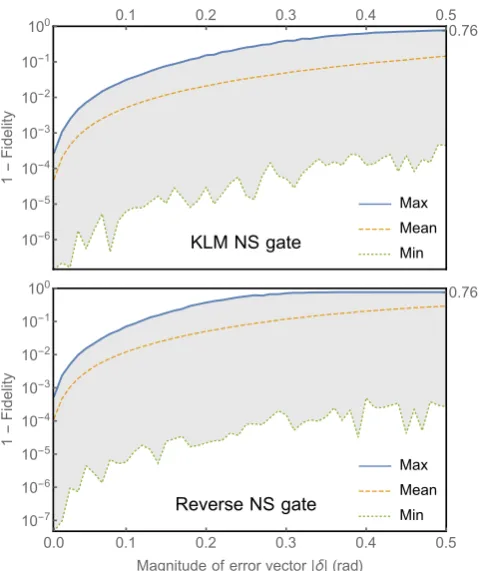
this error space and calculate the gate fidelity. The re-sults are shown in Fig. 5.
For each value of |δ| we generate 50 000 random
vec-tors δ. The gate fidelity for each δ is then calculated
again using 10 000 random input states into the NS gate. In Fig. 5 we plot the minimum, maximum and mean gate infidelity1−F as a function of |δ|. The maximum gate
infidelity is the worst case scenario for a given |δ|. It
reaches a maximum of approximately 0.76 with increas-ing |δ| for both the KLM and Reverse NS gate. This
value represents the limit where the circuit is so badly constructed that it no longer outperforms a randomly constructed circuit, and we call this the randomisation limit. The gate infidelity of the Reverse NS gate reaches this value much faster than the KLM NS gate, which is consistent with our earlier observation that the Reverse NS gate is more sensitive to variations in the two in-line beam splitters, compared to the KLM NS gate that is sensitive to variations in the single in-line beam splitter. In both cases the effect of path length variations is much less important than the beam splitter variations.
The minimum gate infidelity exhibits strong statistical fluctuations (the green lines in Fig. 5). This is due to the long tail in the fidelity distribution for given |δ|. Only
relatively few circuit configurationsδwill give a high gate
fidelity, and the finite number of samples (50 000) is un-likely to hit upon the true minimum gate infidelity. This line is therefore more accurately characterised as a lower bound on the maximum gate fidelity (or, equivalently, an upper bound on the minimum gate infidelity).
[image:5.595.60.296.56.180.2] [image:5.595.319.562.57.182.2]KLM NS gate
Max
Mean
Min
10-6 10-5
10-4
10-3
10-2
10-1
100 0.1 0.2 0.3 0.4 0.5
0.76
1
-F
id
e
lit
y
Reverse NS gate
Max
Mean
Min
0.0 0.1 0.2 0.3 0.4 0.5
10-7 10-6 10-5 10-4 10-3 10-2 10-1 100
0.76
Magnitude of error vector|δ| (rad)
1
-F
id
e
lit
y
FIG. 5: (Color online) Minimum (dotted green), maximum (solid blue), and mean (dashed orange) gate infidelity as a function of the compound error |δ| for the KLM (top) and Reverse (bottom) NS gates. The minimum gate fidelity ex-hibits strong statistical fluctuations due to the relatively long tail in the distribution of gate fidelities for a given|δ|. Both circuits reach the same randomisation limit of 0.76.
IV. QUANTUM ESTIMATION OF CIRCUIT
COMPONENTS
One potentially fruitful approach towards analysing the effect of component variations on the gate fidelity in linear optical networks is to use the theory of multi-parameter quantum estimation. When we consider the components of the multi-mode interferometer, the varia-tions away from the ideal designed value become a vector of random variables δ in a parameter estimation
prob-lem. We can then use techniques from quantum metrol-ogy [20], information geometry [21], and the theory of the dynamical evolution of quantum states [22] to shed light on the sensitivity of an interferometer on its elements.
The quantum Fisher information (QFI) is a metric in the state space that is parametrised by the random vari-ables δ. It is a special case of the Bures metric [23].
Intuitively, the quantum Fisher informationIQ(δ)is the
amount of information about δ that is contained in the
state |ψi. However, for our purposes it is sufficient to note that a large QFI means that we can detect small variations inδ. Therefore,IQ(δ)is also a metric for the
sensitivity of|ψionδ.
Let a unitary transformation of an optical circuit be
U
U
Uc
1 2
[image:6.595.57.297.49.335.2]optimal conditional state
FIG. 6: The optimal conditional state |Ψopt
c i is taken just before the componentcof interest (dashed line), and it is the state that maximises the quantum Fisher information (eval-uated by the variance of the generator ofUc with respect to |Ψopt
c i), while still being capable of triggering the detector array in the required way.
denoted byU, and deviations in the characteristics of a component c (such as a beam splitter or phase shifter) are generated byGc. The unitary transformation corre-sponding to an inaccurate component is then
e
Uc(δc) = exp(−iGcδc)Ucexp(iGcδc), (9)
where δc is a component of the vector δ. The QFI for δc is bounded by the variance(∆Gc)2 ofGcwith respect to the optical quantum state|Ψci immediately prior to the componentc [24]. By studying(∆Gc)2 with respect to a variety of quantum states |Ψci (average, best and worst case scenario) we can estimate the effect of varia-tions of that component on the total gate. Post-selection on a particular detection signature (as in the case of the NS gate) will typically exclude certain states|Ψci, and the most informative average QFI will no longer be due to a uniform distribution of |Ψci in the quantum state space. Instead, the set of |Ψci that are to be averaged over should be constructed from a uniform distribution of input states over all the non-ancilla input modes, ten-sored with the ancilla input states and transformed to the state just before the componentc.
The above procedure still requires averaging over a large number of states. To circumvent this lengthy pro-cess, we need a way to determine the optimal conditional state that maximises the QFI as evaluated by(∆Gc)2, while still being capable of triggering the detectors ac-cording to the required signature (see Fig. 6). The vari-ance(∆Gc)2must be evaluated with respect to this opti-mal state|Ψopt
c i. Again, this may be a computationally difficult problem.
Finally, we can calculate the weighted averageWcover the variance(∆Gc)2
Ψas a measure of the sensitivity of a component to variations:
Wc= Z
dΨpΨ(∆Gc)2Ψ, (10)
[image:6.595.356.523.51.148.2]6
entering component c. For the NS gate this is a three-mode state. We also explicitly included the subscript on
(∆Gc)2
Ψ to remind ourselves that the variance depends on the input state. Which of these approaches is most suitable likely depends on the specifics of the optical cir-cuit under consideration, and the exact relation between circuit analysis and quantum parameter estimation will be the subject of future studies.
V. DISCUSSION AND CONCLUSIONS
We have shown that the construction of optical networks that implement a given unitary transformation is gener-ally not unique, and that variations in the components of the network can have dramatically different effects on the network (gate) fidelity. Moreover, different net-work topologies for the same transformation may place very different precision requirements on the components, and any practical implementation should involve a cir-cuit analysis on how to best implement the optical
net-work. For small networks, a simple numerical calculation of the average gate fidelity may be tractable, but larger networks require more sophisticated methods. One such method is the quantum Fisher information, which can be calculated efficiently for optical components by consider-ing the variance of the generator of translations.
Our findings prompt a number of important questions for future research into the practical construction of op-tical networks: (i) Why do some elements in a network require much more precise fabrication than others? (ii) How can we design optical networks that minimise the number of sensitive elements? (iii) How can we determine the component characteristicsin situ, after the network has been fabricated? These questions will be studied fur-ther in future work.
Acknowledgements
PK thanks Mercedes Gimeno-Segovia for stimulating dis-cussions on alternative implementations of the NS gate.
[1] H. J. Caulfield and S. Dolev, Nature Photon. 4, 261 (2010).
[2] E. Knill, R. Laflamme, and G. J. Milburn, Nature409, 46 (2001).
[3] P. Kok, K. Nemoto, T. C. Ralph, J. P. Dowling, and G. J. Milburn, Rev. Mod. Phys. 79, 135 (2007).
[4] P. Kok and B. W. Lovett,Introduction to Optical Quan-tum Information Processing (Cambridge, 2010).
[5] S. Glancy, J. M. LoSecco, H. M. Vasconcelos, and C. E. Tanner, Phys. Rev. A65, 062317 (2002).
[6] T. C. Ralph, N. K. Langford, T. B. Bell, and A. G. White, Phys. Rev. A65, 062324 (2002).
[7] A. P. Lund, T. B. Bell, and T. C. Ralph, Phys. Rev. A
68, 022313 (2003).
[8] P. P. Rohde and T. C. Ralph, Phys. Rev. A71, 032320 (2005).
[9] P. P. Rohde, T. C. Ralph, and M. A. Nielsen, Phys. Rev. A72, 052332 (2005).
[10] P. P. Rohde, G. J. Pryde, J. L. O’Brien, and T. C. Ralph, Phys. Rev. A72, 032306 (2005).
[11] P. P. Rohde and T. C. Ralph, Phys. Rev. A73, 062312 (2006).
[12] S. Scheel and N. Lutkenhaus, New J. Phys.6, 51 (2004). [13] J. Eisert, Phys. Rev. Lett.95, 040502 (2005).
[14] M. D. Bowdrey, D. Oi, A. J. Short, K. Banaszek, and J. A. Jones, Phys. Lett. A294, 258 (2002).
[15] M. A. Nielsen, Phys. Rev. A303, 249 (2002). [16] I. Nechita, Ann. H. Poincaré8, 1521 (2007).
[17] M. Li, W. H. P. Pernice, and H. X. Tang, Nature Photon.
3, 464 (2009).
[18] Q. Xu, L. Chen, M. G. Wood, P. Sun, and R. M. Reano, Nature Commun.5, 346 (2014).
[19] J. C. F. Matthews, A. Politi, A. Stefanov, and J. L. O’Brien, Nature Photon.3, 346 (2009).
[20] V. Giovannetti, S. Lloyd, and L. Maccone, Nature Phot.
5, 222 (2011).
[21] S. Amari and H. Nagaoka,Methods in Information Ge-ometry (Oxford, 1993).
[22] P. J. Jones and P. Kok, Phys. Rev. A82, 022107 (2010). [23] C. W. Helstrom, Phys. Lett. A25, 101 (1967).