Abstract — This review takes a look at the historical development of the dielectric planar waveguide laser leading to key state-of-the-art technologies which fall within this broad subject area. Discussed herein are many of the advantages offered by the waveguide geometry such as; high optical-gain and thus low threshold-power requirements, suitability for quasi-three-level laser transitions, integration with functional devices on single substrates, guided spatial-mode control, and its considerable immunity to thermal effects and external environmental conditions. A detailed snapshot is made of many active host media for which there has been reported laser action in the planar waveguide geometry, covering many of the major rare-earth-ion transitions. Several fabrication techniques are highlighted and appraised for their applicability to different host media, touching on their benefits and drawbacks. Challenges and future prospects for these lasers are considered.
Index Terms— dielectric waveguides, lasers, optical planar waveguides
I. INTRODUCTION
Guided-wave lasers were amongst the first lasers demonstrated, their operation reported as early as 1961 [1]. The primary motivation at the time, as it is today, was to reduce the cavity mode-volume, through optical confinement in the active host. Thus exploiting the resulting high optical-gain [2] and low threshold-powers, and simultaneously circumventing the then difficult process of fabricating large optical-quality laser materials. The ease with which high inversion densities can be achieved in a waveguide is extremely beneficial for amplifiers and laser materials that suffer re-absorption at the emission wavelength, such as (quasi) three-level transitions, or similarly ones with weak stimulated emission cross-section [3]. Today, there are a large number of fabrication techniques available that offer an extensive range of active thin-film materials from which to choose [4-7]. In addition, the laser cavity may be entirely contained within a compact planar substrate, allowing integration with other “on-chip” optical applications, or simply used as stand-alone sources that are insensitive to
Manuscript received November 10, 2006.
J. I. Mackenzie is with the Optoelectronic Research Centre, University of Southampton, Southampton, Hampshire, SO17 1BJ, UK (phone: +44-23-80592693; fax: +44-23-80593142; e-mail: [email protected]).
external environmental conditions. One further benefit derived from the geometry of the waveguide is a high degree of thermal immunity due to its large aspect-ratio and thus large cooling-surface-area to volume ratio [8]. Therefore, the temperature rise in the active layer, dependent upon the density of the heat deposited during the pumping cycle and the thermal resistance between it and the heat sink, can be maintained at very modest levels. These are ideal for temperature sensitive quasi-three-level systems and advantageous for high-average-power devices.
The remainder of this review will concentrate on the progress of dielectric planar-waveguide lasers, for which, in recent years, there has been significant progress made by many research groups around the world. To set the scene for the interest shown for these lasers, Section II takes a closer look at the historical trends, the advantages of this laser-architecture, and the developments that brought us to the current state of the art. Following, in Section III, there is a brief discussion of key fabrication techniques; future challenges for planar waveguide lasers are discussed in Section IV; and concluding remarks are made in Section V.
II. HISTORICAL CONTEXT A. The early years
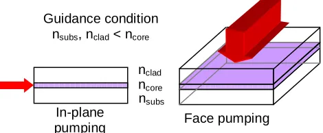
A planar waveguide consists of thin layers of optically transparent media, with a guiding core of higher refractive index (ncore) than the adjacent substrate and cladding layers
(nsubs, nclad), as illustrated in Fig. 1., forming a structure with
a “rectangular” geometry. The materials used to make active waveguides can be either dielectric or semi-conducting, corresponding to two subsets of the more generic term planar-waveguide laser (PWL). Further optical confinement in the
Dielectric Solid-State Planar Waveguide Lasers:
a Review
Jacob I. Mackenzie (Invited Paper)
nclad
nsubs
ncore
Guidance condition nsubs, nclad < ncore
Face pumping In-plane
[image:1.595.312.547.643.740.2]pumping
plane, bounded by regions of lower refractive index, can be used to form channel waveguides, as is typically found in semi-conductor or integrated optical circuit (IOC) devices. A simple Fabry-Perot “on-chip” planar-waveguide laser is then realized by constructing a monolithic cavity using mirrors at opposing edge facets, or a distributed feedback arrangement resonant for stimulated emission coupled to one or more propagating modes of the waveguide [9, 10].
The first reported waveguide laser had a cylindrical geometry, which later was to become known as a fiber laser [1]. However, it was nearly a decade later before researchers at Bell Telephone Laboratories reported an optically-pumped dyed thin-film laser on a planar dielectric substrate [9], with the first liquid-dye filled rectangular-channel waveguide laser reported soon after [11]. These devices, pumped with visible or UV laser sources, tended to have relatively short operational lifetimes (~105 shots) [12]. At that time growing interest in IOC’s for planar miniature communication systems, meant there was an immediate need for compatible, compact and robust amplifier and laser sources [12]. Here, planar waveguide lasers were believed to play a crucial role, and the advantage of a low-threshold would allow efficient, low-power consuming devices.
Just how much of a threshold advantage a waveguide structure can provide is appreciated by noting the relative cavity mode volumes between an unguided bulk and a waveguide laser, modified by any additional waveguide propagations losses, such that,
(
)
1 0 _ _ _ _ 2 ) 1 ( ) 1 ( 2 1 − + + + − = l N L l V V P P i p wg eff bulk eff wg th bulk th σ κ κ α (1).Where Veff_j (j = bulk or wg – waveguide) is the effective
mode volume, as described by Kubodera and Otsuka [13] and Taira et al. [14]. αp is the exponential propagation loss
coefficient for the waveguide, l is the length of the active medium, Li the intrinsic cavity losses such as losses at
interfaces and/or mirrors etc., assumed to be the same for both lasers being compared, 2N0σl is the re-absorption loss
associated with population in the terminal stark level, N0, and
a spectroscopic transition cross section, σ. The term κ is the ratio of the output coupling to the round trip losses for each laser architecture. As such the common expression, T/δ, where T is the cavity output coupler transmission and δ the cold cavity lifetime [14], is equivalent to κ/(1+ κ). To compare the threshold power levels with the two output-coupling values set in this way implies that the useful output coupling is the same factor above the cavity losses and as such has approximately the same effect on the slope efficiency. Therefore, at least for the regime discussed here, the efficiency for the two systems is equivalent. Note, for a 4-level transition, the re-absorption loss term in the denominator is zero.
To a first order approximation, the ratio of the effective mode volumes scales with the area of the modes. To make
this comparison we start with the optimum pumping configuration for a bulk laser, that is focusing the pump to a beam waist radius ω0= λpl np 3π , to which the fundamental cavity mode is matched (although this is not entirely realistic as l → 0, it is a reasonable approximation for this example). The average mode size over the length of active medium is then obtained using ωavg= 2ω0 [2]. Assuming that the waveguide is single mode, where pump and signal beams are approximately the same size in the guiding axis, then Veff_bulk:Veff_wg ≈2ωavg d for a planar waveguide that has optical confinement in one axis only with a core of full width, d, and optimal pumping in the other. A similar expression is found for a channel waveguide,
2 2 _
_ :V 4 d
Veff bulk eff wg ≈ ωavg , where the core width is assumed to be the same d as for the planar structure above. The additional parameters in these equations are the vacuum pump wavelength, λp, and the associated refractive index of
the active medium, np.
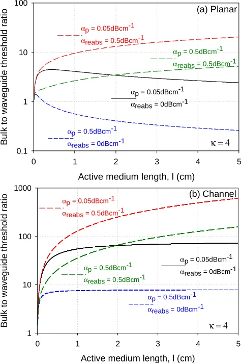
Plots of the bulk to waveguide threshold-power ratio as a
Fig. 2. Comparison between the laser threshold power for a bulk active medium with optimum focusing and the same media in a (a) planar and (b) channel waveguide configuration.
(b) Channel
Active medium length, l (cm)
0 1 2 3 4 5
B u lk t o w a v e g u id e t h re s h o ld r a ti o 1 10 100 1000
κ = 4
αp = 0.5dBcm-1
αreabs = 0dBcm-1
αp = 0.05dBcm-1
αreabs = 0dBcm-1
αp = 0.5dBcm-1 αreabs = 0.5dBcm-1
αp = 0.05dBcm-1
αreabs = 0.5dBcm-1
(a) Planar
Active medium length, l (cm)
0 1 2 3 4 5
B u lk t o w a v e g u id e t h re s h o ld r a ti o 0.1 1 10 100
αp = 0.05dBcm-1
αreabs = 0.5dBcm-1
αp = 0.5dBcm-1 αreabs = 0.5dBcm-1
αp = 0.05dBcm-1
αreabs = 0dBcm-1
αp = 0.5dBcm-1
[image:2.595.307.544.358.714.2]function of the active medium length, are shown in Fig. 2(a) and (b) for planar and channel waveguides respectively, assuming an output coupling four times the round trip losses i.e. κ = 4. Several assumptions have been made for this example, in addition to those detailed in references [13, 14]; firstly the common intrinsic cavity loss is set to Li = 0.01;
secondly, each waveguide was taken to have a full core width d = 7.5µm; and finally the vacuum pump wavelength was set to be 0.8µm with an active medium refractive index, np = 1.8.
In Fig. 2 we see that longer active media without re-absorption loss (αreabs = 0dBcm-1) show practically no
advantage if the propagation losses are high, especially for the planar guiding structures. In fact there is an optimum length (in the case of Fig.2(a) at <0.1cm for the higher loss example αp = 0.5dBcm-1 and ~0.5cm for the lower loss
example αp = 0.05dBcm-1) after which the contribution from
the propagation losses outweighs the benefits of optical confinement. However, for active materials with re-absorption loss there is a significant advantage to be gained by guiding the pump and laser radiation, especially for propagation losses comparable to or smaller than the re-absorption loss (αp < αreabs). A value of αreabs = 0.5dBcm-1 was selected for the
re-absorption loss as it is representative of efficient quasi-three-level materials, for example ~1at.% Ytterbium-doped YAG at room temperature.
Returning to the historical review, initial demonstrations of glass thin-film structures were only to show net gain [15, 16], with no report of laser action. Instead epitaxial growth of crystalline layers was rather more successful, with the first planar crystalline waveguide laser reported by Van der Ziel et al in 1972. The device was a Ho3+ doped Yttrium Aluminum Garnet (YAG) waveguide grown on a YAG substrate via liquid-phase-epitaxy (LPE) [17]. This favorable outcome was most likely due to the combination of lower propagation losses and the intrinsically higher gain of the activated crystalline material with respect to that of glass hosts. In the following years the same group reported improved results and also Nd3+ doped structures [18, 19], while in Germany at the Seimens Research Laboratories, the first hetro-epitaxial Nd:YAG films were grown on sapphire [20]. Like the earliest glass films these active guides were demonstrated to have net gain only. Grabmaier et al soon reported laser action from similar homo-epitaxial structures, to those reported in [18], but with propagation losses <0.5dBcm-1 [21]. These initial successes paved the way for the future development of solid-state dielectric planar waveguide lasers.
As an intriguing aside, it was again around the beginning of the 70’s that planar-waveguides found application with gaseous active media as well [22], where well-understood techniques such as electric or RF discharges could be used as an efficient excitation mechanism. Although based on hollow-waveguides and leaky modes as discussed by Degnan [23], optimization of the geometry led to reasonable propagation losses and ultimately efficient laser operation.
Continued growth of this research field during the following years, especially in the high-power arena, led to the first 1-kW class planar-waveguide CO2 laser demonstration two
decades later [24]. To date commercial CO2 lasers are the
market leaders for high-power lasers targeting materials processing applications [25], with manufacturers such as Trumpf Laser Division [26] offering systems with output powers up to 20kilowatts. This progression in the performance of the CO2 slab laser is representative of the
potential that the planar geometry has for solid dielectric active media, where uniform pumping and good thermal management are critical for high-power applications [27].
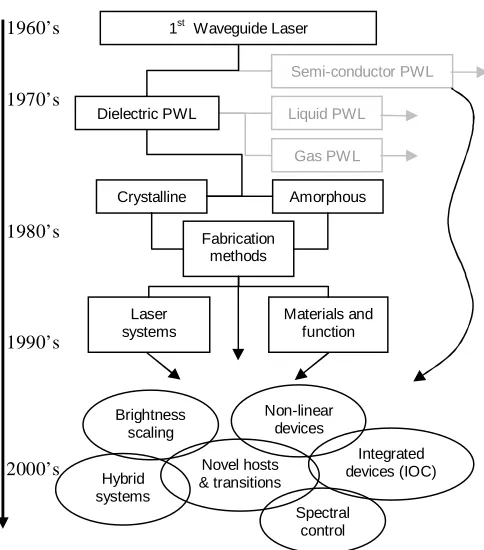
To attempt to follow a consistent thread amongst all of the divergent PWL technologies becomes unmanageable from the mid 90’s onwards. Instead, a few key results from some of the fields of research, indicated at the bottom of Fig. 3, will be highlighted, primarily those that exemplify the advantages of the planar waveguide laser.
B. Integrated Devices
Prior to the realization of the planar waveguide laser the concept of integrated optical circuits was already being defined [34]. The ability to control and manipulate light which is insensitive to the external environmental conditions, was considered highly attractive. Photonic circuits were envisaged with passive transmission lines that coupled functional devices including oscillators, modulators, and filters, all on the same chip. Such devices have since been realized [35-38] where telecommunication applications have been the primary motivation. A broad overview of this field can be found in Vol. 6, Issue 1 (2000) of this journal.
Research on active planar devices, for the most part, concentrated on compact amplifiers which looked to have the potential for compact multi-channel devices; however, there were also advocates for the PWL as the front end optical source in place of laser diodes. Their reasons included the unique properties of dielectric PWL’s, such as narrow linewidth, energy storage and therefore potentially high peak powers, and wavelength accessibility [39]. However, without the realization of practical devices to date, semiconductor PWL’s have proved themselves better equipped for the task.
To warrant the attention of real applications in the 1.55µm region, planar waveguide amplifiers and oscillators require high Erbium doping levels to provide sufficient gain with efficient pump absorption and short device lengths, unfortunately this leads to ion clustering and cooperative-upconversion processes that quench the 4I13/2 metastable
energy manifold thus reducing its lifetime [40]. Co-doping with Ytterbium was shown to facilitate shortening device lengths through exploiting its stronger absorption at around 0.97µm that could then efficiently transfer energy to the 4I11/2
manifold of Erbium. A fast relaxation to the 4I13/2 level [40]
provides the necessary inversion with a higher effective absorption cross section than single doping alone. However, cooperative upconversion processes were found to increase with co-doped hosts, once again limiting the Erbium concentration and possible overall system gain at 1.55µm. The demonstration of the Erbium doped fiber amplifier (EDFA), its longer lengths and low doping level, yet high potential gain, slowed interest in planar devices in spite of their applicability to IOC’s.
Recently another promising candidate, Er-doped silica containing nano-crystalline silicon (nc-Si) sensitizers, again with enhanced pump absorption for the Erbium ions has revived some interest in planar amplifiers once more [41, 42]. Strong broadband absorption in the visible spectrum by the nc-Si transfers to the narrow emission band of Erbium very efficiently, displaying orders of magnitude better effective absorption than traditional pumping of the Erbium 4f manifolds. This technology promises devices that can be face pumped with cheap LED sources and are compatible with silicon substrates.
Another host material extensively investigated for IOC applications is LiNbO3. Its ferroelectric properties allow
complex and fully integrated devices on the one substrate, enabling mode-locking [43], Q-switching [44], or even wavelength tuning [37] of monolithic PWL’s. Becker et al. make an excellent review of progress up until the late 90’s, made with Erbium-doped devices [45], with more recent devices reported by Sohler et al. [46]. Planar waveguide lasers based on this host have been demonstrated with various dopants (see Table 1), including monolithic lasers with intra-cavity quasi-phase-matched second-harmonic generation [47].
Ion exchange in glasses is another method for fabricating IOC devices which, while not having the high intrinsic gain of crystals or the ferroelectric properties of LiNbO3 does have
the benefit of simple waveguide fabrication with low-loss, either on active or passive substrates, or hybrid substrates that combine the two [48]. The resulting waveguides can be configured to have an excellent spatial mode overlap with standard optical fibers, and very low birefringence properties. Honkanen et al. [49] have very recently made a review on ion exchanged glass devices, in which they discuss new applications arising in biological sciences, and for sensors that utilize the waveguide evanescent field in a cladding
1st Waveguide Laser
Gas PWL Liquid PWL
Crystalline Amorphous
Fabrication methods
Laser systems
Integrated devices (IOC) Materials and
function Dielectric PWL
Semi-conductor PWL
Brightness scaling
Non-linear devices
Novel hosts & transitions Hybrid
systems
[image:4.595.48.290.85.360.2]Spectral control
Fig. 3. Development timeline for dielectric planar waveguide lasers, leading to a host of applications driven interdisciplinary research fields.
1970’s
1980’s
1990’s
medium to interact with the target components. For these devices it is preferable that there is a small index difference between the waveguide and media of interest, typically an aqueous solution or polymeric layer, so that the field can extend further into the cladding and thus increase the interaction volume. Therefore, these devices are ideally suited to glass rather than crystalline media. Integrated devices including multiple oscillators [38] and sensors are conceivable, where intra-cavity fields enhanced by the finesse of a laser resonator, may also improve the sensing efficiency.
C. Novel Hosts and Transitions
From the outset, planar waveguide lasers have provided a means to access laser transitions that can be difficult to realize in equivalent bulk configurations, e.g. Ho3+:YAG [17]. As discussed above, the impetus for research on compact planar amplifiers was the continual expansion of long-distance communications networks, where optical transitions within the optical-fiber transmission windows, around 1.3µm and 1.55µm, were of particular interest. Erbium is the rare earth ion of choice for the longer wavelength window, while Neodymium and Praseodymium are suitable for the lower window. Improvements in optical fiber properties and the advent of the EDFA meant that interest in planar structures for telecommunication applications waned. In its place,
attention returned to the advantages of the guiding geometry for oscillators, and the ability to fabricate planar structures with a variety of novel hosts and a range of active ions eventuating in an explosion of papers describing new PWL’s during the 90’s.
Table I is an incomplete list of reported laser action for several hosts doped with different active ions. The list includes many references that are noteworthy for their novelty, or offer significant performance improvements rather than being an exhaustive overview. As for bulk activated media, Neodymium is the most popular ion for demonstrating laser action in a new host media, Erbium follows with a reasonable second, although Ytterbium for which the waveguide geometry has particular advantage is likely to overtake in the near future.
Intrinsic to the PWL with relatively low-loss is low threshold power, even for active media with weak emission cross sections. This has enabled efficient PWL’s based on LiNbO3, fluoride crystals, and glass hosts, with references
listed in Table 1, in addition to stimulated emission from unusual transitions such as the 4F3/2→4I15/2 1.8µm line of
Neodymium [50], which is ~70 times weaker than the dominant 1.06µm transition in a YAG host.
TABLEI
ACTIVE WAVEGUIDE HOST MEDIA AND REPORTED LASER ACTION
Host media Nd3+ Er3+ Tm3+ Yb3+ Other
Oxides
YAG CW 0.94 [3, 50] CW 1.06 [28, 50-56] QS 1.06 [57] CW 1.3 [50, 58] CW 1.8 [50]
CW 1.55 [59] CW 2.7 [60]
CW 2.0 [61, 62] CW 1.03 [53, 57, 63-65] QS 1.03 [66]
QCW Ho3+ 2.1 [18]
GGG CW 0.94 [67, 68] CW 1.06 [67-72]
CW 1.03 [73]
Y2SiO5 CW 1.06 [74]
Al2O3 QCW Ti3+ 0.8 [75, 76]
GdVO4 CW 1.06 [77]
LiNbO3 CW 0.9 [78]
CW 1.08[79-81] QS 1.08 [82] ML 1.08 [35]
CW 1.55 [83, 84] QS 1.55 [44] T 1.55 [37] ML 1.55 [43]
CW 1.8 [85, 86] CW 1.06 [87, 88]
LiTaO3 CW 1.06 [89]
Fluorides
YLF CW 1.05 [90] LaF2 CW 1.06 [91]
CW 1.3 [92]
Tungstate
KYW CW 1.03 [93]
Glasses
Silicates CW 1.06 [94] CW 1.55 [95] Borosilicate CW 1.06 [10, 96-98] CW 1.55 [99] Phosphates QS 1.06 [100] CW 1.55 [101]
ML 1.55 [102]
Format: Mode of operation, wavelength in microns, reference.
D. Brightness Scaling
In this final part of our historical review, we note that the power levels of the previously discussed results were all relatively low. In fact breaking the 1Watt barrier by a solid-state dielectric PWL had to wait until approximately 10 years ago, when a diode-face-pumped 200µm thick multi-mode Nd:YAG/YAG composite planar waveguide, produced 9W average-power in quasi-continuous-wave (QCW) mode at Heriott Watt University [103]. Workers at Southampton University were soon to report multi-watt CW output powers from diode-end-pumping Nd:YAG PWL’s, the first consisting of a multi-mode (80µm) LPE grown core on a YAG substrate [104], and the second a slightly multi-mode (8µm) core clad with sapphire, fabricated using the direct-bonding technique [105]. Griebner et al. improved the PWL brightness by using extended cavities and various planar and channels structures again fabricated by the direct-bonding technique [65, 106].
Considering the increasing PWL’s power levels, it is worth highlighting the important diode-laser pump source parameters required by the guiding structure. As illustrated in Fig. 1. two generic pumping schemes can be adopted for exciting the active core of a planar waveguide. Face pumping offers a seemingly simple area-scalable pumping architecture, however, it is at the expense of engineering complexity, where an efficient reflective pump chamber is required that not only recycles the unabsorbed light back into the waveguide core, but also provides a robust low-stress method to cool the active medium. This technique provides a uniform pump distribution in the thick waveguide core, and using a low numerical aperture (NA) waveguide, reasonable overlap with the fundamental mode is achieved. On the other hand, edge pumping has a generic compatibility with high-power laser-diode arrays (bars), due to their good beam quality in the fast axis, which can be launched into the waveguide, while the slow axis beam can simply be conditioned to produce a uniform pumping distribution in the plane. Longitudinal-edge pumping can provide good efficiency, if configured to have a good mode-overlap between the doped area (or pump distribution) and signal fields, with respect to absorbed power but is only moderately power scalable. However, increasing diode-pump power typically belies degradation of its beam quality, through needing to stack bars in a vertical array; therefore, little can be gained for a near-single mode waveguide laser due to a decreasing launch-efficiency, unless a cladding-pumped structure is employed. In contrast edge-pumping in the transverse direction also offers a route to power-scaling, unfortunately however, at the expense of efficiency for near diffraction-limited outputs [51], due to the reduced mode-overlap between the distribution of the pump and signal fields. Finally, to achieve a good launch efficiency for the edge pumping schemes the pump beam quality, Mp2, should follow the relationship [105],
p
p NA D
M 2 < ⋅ λ , (2)
the aperture, D, can either be the core, d, or the outer cladding width of a double-clad structure.
In keeping with the concept of compact, robust and simple high-power sources, Bonner et al. reported the first monolithic double-clad planar waveguide lasers [53]. Multi-watt output powers were observed with Yb3+ and Nd3+ doped YAG cores, with diffraction-limited beam quality in the guided axis. These YAG/sapphire composite structures were pushed into the 10W regime with Nd3+, Yb3+ [57], and Tm3+ [62]. Although diffraction-limited in the guided axis, the beam quality in the unguided axis was quite poor. Beach et al. also describe their results of improved beam quality in the plane, obtained using a monolithic strip unstable resonator [57]. End-pumping these double-clad structures with high-brightness beam-shaped diodes was also shown to improve the beam quality and provide efficient operation [50].
Continued advancements with the face-pumped geometry at Heriott-Watt University, have shown output powers increased an order of magnitude further to 150W in multi-mode operation and >100W in a high-brightness configuration using an external negative-branch unstable resonator [54]. Similar thick-waveguide structures were used in self-imaging (Talbot imaging) configurations for lasers and amplifiers [107-109], while Sueda et al. [110] have demonstrated >250W with a diode-stack end-pumped few-hundred microns thick Yb:YAG core clad with sapphire, in what they termed a micro-thickness slab laser. As highlighted by Sueda et al. [110] the temperature gradient across the waveguide core can in fact be extremely low, despite these high powers.
To conclude this section it is worth reviewing why a low temperature gradient is important and how the planar waveguide provides additional benefit. The first relates to the maximum thermal load imposed by stress fracture in a uniformly heated slab, which Eggleston et al. [8] have discussed in detail, showing that it scales with the ratio of the larger surface area, A, to the thickness, t, that is the maximum thermal power is given by:
t A R
P s
therm slab 12
max_ = , (3)
where Rs is the thermal stress resistance and depends upon
the material properties of the host [8]. Taking the slab geometry to the extreme, one arrives at a waveguide structure and, introducing cladding layers such that the thermal load is confined to the core in the centre of the slab, we find that the stress-fracture thermal-power limit has the same proportionality, but reduced by a factor of 2/3 [111].
t A R
P s
therm wg 8
max_ = . (4)
Note however, this is actually a substantially higher thermal load density, Qmax, than the comparable slab, as heat
the minor temperature profile across the core, as long as the propagating mode is smaller than that of the thermal guide [109]. Following this reasoning, the benefit of a small waveguide core can be realized noting an inverse cubic dependence where the maximum thermal load for index guiding can be expressed by [111]:
(
)
32 2 _
max_ k A ndn dT d
P l
therm lens
wg ≈ λπ . (5)
New terms include the thermal conductivity of the material (assuming the same for core and cladding), k, and the change in refractive index as a function of the temperature, dn/dT. Taking the ratio of (5) and (4) we find that, for a typical YAG waveguide structure, core sizes below ~100µm are limited by stress fracture rather than thermal guiding. A similar structure of thickness t = 1mm can tolerate a thermal flux of up to ~640Wcm-2 according to (4) with Rs ~8Wcm-1 [8].
III. FABRICATION TECHNIQUES
Planar waveguide fabrication falls under two broad headings, modification of the refractive index of a bulk material, or layering or structuring materials with dissimilar refractive index. The first can be obtained through processes such as proton- or ion- exchange [4, 49, 112], ion-diffusion [113], ion-implantation [114], or optical writing methods [115-117]. Typically, these techniques, with exception of the last, form relatively thin waveguides with low numerical apertures and therefore are not compatible with highly divergent or multimode laser diode radiation for high-power applications. In contrast, the second fabrication methodology allows relatively thick guides of high index contrast and therefore high-NA waveguide structures. Techniques utilized to fabricate composite structures of dissimilar materials include; growth through epitaxial processes (Molecular Beam Epitaxy (MBE), LPE and PLD) [5-7], sputtering [118] or
deposition [119], material removal such as ion-beam milling [120] or etching [121], or simply adhesion [122, 123].
Active optical fibers can be made with extremely low propagation losses on the order of several dBkm-1 [33] therefore allowing long (>10m) fiber lengths with low active ion concentrations thus avoiding concentration quenching effects. The planar geometry is typically limited to lengths on the centimeter scale by fabrication and practical device size, which fortunately implies losses can be several orders of magnitude higher ≤0.1dBcm-1 without compromising laser performance in these shorter devices. As illustrated in the threshold comparison at the beginning of the section. Notwithstanding, propagation losses of this order can still be very challenging for many planar waveguide fabrication methods. Table II details several fabrication methods, indicating which host materials they are suited to, an order of magnitude indication of the index difference achieved, and typical reported propagation losses.
In light of Table II it is appreciated that there are several techniques from which to choose for making active planar waveguides. In fact, many more variations come under these listed headings. The host material that is applicable to an intended application will inevitably dictate the fabrication process; however, the key technologies are those that offer the lowest losses to the propagating modes. These include ion-exchange and optical writing for glass materials, while for crystals it is LPE, adhesion (direct bonding), with potential for ion-diffusion in some. Pulsed laser deposition (PLD) is also a technique that is showing promise with recent thick films of low loss (0.1dBcm-1) being reported [135].
Ion-exchange produce a graded refractive index change from the surface of the layer into the substrate, although the use of an annealing step with an applied electric field can bury the waveguide. This step is used to symmetrise the mode and decrease the propagation losses. Graded waveguides typically have quite wavelength dependent spatial modes, with higher order modes perpendicular to the plane extending well into the substrate due to the smaller index difference in that direction. Typically, this implies a poor spatial overlap with the signal fundamental mode and that of a less-than-diffraction-limited pump source. Consequently, these waveguide devices normally require high-brightness pump sources for efficient end-pumped laser operation. Adiabatic tapers have been demonstrated with good effect in transforming a single mode channel into a larger multimode channel [98, 101], which have the potential for single-emitter diode-pumping for compact 1W level devices. Moreover the additional functionality that can be integrated onto the planar substrate, as discussed above, offers these lasers sources a choice for their mode of operation with potential to meet many different requirements.
Epitaxial growth methods, such as LPE and PLD, require lattice matching between the various crystal layers to prevent dislocation defects in the film, which can ultimately lead to TABLEII
COMPARISON OF FABRICATION TECHNIQUES AND PROPAGATION LOSSES
Fabrication technique
Host
materials Index step
Typical propagation loss dBcm-1
Ref.
Ion-exchange Glass 10-3-10-2 0.1 [4, 49]
Proton-exchange LiNbO3,
LiTaO3
10-2 0.2 [89, 112,
124] Ion-diffusion LiNbO3
Sapphire 10-4
10-4
0.2 1
[125] [45, 126]
[127] Ion-implantation Crystal -3x10⁻² 1 [74, 114]
Optical Writing Glass 10-3-10-2 0.1-1 [117, 128]
LPE Crystal 10-3 0.1 [5, 93]
MBE Crystal 10-3 1 [91, 129]
Sputtering Amorph. 10-3-1 0.2 [130]
CVD Glass 10-2 0.01* [131]
FHD Glass 10-3 0.01*-0.8 [119, 132, 133]
PLD Crystal 0.1 1 [7]
Sol-gel Glass 0.14 1 [134]
Adhesion Crystal 10-4-0.2 0.1 [111]
cracks or be a source of scattering loss. Low-loss waveguiding layers are usually the result of careful optimization of the growth parameters and constituents that compensate for the different ionic radii and hence lattice deformation of the active ion substitute [5]. Therefore, as a powerful low-loss waveguide fabrication process, it is limited to hosts that have similar lattice parameters to the substrate, or which can be modified with additional substitutions without severely affecting the spectroscopy of the active ion. In some fortuitous situations different crystals such as Nd:GGG and YAG have such a correspondence, as demonstrated by May-Smith et al. [135], enabling a high index contrast and high numerical aperture waveguide structures with the potential for multi-layered structures and high-power diode pumping [72].
The final waveguide fabrication technique discussed here is that of direct bonding. Not a growth technique, it uses prefabricated high-quality optical materials that are precision-polished flat, chemically treated to provide a clean hydrophilic surface, then brought together with a second similarly prepared surface. Van der Waal’s bonding initiates when the surfaces are in close proximity, commonly known as contact bonding, however, a further thermal annealing step allows stronger covalent bonds to form and the composite is no longer susceptible to delamination through shock. Limited eventually to materials with similar thermal expansion coefficients there is still reasonable flexibility in material choice by not having to lattice match layer and substrate.
The last two fabrication techniques can be used to make double-clad waveguide structures, illustrated in Fig 4, where a near single-mode active core is encapsulated by a larger highly multimode waveguide, similar to double-clad optical fibers. These structures enable high-power diode pumping as discussed in Section IID, and also force single-mode operation in the guided plane despite the highly multi-mode nature of the complete structure [136]. The drawback of the double-clad waveguide is the increase in the absorption length, scaling approximately with the ratio of the core thickness, d, to that of the overall waveguide aperture, D [137]. Therefore, for reasonable device lengths it is important to maintain this ratio close one, or use active materials with
large absorption cross section.
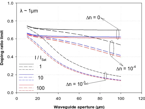
Bhutta et al. [136] demonstrated that for d/D<0.6, gain saturation across the active core by the fundamental mode prevents higher order modes from reaching threshold. Accounting for an increase in the core refractive index with respect to the inner cladding, typically associated with the introduction of a rare earth ion, and the subsequent reduction in mode size due to the stronger confinement, we see that this optimum ratio is decreased [60], Fig 5. Although this plot is for 1-micron radiation and a core refractive index ncore~1.8,
the optimum ratio for other wavelengths, for the same core index, is found by scaling the bottom axis by 1/λother (with λother in microns). For other values of core refractive index, a
further scaling factor is required, that is NAother/NAcore, where
NAcore = 0.019 and 0.06 for ∆n=10-4 and 10-3 respectively.
From Fig. 5 it is noted that scaling to larger waveguide dimensions to facilitate high-power diode pumping requires extreme control of the index contrast between the core and inner cladding layers. Large-mode-area fiber is the analogue technology where the core refractive-index-profile is designed to increase the size of the fundamental mode [138]. Recently there have been new proposed techniques for fundamental-mode selection from highly multi-fundamental-mode planar waveguides [139, 140], however, this problem is not yet fully resolved and leads us into the following section.
IV. CHALLENGES AHEAD
There have been many advantages of the planar waveguide laser highlighted above, however, for these laser devices to achieve their full potential there are a few disadvantages that still need to be addressed. Influence on the current state-of-the-art high-power application for the PWL comes from two sides, one trying to reduce the overall structure size thus optimizing the output within the limits imposed by stress-fracture and thermal lensing, while the other is trying to increase the waveguide dimension to enable pumping with higher powers. In addition, scaling the output powers further,
Waveguide aperture (µµµµm)
0 20 40 60 80 100 120
D
o
p
in
g
r
a
ti
o
l
im
it
0.0 0.2 0.4 0.6 0.8 1.0
I / ISat
1
10
100 ∆n = 10 -3
∆n = 10-4
∆n = 0
[image:8.595.47.287.83.238.2]λ ~ 1µm
Fig. 5. Doping ratio limit as function of waveguide aperture.
n
y
nInner cladding
nActive core Re:YAG
YA Sapphire
y
nOuter cladding
Active core
Inner cladding
d
D
[image:8.595.307.544.272.451.2]Outer cladding
efficiently, requires consideration of the restrictions imposed by pump launch efficiency, the thermal load and ability to remove all the localized waste heat, and the overall losses introduced with guided propagation. While spatial mode control in the guided direction has been successfully demonstrated in monolithic cavities using double-clad structures, going to large waveguide dimensions will require additional methods to ensure diffraction-limited operation, such as self-imaging techniques, and extended cavity configurations. All the while the beam quality in the unguided dimension also remains a topic for discussion, unstable resonators have so far been the only successful method found for making near diffraction-limited output in this plane. Moreover, to take full advantage of the immunity to the local environment requires the resonator be monolithic with the waveguide.
Further reduction in the propagation losses and hence total cavity losses for PWL’s is essential for efficient operation of devices greater than a few centimeters. For example to get a slope efficiency of 95% of the maximum possible, i.e. the Stokes efficiency for lasers without quantum yield enhancement through excited-state energy transfer processes, requires κ = 19, that is the optimum output coupling needs to be this many times larger than the cavity losses. Again, planar waveguide lasers find themselves in the middle ground, with respect to an unguided configuration optical confinement in one plane provides linear enhancement of the small signal gain whereas two degrees of confinement gives quadratic improvement. There is still strong potential for active planar waveguides however, particularly for high average-power devices, where the optimum output coupling can be quite high. This is the reason that CW fiber-lasers can be extremely efficient, as a ~4% output coupling leads to κ ≈ 30 for cavity losses of 10%. Notwithstanding, PWL’s can have equivalent CW performance if there is an order of magnitude improvement on the typical propagation losses to ~0.01dBcm-1. At present, the best LPE losses are around 0.04dBcm-1.
Although not discussed above, amplified spontaneous emission can be problematic for guided-wave lasers. Due to the combination of high gain and the waveguide NA that captures a portion of the omni-directional spontaneous emission. Essentially increasing the path length over which the fluorescence overlaps the excitation volume. Although typically not a problem for low threshold CW lasers, it can sometimes lead to spurious parasitic lasing paths that extract some of the available inversion. In the worst case, this can prevent the laser reaching threshold. Circumventing ASE losses is even more difficult in Q-switched lasers with large inversion densities. There have been various techniques demonstrated for minimizing the ASE content [57, 110], however, it is can still be challenging for the PWL designer.
Finally for IOC type devices, there are several challenges ahead revolving around integrating various active and passive
devices onto the one substrate that supports their function and has a low loss-penalty. Furthermore, to have a compact chip containing many devices will require waveguide structures that can support small bend radii in the plane; this requires high index-contrast guides. To date the photonic analogue to silicon is still to be identified, although there are many candidates currently being investigated.
V. CONCLUSION
In this paper we have seen the enormous variety of planar waveguide laser systems that have now been now realized. From the very early days following the inception of the laser, active guided structures found a role in many of the major developments leading to novel coherent optical sources. Valuable for their potentially low thresholds and suitability for quasi-three-level transitions, the active planar waveguide lays on the middle ground between its bulk and fiber analogues. Allowing it to exploit the attributes for which these other gain media excel, such as energy storage in a bulk active medium or the high gain and efficient CW performance of fiber lasers. Additional benefits derived from its planar geometry include, the natural compatibility with high-power diode-lasers and, excellent thermal management qualities, particularly for thin waveguide structures.
The extensive range of fabrication techniques available for thin active films has enabled the PWL to function in many different modes of operation, in both the temporal and spectral regimes, while even being in the race for high average-powers. Moreover, these lasers are well on their way to integration on single substrates with other functional devices that provide the abovementioned qualities from efficient, compact, and robust packages.
ACKNOWLEDGMENT
The author wishes to express his gratitude to Professors D.P. Shepherd and W.A. Clarkson, their input, guidance, and influence have been invaluable.
REFERENCES
[1] E. Snitzer, Physics Review Letters, vol. 7, pp. 175 -177, 1961.
[2] M. J. F. Digonnet and C. J. Gaeta, "Theoretical-Analysis of Optical Fiber Laser-Amplifiers and Oscillators," Applied Optics, vol. 24, pp. 333-342, 1985.
[3] D. C. Hanna, A. C. Large, D. P. Shepherd, A. C. Tropper, I. Chartier, B. Ferrand, and D. Pelenc, "Low-Threshold Quasi-3-Level 946nm Laser Operation of an Epitaxially Grown Nd:Y3Al5O12 Wave-Guide," Applied Physics Letters, vol. 63, pp. 7-9, 1993.
[4] R. V. Ramaswamy and R. Srivastava, "Ion-Exchanged Glass Wave-Guides - a Review," Journal of Lightwave Technology, vol. 6, pp. 984-1002, 1988.
[5] B. Ferrand, B. Chambaz, and M. Couchaud, "Liquid phase epitaxy: A versatile technique for the development of miniature optical components in single crystal dielectric media," Optical Materials, vol. 11, pp. 101-114, 1999.
[6] R. Burkhalter, I. Dohnke, and J. Hulliger, "Growing of bulk crystals and structuring waveguides of fluoride materials for laser applications,"
Progress in Crystal Growth and Characterization of Materials, vol. 42,
[7] M. Jelinek, "Progress in optical waveguiding thin films," Czechoslovak
Journal Of Physics, vol. 53, pp. 365-377, 2003.
[8] J. M. Eggleston, T. J. Kane, K. Kuhn, J. Unternahrer, and R. L. Byer, "The Slab Geometry Laser .1. Theory," IEEE Journal of Quantum
Electronics, vol. 20, pp. 289-301, 1984.
[9] H. Kogelnik and C. V. Shank, "Stimulated Emission in a Periodic Structure," Applied Physics Letters, vol. 18, pp. 152-&, 1971.
[10] J. E. Roman and K. A. Winick, "Neodymium-Doped Glass Channel Wave-Guide Laser Containing An Integrated Distributed Bragg Reflector," Applied Physics Letters, vol. 61, pp. 2744-2746, 1992. [11] G. Zeidler, "Optical waveguide technique with organic dye lasers,"
Journal of Applied Physics, vol. 42, pp. 884-5, 1971.
[12] J. P. Wittke, "Thin-film lasers," RCA Review, vol. 33, pp. 674-94, 1972. [13] K. Kubodera and K. Otsuka, "Single-transverse-mode LiNdP4O12 slab
waveguide laser," Journal of Applied Physics, vol. 50, pp. 653-659, 1979. [14] T. Taira, W. M. Tulloch, and R. L. Byer, "Modeling of quasi-three-level lasers and operation of CW Yb:YAG lasers," Applied Optics, vol. 36, pp. 1867-1874, 1997.
[15] H. Yajima, Y. Sekimoto, and S. Kawase, "Amplification at 1.06µm Using a Nd - Glass Thin-Film Waveguide," Applied Physics Letters, vol. 21, pp. 407-&, 1972.
[16] B. U. Chen and C. L. Tang, "Nd-Glass Thin-Film Waveguide - Active Medium for Nd Thin-Film Laser," Applied Physics Letters, vol. 28, pp. 435-437, 1976.
[17] J. P. van der Ziel, L. G. Vanuiter, W. A. Bonner, and L. Kopf, "Coherent Emission from Ho3+ Ions in Epitaxially Grown Thin Aluminum Garnet Films," Physics Letters A, vol. A 42, pg. 105, 1972.
[18] J. P. van der Ziel, W. A. Bonner, L. Kopf, S. Singh, and Vanuiter.Lg, "Laser Oscillation from Ho3+ and Nd3+ Ions in Epitaxially Grown Thin
Aluminum Garnet Films," Applied Physics Letters, vol. 22, pp. 656-657, 1973.
[19] W. A. Bonner, "Epitaxial-Growth of Garnets for Thin-Film Lasers,"
Journal of Electronic Materials, vol. 3, pp. 193-208, 1974.
[20] J. G. Grabmaier, B. C. Grabmaier, R. T. Kersten, R. D. Plattner, and G. J. Zeidler, "Epitaxially Grown Nd Laser-Films," Physics Letters A, vol. A 43, pp. 219-220, 1973.
[21] J. G. Grabmaier, R. D. Plattner, P. Mockel, and W. W. Kruhler, "Liquid-Phase Epitaxy of Nd3+-doped YAG Layers by Dipping Technique," Journal of Crystal Growth, vol. 34, pp. 280-284, 1976.
[22] P. W. Smith, "A waveguide gas laser," Applied Physics Letters, vol. 18, pp. 152-154, 1971.
[23] J. J. Degnan, "Waveguide Laser - Review," Applied Physics, vol. 11, pp. 1-33, 1976.
[24] A. D. Colley, H. J. Baker, and D. R. Hall, "Planar Wave-Guide, 1kW CW, Carbon-Dioxide Laser-Excited by a Single Transverse RF Discharge," Applied Physics Letters, vol. 61, pp. 136-138, 1992. [25] K. Kincade and S. G. Anderson, "Market's messages are mixed. Low
growth overall in 2005 masks some strong performers." in Laser Focus
World, vol. 42, 2006, pp. 78-93.
[26] Trumpf, http://www.trumpf-laser.com, 2006.
[27] T. S. Rutherford, W. M. Tulloch, E. K. Gustafson, and R. L. Byer, "Edge-pumped quasi-three-level slab lasers: Design and power scaling," IEEE
Journal Of Quantum Electronics, vol. 36, pp. 205-219, 2000.
[28] P. J. Chandler, S. J. Field, D. Hanna, S. D.P., P. D. Townsend, A. C. Tropper, and L. Zhang, "Ion-Implanted Nd:YAG Planar Waveguide Laser," Electronics Letters, vol. 25, pp. 985-986, 1989.
[29] E. Lallier, J. P. Pocholle, M. Papuchon, C. Grezesbesset, E. Pelletier, M. Demicheli, M. J. Li, Q. He, and D. B. Ostrowsky, "Laser Oscillation of Single-Mode Channel Wave-Guide in Nd:MgO:LiNbO3," Electronics Letters, vol. 25, pp. 1491-1492, 1989.
[30] Y. Hibino, T. Kitagawa, M. Shimizu, F. Hanawa, and A. Sugita, "Neodymium-Doped Silica Optical Wave-Guide Laser on Silicon Substrate," IEEE Photonics Technology Letters, vol. 1, pp. 349-350, 1989.
[31] P. Mazzinghi, P. Burlamacchi, M. Matera, H. F. Raneasandoval, R. Salimbeni, and U. Vanni, "A 200-W Average Power, Narrow Bandwidth, Tunable Waveguide Dye-Laser," IEEE Journal of Quantum Electronics, vol. 17, pp. 2245-2249, 1981.
[32] S. B. Poole, D. N. Payne, and M. E. Fermann, "Fabrication of Low-Loss Optical Fibers Containing Rare-Earth Ions," Electronics Letters, vol. 21, pp. 737-738, 1985.
[33] R. J. Mears, L. Reekie, S. B. Poole, and D. N. Payne, "Neodymium-Doped Silica Single-Mode Fiber Lasers," Electronics Letters, vol. 21, pp. 738-740, 1985.
[34] S. E. Miller, "INTEGRATED OPTICS - AN INTRODUCTION," Bell
System Technical Journal, vol. 48, pp. 2059, 1969.
[35] E. Lallier, J. P. Pocholle, M. Papuchon, Q. He, M. Demicheli, D. B. Ostrowsky, C. Grezesbesset, and E. Pelletier, "Integrated Nd:MgO:LiNbO3 FM Mode-Locked Wave-Guide Laser," Electronics
Letters, vol. 27, pp. 936-937, 1991.
[36] J. Sochtig, H. Schutz, R. Widmer, R. Corsini, D. Hiller, C. Carmannini, G. Consonni, S. Bosso, and L. Gobbi, "Monolithically integrated DBR waveguide laser and intensity modulator in erbium doped LiNbO3,"
Electronics Letters, vol. 32, pp. 899-900, 1996.
[37] K. Schafer, I. Baumann, W. Sohler, H. Suche, and S. Westenhofer, "Diode-pumped and packaged acoustooptically tunable Ti:Er:LiNbO3 waveguide laser of wide tuning range," IEEE Journal of Quantum
Electronics, vol. 33, pp. 1636-1641, 1997.
[38] D. L. Veasey, D. S. Funk, N. A. Sanford, and J. S. Hayden, "Arrays of distributed-Bragg-reflector waveguide lasers at 1536 nm in Yb/Er codoped phosphate glass," Applied Physics Letters, vol. 74, pp. 789-791, 1999.
[39] E. Lallier, "Rare-Earth-Doped Glass and LiNbO3 Wave-Guide Lasers and
Optical Amplifiers," Applied Optics, vol. 31, pp. 5276-5282, 1992. [40] B. C. Hwang, S. B. Jiang, T. Luo, J. Watson, G. Sorbello, and N.
Peyghambarian, "Cooperative upconversion and energy transfer of new high Er3+- and Yb3+-Er3+-doped phosphate glasses," Journal of the Optical Society of America B-Optical Physics, vol. 17, pp. 833-839, 2000.
[41] M. Fujii, M. Yoshida, S. Hayashi, and K. Yamamoto, "Photoluminescence from SiO2 films containing Si nanocrystals and Er:
Effects of nanocrystalline size on the photoluminescence efficiency of Er3+," Journal of Applied Physics, vol. 84, pp. 4525-4531, 1998. [42] V. Y. Timoshenko, D. M. Zhigunov, P. K. Kashkarov, O. A. Shalygina,
S. A. Teterukov, R. J. Zhang, M. Zacharias, M. Fujii, and S. Hayashi, "Photoluminescence properties of erbium-doped structures of silicon nanocrystals in silicon dioxide matrix," Journal of Non-Crystalline Solids, vol. 352, pp. 1192-1195, 2006.
[43] R. Wessel, R. Ricken, K. Rochhausen, H. Suche, and W. Sohler, "Supermode stabilized coupled-cavity 5-and 10-GHz mode-locked Ti : Er:LiNbO3 waveguide lasers," IEEE Journal of Quantum Electronics, vol. 36, pp. 394-399, 2000.
[44] H. Suche, T. Oesselke, J. Pandavenes, R. Ricken, K. Rochhausen, W. Sohler, S. Balsamo, I. Montrosset, and K. K. Wong, "Efficient Q-switched Ti:Er:LiNbO3 waveguide laser," Electronics Letters, vol. 34, pp.
1228-1230, 1998.
[45] C. Becker, T. Oesselke, J. Pandavenes, R. Ricken, K. Rochhausen, G. Schreiber, W. Sohler, H. Suche, R. Wessel, S. Balsamo, I. Montrosset, and D. Sciancalepore, "Advanced Ti:Er:LiNbO3 waveguide lasers," IEEE Journal of Selected Topics in Quantum Electronics, vol. 6, pp. 101-113,
2000.
[46] W. Sohler, B. K. Das, D. Dey, S. Reza, H. Suche, and R. Ricken, "Erbium-doped lithium niobate waveguide lasers," IEICE Transactions
On Electronics, vol. E88C, pp. 990-997, 2005.
[47] M. Fujimura, T. Kodama, T. Suhara, and H. Nishihara, "Quasi-phase-matched self-frequency-doubling waveguide laser in Nd:LiNbO3," IEEE Photonics Technology Letters, vol. 12, pp. 1513-1515, 2000.
[48] S. D. Conzone, J. S. Hayden, D. S. Funk, A. Roshko, and D. L. Veasey, "Hybrid glass substrates for waveguide device manufacture," Optics
Letters, vol. 26, pp. 509-511, 2001.
[49] S. Honkanen, B. R. West, S. Yliniemi, P. Madasamy, M. Morrell, J. Auxier, A. Schulzgen, N. Peyghambarian, J. Carriere, J. Frantz, R. Kostuk, J. Castro, and D. Geraghty, "Recent advances in ion exchanged glass waveguides and devices," Physics And Chemistry Of
Glasses-European Journal Of Glass Science And Technology Part B, vol. 47, pp.
110-120, 2006.
[50] J. I. Mackenzie, C. Li, and D. P. Shepherd, "Multi-watt, high efficiency, diffraction-limited Nd:YAG planar waveguide laser," IEEE Journal of
Quantum Electronics, vol. 39, pp. 493-500, 2003.
[51] D. C. Hanna, A. C. Large, D. P. Shepherd, A. C. Tropper, I. Chartier, B. Ferrand, and D. Pelenc, "A Side-Pumped Nd:YAG Epitaxial Wave-Guide Laser," Optics Communications, vol. 91, pp. 229-235, 1992.
[52] I. Chartier, B. Ferrand, D. Pelenc, S. J. Field, D. C. Hanna, A. C. Large, D. P. Shepherd, and A. C. Tropper, "Growth and Low-Threshold Laser Oscillation of an Epitaxially Grown Nd:YAG Wave-Guide," Optics
Letters, vol. 17, pp. 810-812, 1992.
waveguide lasers," IEEE Journal Of Quantum Electronics, vol. 36, pp. 236-242, 2000.
[54] J. R. Lee, H. J. Baker, G. J. Friel, G. J. Hilton, and D. R. Hall, "High-average-power Nd:YAG planar waveguide laser that is face pumped by 10 laser diode bars," Optics Letters, vol. 27, pp. 524-526, 2002. [55] E. Flores-Romero, G. V. Vazquez, H. Marquez, R. Rangel-Rojo, J.
Rickards, and R. Trejo-Luna, "Planar waveguide lasers by proton implantation in Nd:YAG crystals," Optics Express, vol. 12, pp. 2264-2269, 2004.
[56] A. G. Okhrimchuk, A. V. Shestakov, I. Khrushchev, and J. Mitchell, "Depressed cladding, buried waveguide laser formed in a YAG:Nd3+
crystal by femtosecond laser writing," Optics Letters, vol. 30, pp. 2248-2250, 2005.
[57] R. J. Beach, S. C. Mitchell, H. E. Meissner, O. R. Meissner, W. F. Krupke, J. M. McMahan, W. J. Bennett, and D. P. Shepherd, "Continuous-wave and passively Q-switched cladding-pumped planar waveguide lasers," Optics Letters, vol. 26, pp. 881-883, 2001.
[58] M. Domenech, G. V. Vazquez, E. Flores-Romero, E. Cantelar, and G. Lifante, "Continuous-wave laser oscillation at 1.3µm in Nd:YAG proton-implanted planar waveguides," Applied Physics Letters, vol. 86, 2005. [59] D. P. Shepherd, D. Hanna, A. C. Large, A. C. Tropper, T. J. Warburton,
C. Borel, B. Ferrand, D. Pelnec, A. Rameix, P. Thony, F. Auzel, and D. Meichenin, "A low threshold, room temperature 1.64µm Yb:Er:Y3Al5O12
waveguide laser," Journal of Applied Physics, vol. 76, pp. 7651-7653 1994.
[60] J. I. Mackenzie, "High-Brightness Diode-Pumped Waveguide Lasers," in
Faculty of Engineering and Applied Science. Southampton: University of
Southampton, 2003, pp. 154.
[61] A. Rameix, C. Borel, B. Chambaz, B. Ferrand, D. P. Shepherd, T. J. Warburton, D. C. Hanna, and A. C. Tropper, "An efficient, diode-pumped, 2µm Tm:YAG waveguide laser," Optics Communications, vol. 142, pp. 239-243, 1997.
[62] J. I. Mackenzie, S. C. Mitchell, R. J. Beach, H. E. Meissner, and D. P. Shepherd, "15W diode-side-pumped Tm:YAG waveguide laser at 2µm,"
Electronics Letters, vol. 37, pp. 898-899, 2001.
[63] D. C. Hanna, J. K. Jones, A. C. Large, D. P. Shepherd, A. C. Tropper, P. J. Chandler, M. J. Rodman, P. D. Townsend, and L. Zhang, "Quasi-3 Level 1.03 µm Laser Operation of a Planar Ion-Implanted Yb:YAG Wave-Guide," Optics Communications, vol. 99, pp. 211-215, 1993. [64] D. Pelenc, B. Chambaz, I. Chartier, B. Ferrand, C. Wyon, D. P. Shepherd,
D. C. Hanna, A. C. Large, and A. C. Tropper, "High Slope Efficiency and Low-Threshold in a Diode-Pumped Epitaxially Grown Yb:YAG Wave-Guide Laser," Optics Communications, vol. 115, pp. 491-497, 1995. [65] U. Griebner and H. Schonnagel, "Laser operation with nearly
diffraction-limited output from a Yb:YAG multimode channel waveguide," Optics
Letters, vol. 24, pp. 750-752, 1999.
[66] J. I. Mackenzie and D. P. Shepherd, "End-pumped, passively Q-switched Yb:YAG double-clad waveguide laser," Optics Letters, vol. 27, pp. 2161-2163, 2002.
[67] C. L. Bonner, A. A. Anderson, R. W. Eason, D. P. Shepherd, D. S. Gill, C. Grivas, and N. Vainos, "Performance of a low-loss pulsed-laser deposited Nd:Gd3Ga5O12 waveguide laser at 1.06 and 0.94µm," Optics Letters, vol. 22, pp. 988-990, 1997.
[68] N. A. Vainos, C. Grivas, C. Fotakis, R. W. Eason, A. A. Anderson, D. S. Gill, D. P. Shepherd, M. Jelinek, J. Lancok, and J. Sonsky, "Planar laser waveguides of Ti:sapphire, Nd:GGG and Nd:YAG grown by pulsed laser deposition," Applied Surface Science, vol. 129, pp. 514-519, 1998. [69] S. J. Field, D. C. Hanna, A. C. Large, D. P. Shepherd, A. C. Tropper, P. J.
Chandler, P. D. Townsend, and L. Zhang, "An Efficient, Diode-Pumped, Ion-Implanted Nd:GGG Planar Wave-Guide Laser," Optics Communications, vol. 86, pp. 161-166, 1991.
[70] D. S. Gill, A. A. Anderson, R. W. Eason, T. J. Warburton, and D. P. Shepherd, "Laser operation of an Nd:Gd3Ga5O12 thin-film optical
waveguide fabricated by pulsed laser deposition," Applied Physics Letters, vol. 69, pp. 10-12, 1996.
[71] R. Gerhardt, J. Kleine-Borger, L. Beilschmidt, M. Frommeyer, H. Dotsch, and B. Gather, "Efficient channel-waveguide laser in Nd:GGG at 1.062µm wavelength," Applied Physics Letters, vol. 75, pp. 1210-1212, 1999.
[72] C. Grivas, T. C. May-Smith, D. P. Shepherd, and R. W. Eason, "Laser operation of a low loss (0.1 dB/cm) Nd:Gd3Ga5O12 thick (40µm) planar
waveguide grown by pulsed laser deposition," Optics Communications, vol. 229, pp. 355-361, 2004.
[73] M. Shimokozono, N. Sugimoto, A. Tate, Y. Katoh, M. Tanno, S. Fukuda, and T. Ryuoh, "Room-temperature operation of an Yb-doped Gd3Ga5O12
buried channel waveguide laser at 1.025µm wavelength," Applied Physics
Letters, vol. 68, pp. 2177-2179, 1996.
[74] J. H. Sharp, M. J. Rodman, P. J. Chandler, and P. D. Townsend, "Planar Optical Wave-Guides in Nd-Doped Yttrium Oxy-Orthosilicate," Applied
Physics Letters, vol. 64, pp. 2637-2639, 1994.
[75] A. A. Anderson, R. W. Eason, L. M. B. Hickey, M. Jelinek, C. Grivas, D. S. Gill, and N. A. Vainos, "Ti:sapphire planar waveguide laser grown by pulsed laser deposition," Optics Letters, vol. 22, pp. 1556-1558, 1997. [76] C. Grivas, D. P. Shepherd, T. C. May-Smith, R. W. Eason, and M.
Pollnau, "Single-transverse-mode Ti:sapphire rib waveguide laser,"
Optics Express, vol. 13, pp. 210-215, 2005.
[77] M. Imaki, S. Yamamoto, K. Seki, T. Yanagisawa, and Y. Hirano, "Diode proximity-coupled Nd:GdVO4 planar waveguide laser " in Conference on Lasers and Electro-Optics. Long Beach Convention Center: Optical
Society of America, 2006.
[78] C. T. A. Brown, J. Amin, D. P. Shepherd, A. C. Tropper, M. Hempstead, and J. M. Almeida, "900nm Nd:Ti:LiNbO3 waveguide laser," Optics Letters, vol. 22, pp. 1778-1780, 1997.
[79] E. Lallier, J. P. Pocholle, M. Papuchon, M. P. Demicheli, M. J. Li, Q. He, D. B. Ostrowsky, C. Grezesbesset, and E. Pelletier, "Nd:Mgo:LiNbO3
Channel Wave-Guide Laser Devices," IEEE Journal of Quantum
Electronics, vol. 27, pp. 618-625, 1991.
[80] S. J. Field, D. C. Hanna, D. P. Shepherd, A. C. Tropper, P. J. Chandler, P. D. Townsend, and L. Zhang, "Ion-Implanted Nd:MgO:LiNbO3 Planar
Wave-Guide Laser," Optics Letters, vol. 16, pp. 481-483, 1991. [81] M. Hempstead, J. S. Wilkinson, and L. Reekie, "Wave-Guide Lasers
Operating at 1084nm in Neodymium-Diffused Lithium-Niobate," IEEE
Photonics Technology Letters, vol. 4, pp. 852-855, 1992.
[82] E. Lallier, D. Papillon, J. P. Pocholle, M. Papuchon, M. Demicheli, and D. B. Ostrowksy, "Short-Pulse, High-Power Q-Switched Nd:MgO:LiNbO3 Wave-Guide Laser," Electronics Letters, vol. 29, pp.
175-176, 1993.
[83] P. Becker, R. Brinkmann, M. Dinand, W. Sohler, and H. Suche, "Er-Diffused Ti:LiNbO3 Wave-Guide Laser of 1563 and 1576nm Emission
Wavelengths," Applied Physics Letters, vol. 61, pp. 1257-1259, 1992. [84] J. Amin, J. A. Aust, and N. A. Sanford, "Z-propagating waveguide lasers
in rare-earth-doped Ti:LiNbO3," Applied Physics Letters, vol. 69, pp.
3785-3787, 1996.
[85] J. P. de Sandro, J. K. Jones, S. D.P., M. Hempstead, J. Wang, and A. C. Tropper, "Non-Photorefractive CW Tm-Indiffused Ti:LiNbO3 Waveguide
Laser Operating at Room Temperature," IEEE Photonics Technology
Letters, vol. 8, pp. 209-211, 1996.
[86] E. Cantelar, J. A. Sanz-Garcia, G. Lifante, and F. Cusso, "Single polarized Tm3+ laser in Zn-diffused LiNbO3 channel waveguides," Applied Physics Letters, vol. 86, 2005.
[87] J. K. Jones, J. P. Desandro, M. Hempstead, D. P. Shepherd, A. C. Large, A. C. Tropper, and J. S. Wilkinson, "Channel Wave-Guide Laser at 1µm in Yb-Indiffused LiNbO3," Optics Letters, vol. 20, pp. 1477-1479, 1995.
[88] M. Fujimura, H. Tsuchimoto, and T. Suhara, "Yb-diffused LiNbO3
annealed/proton exchanged waveguide lasers," IEEE Photonics
Technology Letters, vol. 17, pp. 130-132, 2005.
[89] S. Nouh, P. Baldi, K. Elhadi, M. Demicheli, G. Monnom, D. B. Ostrowsky, E. Lallier, and M. Papuchon, "Fabrication Parameter Optimization of a Low-Threshold High-Efficiency Proton-Exchanged Wave-Guide Laser in Nd-LiTaO3," Optics Letters, vol. 20, pp.
1468-1470, 1995.
[90] P. Rogin and J. Hulliger, "Epitaxial Nd:YLF linear waveguide laser,"
Optics Letters, vol. 22, pp. 1701-1703, 1997.
[91] E. Daran, D. P. Shepherd, T. Bhutta, and C. Serrano, "Laser operation of Nd:LaF3 thin film grown by molecular beam epitaxy," Electronics Letters,
vol. 35, pp. 398-400, 1999.
[92] X. Zhang, F. Lahoz, C. Serrano, G. Lacoste, and E. Daran, "1.3µm emission of Nd:LaF3 thin films grown by molecular beam epitaxy," IEEE Journal of Quantum Electronics, vol. 36, pp. 243-247, 2000.
[93] Y. E. Romanyuk, C. N. Borca, M. Pollnau, S. Rivier, V. Petrov, and U. Griebner, "Yb-doped KY(WO4)2 planar waveguide laser," Optics Letters,
vol. 31, pp. 53-55, 2006.
[94] A. K. Mairaj, X. Feng, D. P. Shepherd, and D. W. Hewak, "Channel waveguide lasers in a lead silicate glass fashioned using the extrusion technique," Applied Physics Letters, vol. 85, pp. 2727-2729, 2004. [95] P. M. Peters, D. S. Funk, A. P. Peskin, D. L. Veasey, N. A. Sanford, S. N.