Rochester Institute of Technology
RIT Scholar Works
Theses Thesis/Dissertation Collections
2010
Design and analysis of an FPGA-based,
multi-processor HW-SW system for SCC applications
Andrew Fitzgerald
Follow this and additional works at:http://scholarworks.rit.edu/theses
This Thesis is brought to you for free and open access by the Thesis/Dissertation Collections at RIT Scholar Works. It has been accepted for inclusion
in Theses by an authorized administrator of RIT Scholar Works. For more information, please [email protected].
Recommended Citation
Design and Analysis of an FPGA-based, Multi-processor
HW-SW System for SCC Applications
by
Andrew F. Fitzgerald
A Thesis Submitted in Partial Fulfillment of the Requirements for the Degree of Master of Science in Computer Engineering
Supervised by Dr. Marcin Łukowiak
Department of Computer Engineering Kate Gleason College of Engineering
Rochester Institute of Technology Rochester, New York
November 2010
Approved By:
Dr. Marcin Łukowiak
Assistant Professor, RIT Department of Computer Engineering Primary Adviser
Dr. Michael Kurdziel
Senior Engineering Manager, Harris Corporation Committee Member
Dr. Pratapa Reddy
Thesis Release Permission Form
Rochester Institute of Technology
Kate Gleason College of Engineering
Title: Design and Analysis of an FPGA-based, Multi-processor HW-SW
System for SCC Applications
I, Andrew F. Fitzgerald, hereby grant permission to the Wallace Memorial Library re-produce my thesis in whole or part.
Andrew F. Fitzgerald
Abstract
The last 30 years have seen an increase in the complexity of embedded systems from a collection of simple circuits to systems consisting of multiple processors managing a wide variety of devices. This ever increasing complexity frequently requires that high assurance, fail-safe, and security design techniques be applied to protect against possible failures and breaches. To facilitate the implementation of these embedded systems in an efficient way, the FPGA industry recently created new families of devices. New features added to these devices include anti-tamper monitoring, bit stream encryption, and optimized routing ar-chitectures for physical and functional logic partition isolation. These devices have high capacities and are capable of implementing processors using their reprogrammable logic structures. This allows for an unprecedented level of hardware and software interaction within a single FPGA chip. High assurance and fail-safe systems can now be implemented within the reconfigurable hardware fabric of an FPGA, enabling them to maintain flexibility and achieve high performance while providing a high level of data security.
This thesis work has been performed in association with the Blu Lockdown project, a joint project between Harris Corporation and Rochester Institute of Technology. I would like to
thank the Harris team: Brian Boorman, Duncan Harris, Michael Kurdziel, Christopher Mackey, William Skiba, and Ken Smith Jr for their direction on this project. I would also
Contents
Abstract . . . iii
Acknowledgements . . . iv
1 Introduction. . . 1
1.1 Project Description . . . 1
2 Essential Background . . . 5
2.1 Block Cipher Algorithms . . . 5
2.2 Advanced Encryption Standard . . . 6
2.2.1 SubBytes . . . 7
2.2.2 ShiftRows . . . 11
2.2.3 MixColumns . . . 12
2.2.4 AddRoundKey . . . 13
2.2.5 Key Schedule . . . 13
2.2.6 Decryption . . . 17
2.3 Block Cipher Modes of Operation . . . 18
2.3.1 Confidentiality Modes . . . 19
2.3.2 Authentication Mode . . . 22
2.3.3 Authenticated Encryption Modes . . . 22
2.4 Field Programmable Gate Arrays . . . 25
3 Mathematical Background . . . 30
3.1 Finite Fields . . . 30
3.1.1 Preliminary Concepts . . . 30
3.1.2 Finite Fields Extensions . . . 32
3.1.3 Basis and Representation . . . 34
3.2 Field Isomorphisms . . . 37
4 Related work . . . 43
4.1 High Performance Architectures for AES . . . 43
4.1.1 Composite Field S-Box Techniques . . . 45
4.1.2 Composite Field S-Box Techniques and Pipelining . . . 46
4.1.3 Precomputation Components . . . 47
4.2 Minimal Hardware Architectures for AES . . . 47
4.2.1 Reduced Datapath Width . . . 48
4.2.2 Substructure Sharing . . . 48
4.2.3 Normal Basis Techniques . . . 49
4.3 Galois/Counter Mode Architectures . . . 49
4.4 FPGA-based Single-chip Cryptography . . . 52
5 System Architecture . . . 55
5.1 Component Hardware Design . . . 55
5.1.1 AES Key Schedule . . . 55
5.1.2 AES Encryption . . . 60
5.1.3 AES S-box . . . 62
5.1.4 GHASH . . . 63
5.1.5 GCM . . . 64
5.2 System Organization . . . 66
5.2.1 High-Performance Design . . . 69
5.2.2 Small Area Design . . . 69
5.2.3 Balanced Performance Design . . . 69
5.3 Software Design . . . 71
5.3.1 Organization . . . 71
5.3.2 Build process . . . 71
5.3.3 Download and execution . . . 73
6 Evaluation. . . 74
6.1 Verification . . . 74
6.2 Performance . . . 75
6.3 Security Costs and Analysis . . . 78
7 Conclusions . . . 81
Acronyms . . . 86
1. Introduction
Cryptography, in the broadest sense, is the study and practice of techniques related to aspects of information security. Premodern work in cryptography focused on providing message confidentiality. That is, the creation of methods that would allow two parties to communicate such that their messages could only be deciphered by the intended recipient. Contemporary work in cryptography concerns itself with additional concepts, such as mes-sage authentication, integrity, and non-repudiation. The material presented in this thesis is pursuant to the advanced study of modern efforts in high security and computational efficiency.
1.1
Project Description
The primary goal of this thesis is to design and analyze an field programmable gate array (FPGA)-based, multi-processor HW-SW system. Implementations will be bound to the restrictions that such a system requires. FPGA-based Single Chip Cryptographic (SCC) design strategies will be employed to logically and securely separate the design into crypto-subsystems. For example, a particular subsystem designated to process only encrypted data will not have physical access to components or signals directly providing unencrypted data. Validation of the correct operation of a particular hardware crypto-engine will be done within the example secure communications system. Redundancy of components will not be a focus of this thesis project.
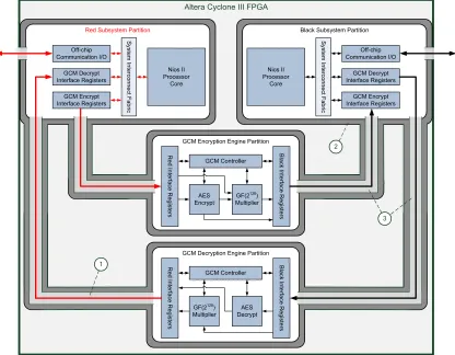
Altera Cyclone III FPGA
Red Subsystem Partition
Nios II Processor Core S ys te m In te rc on ne ct F ab ric Off-chip Communication I/O GCM Encrypt Interface Registers GCM Decrypt Interface Registers
GCM Encryption Engine Partition
AES Encrypt
GF(2128)
Multiplier GCM Controller B la ck In te rfa ce R eg is te rs R ed In te rfa ce R eg is te rs
GCM Decryption Engine Partition
GF(2128)
Multiplier AES Decrypt GCM Controller B la ck In te rfa ce R eg is te rs R ed In te rfa ce R eg is te rs
Black Subsystem Partition
[image:10.612.105.521.92.416.2]Nios II Processor Core S ys te m In te rc on ne ct F ab ric Off-chip Communication I/O GCM Encrypt Interface Registers GCM Decrypt Interface Registers 2 1 3
Figure 1.1: Dataflow diagram of FPGA-based, multi-processor HW-SW system with AES GCM encryption and decryption engines.
1) SRI connecting two secured regions
2) a fence of unused logic around a secured partition
3) two SRIs containing signals relating only to the encrypted data
The Nios II processor itself has many features that can be added or removed based on need [1]. This feature set will be one of the variables in the test platform. For example, the performance benefits of adding caching could be weighed against the area requirement on the entire test platform.
The target FPGA for this project will be an Altera Cyclone III EP3C120F780C7N. Thus the tools for physical separation of FPGA logic will be provided by Altera’s Quartus II software [2]. This particular FPGA does not offer the same physical security protections available in the Cyclone III LS series FPGA, but will allow testing of the correctness of the designed system’s output.
The crypto-engine will be an implementation of the Advanced Encryption Standard, see section 2.2. AES is the most applicable block cipher candidate to use in such a system because it has been approved by the government for use in securing classified material [3]. A thorough analysis of several different AES implementations will be performed. At a high-level, the AES implementations will vary architecturally. Targeted architectures will include intuitive round iterative designs, as well as unrolled designs for higher performance. The operating mode will target GCM for high performance and authentication.
The key length will be varied between 128 and 256 bits. Increasing concern has been expressed over the strength of the larger bit variants of AES, particularly in the key schedule [4]. This thesis will provide comparisons of performance and FPGA reconfigurable logic usage (area) between the two key sizes. A designer could use this information to make an informed decision in favor of a particular implementation. Such a decision could be reached by comparing the potential increase in security with a larger key length versus the increase in utilized FPGA area or impact to throughput.
implementation to increase throughput [5]. These designs will be analyzed in conjunction with high-level architectural strategies.
2. Essential Background
This introductory chapter elucidates the major background topics involved in this thesis. A description of general block ciphers is given. The focus is then narrowed to AES. Several modes of operation of block ciphers are described for completeness. The pertinent features of modern FPGA devices are described along with two different softcore processors.
2.1
Block Cipher Algorithms
A block cipher is an algorithm that accepts data input of a fixed n-bit length and, with the addition of a secret k-bit key value, produces n-bits of encrypted output based on the two inputs. The block cipher’s encryption algorithm is paired with a decryption algorithm that, when using the identicalk-bit key value, can reproduce the original data input. The
n-bit length defines the block size of the cipher. A block cipher is known as a symmetric key algorithm because it requires the same key for decryption that was used during the encryption process.
The data input to this cipher, known as plaintext, can be any type of information that can be represented in the form of a binary string of data. The manner in which the plaintext is presented to a block cipher is defined by the operational mode in which the cipher is used. These modes of operation [6, 7, 8, 9] are necessary for improved security or per-formance when the amount of plaintext is larger than the size of a single block [10]. This encrypted output of a block cipher is known as ciphertext. Equation 2.1 and Equation 2.4 illustrate the invertible nature of the encryption and decryption functions, labeledEk and
Ek(P) = C (2.1)
Ek−1(Ek(P)) = Ek−1(C) (2.2)
P = Ek−1(C) (2.3)
P = Dk(C) (2.4)
Underlying component algorithms in block ciphers make use of well-known mathe-matical principals. The focus of this work, the Advanced Encryption Standard [12], is composed of both linear and non-linear functions that serve to make the ciphertext unintel-ligible to anyone without possession of the key. The regularity in the structure comes from component pieces that are iterated over multiple times in one encryption or decryption op-eration. Due to the symmetric nature of AES, the component pieces can often be reused between encryption and decryption.
2.2
Advanced Encryption Standard
In the early 1970s, the National Bureau of Standards (NBS), soon to be called the National Institute of Standards and Technology (NIST), found a growing need for a government standard for securing sensitive documents. After two rounds of proposal submissions, a candidate from IBM, was selected as the winning algorithm in November of 1976. This winning algorithm is a direct descendant of IBM’s Lucifer cipher [13].
The winning algorithm from IBM became known as the Data Encryption Standard (DES) and there have been several reaffirmations of it to date [14]. In each of the doc-uments, the block cipher is referred to as the Data Encryption Algorithm (DEA). For the remainder of this thesis document, the initialisms DEA and DES will be used interchange-ably to refer to the block cipher algorithm proposed by the Federal Information Processing Standard (FIPS) publication [14].
force search of the DES keyspace, NIST began a second competition for a standard block cipher algorithm on January 2, 1997 [13]. Moreover, NIST specified the algorithm should be “as secure as triple-DES, but much more efficient” [15]. In this competition the algo-rithm’s block size was required to be 128bits and was required to support keys of lengths
128, 192, and 256 bits. Of the five final round candidates, Rijndael was noted as having the best balance of security, performance, efficiency, implementability and flexibility. For these reasons, NIST adopted Rijndael as the Advanced Encryption Standard on November 26, 2001 [12]. Several changes were made to the original algorithm, such as fixed block sizes instead of variable block sizes, before it was approved as a standard [13]. AES is the first public algorithm approved for use in systems intended to protect classified data [3].
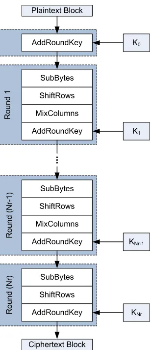
AES is an iterated, product cipher that maintains an internal 128 bit state. The inter-nal state is initialized to the value of the plaintext block before being added to the initial round key. During a round of AES, there are three key independent operations, also called transformations, performed before the round key is added to the internal state. These round operations are SubBytes, ShiftRows, MixColumns and AddRoundKey. The number of it-erations of the round opit-erations is dependent upon the length of the key. As in [12], N r
will be used to represent the number of rounds andN kwill be used to represent the number of32bit words in the input key. WhenN ris10,12, or14, N k is4, 6, or8, respectively. The input key is expanded into N r round keys, also called subkeys. The general round structure of AES is shown in Figure 2.1.
Both the plaintext input to the algorithm and the internal state size are 128 bits, or 4 32-bit words. [12] states thatN b is the number of column words in the state. Since this value is fixed by the specification,N bwill always be4words.
2.2.1
SubBytes
AddRoundKey
ShiftRows SubBytes
MixColumns AddRoundKey
ShiftRows SubBytes
AddRoundKey Plaintext Block
Ciphertext Block
R
ou
nd
1
R
ou
nd
(
N
r)
ShiftRows SubBytes
MixColumns AddRoundKey
R
ou
nd
(
N
r-1)
K0
K1
KNr-1
[image:16.612.239.394.96.452.2]KNr
Figure 2.1: The general round structure of AES.
several possible inter-round optimizations. SubBytes operates by independently exchang-ing each byte of the internal state with a value from a substitution box, shown in figure Figure 2.2. SubBytes does not have any output bytes that are equivalent to the original input to the round operation, which implies it is a derangement.
While the act of substituting values in the state a byte at a time is somewhat simple in concept, the derivation of the substitution box values is more complicated. SubBytes consists of two major operations, each with its own particular design criteria. The first operation on the state byte is the calculation of its inverse in GF(28), labeledG, followed by
S'0,0S'0,1S'0,2S'0,3
S'1,0S'1,1 S'1,3
S'2,0S'2,1S'2,2S'2,3
S'3,0S'3,1S'3,2S'3,3 S0,0 S0,1 S0,2 S0,3
S1,0 S1,1 S1,2 S1,3
S2,0 S2,1 S2,2 S2,3
S3,0 S3,1 S3,2 S3,3
S-Box
[image:17.612.177.445.89.189.2]S1,2 S'1,2
Figure 2.2: SubBytes effect on the internal state [12]
performed by the SubBytes round.
Sbox[a] =A(G(a)) (2.5)
The calculation of the inverse is the origination of the algorithm’s nonlinearity. Accord-ing to [15], two important design criteria for the non-linear stage operation are that it has a small maximum input to output correlation and a small difference propagation probability. These are two factors that have an impact on the linear and differential cryptanalysis of the algorithm. The affine transform gives the sbox some algebraic complexity within GF(28)
[15].
The affine transform is define as the resultant bit a0i over GF(2) fori ∈ {0,1, . . . ,7}
with input bitaias:
a0i =ai⊕a(i+4) mod 8⊕a(i+5) mod 8⊕a(i+6) mod 8⊕a(i+7) mod 8⊕ci (2.6)
Theci constant value used in Equation 2.6 is defined as theithbit of a constant byte6316.
This bitwise equation is a linear transformation followed by a translation by the constant bit. This relationship can also be expressed as a matrix multiplication and the binary addition of the constant 6316 expressed as a binary matrix [12]. Equation 2.7 shows the affine
a0i =σ×ai⊕ci
a07
a06
a05
a04
a03
a02
a01
a00 =
1 1 1 1 1 0 0 0 0 1 1 1 1 1 0 0 0 0 1 1 1 1 1 0 0 0 0 1 1 1 1 1 1 0 0 0 1 1 1 1 1 1 0 0 0 1 1 1 1 1 1 0 0 0 1 1 1 1 1 1 0 0 0 1
× a7 a6 a5 a4 a3 a2 a1 a0 ⊕ 0 1 1 0 0 0 1 1 (2.7)
Even though the derivation of the substitution box values is more complicated than a simple look up table, certain implementation techniques can be exploited that result in a design with higher throughput. The calculations for the hardware Galois field inversion can be found in chapter 4.
The inverse SubBytes round applies the inverse of the two intra-round operations. The finite field inversion is its own inverse, so no changes need be applied to its internal al-gorithm. The affine transform, however, must be inverted. The two operation must be applied in the opposite order from the forward SubBytes round operation, as illustrated in Equation 2.8.
a0i =σ−1×ai⊕c−i1
a07
a06
a05
a04
a03
a02
a01
a00 =
0 1 0 1 0 0 1 0 0 0 1 0 1 0 0 1 1 0 0 1 0 1 0 0 0 1 0 0 1 0 1 0 0 0 1 0 0 1 0 1 1 0 0 1 0 0 1 0 0 1 0 0 1 0 0 1 1 0 1 0 0 1 0 0
× a7 a6 a5 a4 a3 a2 a1 a0 ⊕ 0 0 0 0 0 1 0 1 (2.9)
2.2.2
ShiftRows
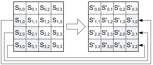
The ShiftRows round operation cyclically shifts each row in the state matrix by a constant offset. The offset by which each row is shifted is unique to each row. This was a design requirement defined in [15] to provide resistance against linear and differential cryptanaly-sis. The shift offsets are equal to the row index when the rows indices begin at 0. The first row is shifted by zero bytes, the second row by one byte, and so on. Figure 2.3 illustrates the ShiftRows operation.
S2,3
S'1,3 S'0,0S'0,1S'0,2S'0,3
S'1,1S'1,2 S'1,0
S'2,2S'2,3S'2,0S'2,1
S'3,3S'3,0S'3,1S'3,2 S0,0 S0,1 S0,2 S0,3
S1,0 S1,1 S1,2 S1,3
S2,0 S2,1 S2,2
[image:19.612.178.443.482.595.2]S3,0 S3,1 S3,2 S3,3
Figure 2.3: The state matrix on the left is transformed by the ShiftRows operation to be the matrix shown on the right.
operations. The shift offsets are also equivalent.
2.2.3
MixColumns
The MixColumns round operation is the only round operation where high performance is not trivial to obtain [15]. An important design criterion for this stage was having the internal state columns be exactly four bytes. This was done in order to increase performance via look up tables on 32 bit architectures. Two other design criteria, linearity over GF(2) and relevant diffusion, were added to in response to the criteria for the wide trail design strategy [15].
During this round, each column in the state matrix is multiplied by another fixed poly-nomial modulox4+ 1. This operation is accomplished by first creating a polynomial with
coefficients that are the bytes in the current column in the state matrix. More about this representation can be found in section 3.1. This column polynomial is multiplied by the fixed polynomial, labeledc(x), shown below:
c(x) = 0316x3+0116x2+0116x+0216 (2.10)
This operation can be represented as a matrix multiplication, shown in Figure 2.4.
S2,3
S'1,3 S'0,0S'0,1S'0,2S'0,3
S'1,1S'1,2 S'1,0
S'2,2S'2,3S'2,0S'2,1
S'3,3S'3,0S'3,1S'3,2 S0,0 S0,1 S0,2 S0,3
S1,0 S1,1 S1,2 S1,3
S2,0 S2,1 S2,2
S3,0 S3,1 S3,2 S3,3
[image:20.612.166.454.481.656.2]02 01 01 03 03 02 01 01 01 03 02 01 01 01 03 02 j i j i j i j i S S S S , 3 , 2 , 1 ,
×
The inverse mix columns operation follows the same order of operations as mix columns, however the constant polynomial is inverted. The polynomial in Equation 2.10 is relatively prime to the modulusx4+ 1, thus it is invertible. This inverted equation is shown below in
Equation 2.11.
c−1(x) = 0B16x3+0D16x2+0916x+0E16 (2.11)
2.2.4
AddRoundKey
The AddRoundKey (ARK) round performs a bitwise XOR with each byte of the current round key and each byte of the state. This operation is illustrated in Figure 2.5. The round keys have the same structure as the internal state. The round keys are taken from the ex-panded key. The procedure to generate the exex-panded key is known as the key schedule and will be detailed in subsection 2.2.5. AddRoundKey and its inverse are the same operation.
S2,3
S'1,2 S'0,0S'0,1S'0,2S'0,3
S'1,0S'1,1 S'1,3
S'2,0S'2,1S'2,2S'2,3
S'3,0S'3,1S'3,2S'3,3 S0,0 S0,1 S0,2 S0,3
S1,0 S1,1 S1,2 S1,3
S2,0 S2,1 S2,2
S3,0 S3,1 S3,2 S3,3
K2,3 K0,0 K0,1 K0,2 K0,3
K1,0 K1,1 K1,2 K1,3
K2,0 K2,1 K2,2
K3,0 K3,1 K3,2 K3,3
[image:21.612.141.478.388.479.2]=
Figure 2.5: ARK operates by performing a bitwise XOR between each byte of the state and the generated round keys [15].
2.2.5
Key Schedule
During every ARK round, the current state is combined with a round key through a bitwise XOR operation. This round key is a four word part of an expanded key derived from the original private key. The size of the key controls the number of rounds, which increases the number of total ARK rounds, which each need a round key. The number of round keys is
After the initial private key is used, N r round keys are generated. The round keys are generated sequentially by words. If a count is kept for every word generated, each generated word is an XOR between the previous word and the wordN bbefore the current word, which is the previous round word at the same position as the current word. Additional operations are required for every word that has a count equal to a multiple of N k. In that case, instead of using the previous word directly in the bitwise exclusive OR (XOR) operation, the previous word is first processed by RotWord, SubWord, and then XORed with a round constant. The key schedule128bit input key,N k = 4, is shown in Figure 2.6. IfN k = 8, then there is one more additional step. Whenever the word count is equivalent to4 mod 8, the previous word will first be processed by the SubWord operation [12]. This is shown in Figure 2.7.
The SubWord step performs the SubBytes operation from the AES encryption algo-rithm on each byte in the current word. The RotWord step cyclically rotates the current word, shown in Equation 2.12.
[a1, a2, a3, a4]⇒[a2, a3, a4, a1] (2.12)
The round constants are hexadecimal 00, 01, 02, 04, 08, 10, 20, 40, 80, 1B, and 36. Three bytes of zeros are appended to each of these round constants to make each the length of an entire word. The constants are derived from repeated squaring of an indeterminatexin GF(28)[15].
+ +
+ + RotWord
SubWord
+ Rcon[1]
W0
W1
W2
W3
Private Key W0 W1 W2 W3
K0
K1
+ +
+ + RotWord
SubWord
+ Rcon[10]
K10
W0
W1
W2
W3
W0
W1
W2
W3
... ... ... ... ...
[image:23.612.142.468.211.539.2]Expanded Key
+ +
+ +
Private Key
W0 W1 W2 W3
K0
K1
Expanded Key
W4 W5
+ + K2
K3
W6 W7
+ +
+ +
+ +
+ + K13
K14 + +
SubWord RotWord
SubWord
+ Rcon[1]
··
·
··
·
··
·
··
·
··
·
··
·
··
·
··
·
··
·
SubWord RotWord
SubWord
[image:24.612.142.468.169.578.2]+ Rcon[7]
2.2.6
Decryption
The straight forward decryption algorithm can be created by applying the inverse round operations in the opposite order that they were originally applied. The round keys used during the AddRoundKey round must also be applied in the opposite order they were during encryption. This implies that the key schedule must process all of the round keys before the first round of decryption can begin. Since each round key depends on the generation of the previous, each round key much first be generated before the final round key can exist.
It is possible to create a key schedule that generates the decryption keys in the order that they are needed. Such an algorithm would need the final N k words from the round keys generated during encryption [15]. Use of inverse key generation implies a dependence on forward key generation being performed at some point where these final round key words would be made available.
Due to the commutative nature of the InvSubBytes and InvShiftRows round operations, their order can be reversed. The InvMixColumns round operations are linear with respect to the column input, which allows the operation shown in Equation 2.13 from [12].
InvMixColumns((state)⊕(round key)) =
InvMixColumns(state)⊕InvMixColumns(round key)
(2.13)
Using the linear properties of the different rounds, an equivalent inverse cipher can be created. These two inversion algorithms are shown in Figure 2.8 for a 128bit private key. The equivalent inverse has the advantage of performing the rounds in the same order as their counterparts in the encryption algorithm. This has the advantage of allowing certain hardware structures to be reused between the two algorithms.
R ou nd 1 0 R ou nd 9 R ou nd 1 AddRoundKey InvSubBytes InvShiftRows AddRoundKey InvMixColumns InvSubBytes InvShiftRows AddRoundKey K10 Ciphertext K9 K0 Plaintext R ou nd 1 R ou nd 1 0 InvSubBytes InvShiftRows AddRoundKey
InvMixColumns K1
R ou nd 9 AddRoundKey InvShiftRows InvSubBytes InvMixColumns AddRoundKey InvShiftRows InvSubBytes AddRoundKey K10 K0 Plaintext InvShiftRows InvSubBytes InvMixColumns AddRoundKey
InvMixColumns K9
K1
[image:26.612.109.521.93.447.2]InvMixColumns Ciphertext
Figure 2.8: The diagram on the left shows the straight forward inverse cipher algorithm, while the one on the right shows the equivalent inverse cipher for a128bit key [12]. these operating modes include certain feedback modes or in the generation of a message authentication code [17].
2.3
Block Cipher Modes of Operation
in this section. More specific information can be found in the NIST special publications [6, 7, 8, 9].
2.3.1
Confidentiality Modes
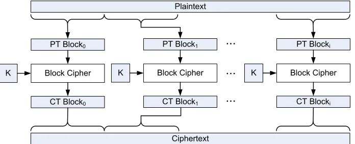
The most straightforward operating mode is Electronic Codebook (ECB) Mode. In ECB, a message is divided into blocks that have the same length as the fixed block cipher input. Each of these message blocks are encrypted individually, as shown in Figure 2.9. A weak-ness in this operational mode presents itself when a duplicate block is encrypted. Such a block would encrypt to the same ciphertext when used with an identical key, allowing an attacker to derive some information about the encryption. An example of this weakness is illustrated in Figure 2.10 where the output clearly reveals information about the original image. One positive benefit of this mode of encryption is that an error during encryption of one block will result in an error in only one ciphertext block [11].
PT Block0
Block Cipher K
Plaintext
PT Block1 ∙∙∙ PT Blocki
Ciphertext
CT Block0 CT Block1 CT Blocki
Block Cipher ∙∙∙ Block Cipher
∙∙∙
K K
Figure 2.9: An example of encryption using a block cipher in ECB mode.
Figure 2.10: The figure on the left [18] is encrypted using a block cipher in ECB, resulting in the figure on the right [19].
to the dependency on the previous ciphertext block, none of the ciphertext blocks can be computed in parallel. Decryption, however, can be computed in parallel since the cipher-text blocks are readily available. CBC is self-synchronizing, meaning that any errors in the current operation will affect the current result and the result of the next operation, but not the third result [6].
PT Block0
Block Cipher K
Plaintext
PT Block1 PT Blocki
∙∙∙
Ciphertext
CT Block0 CT Block1 CT Blocki
Block Cipher Block Cipher ∙∙∙
∙∙∙
K K
+ +
[image:28.612.173.451.89.242.2]IV +
Figure 2.11: An example of encryption using a block cipher in CBC mode.
cipher’s block size. In these key stream generating ciphers, padding is not necessary. OFB maintains an internal state by repeatedly encrypting an IV. The output from each of these encryptions is then exclusively-ORed with the plaintext, producing a block of cipher text. During the final decryption, bits generated from the block cipher that are in excess of the size remaining plaintext are discarded [6].
Counter mode operates in similar fashion to OFB. Counter mode generates its keystream by encrypting a counter or predictable sequence [15]. Unlike OFB, counter mode can cal-culate ciphertext blocks in parallel since the input to the block cipher is not dependent upon a sequentially encrypted IV.
CFB has a similar structure to OFB, except that the sequentially generated ciphertext is input to the next block cipher instead of a continuous encrypted IV. The CFB structure is illustrated in Figure 2.12 wheresbits of plaintext are exclusive-ORed withbbits of block cipher output for 1 ≤ s ≤ b. For each XOR operation, b −s bits of the block cipher output are discarded. The input into each block cipher must be a multiple of its block size
b, so thescipher text bits are appended to the least significantb−sbits from the previous block cipher input [6]. CFB has an advantage over counter mode and OFB in that it is self-synchronizing, like CBC [15]. This self-synchronizing property of OFB assures that it will recover from an error after bs blocks of ciphertext [6].
PT0 (s bits)
Plaintext
PT1 (s bits) PTi (s bits)
Ciphertext
CT0 (s bits) CT1 (s bits) CTi (s bits)
∙∙∙
+ +
IV Block Cipher +
K
Block Cipher K
Block Cipher K ∙∙∙
[image:29.612.102.525.486.618.2]∙∙∙
2.3.2
Authentication Mode
The nature of a message authentication code (MAC) is to ensure the integrity of a data by verifying its authenticity. A block cipher can be used to generate a secure MAC when the algorithm is generally accepted as being secure. CBC-MAC was originally designed for this purpose, but was replaced by Cipher-based Message Authentication Code (CMAC) to allow for message lengths that are not fixed as a multiple of the block size [7, 11].
CBC-MAC operates by using a block cipher in CBC mode, as described in subsec-tion 2.3.1, then use the last bits of ciphertext as the MAC [15]. CMAC is a variasubsec-tion of the CBC-MAC algorithm. CMAC generates two subkeysK1andK2from a given private key
K, which both have a length equal to the block size of the cipher. This private key is used to encrypt complete message blocks, following the CBC algorithm, until the last block is reached. If this last block is equal to a block length, it is masked with subkey K1. If the last piece of the message is not equal to the block size, the binary sequence 100. . .0is appended to the message before being masked with subkeyK2. This masked value is then encrypted once more with the keyK. The most significant bits on the output of this cipher are used as the CMAC [7].
2.3.3
Authenticated Encryption Modes
Galois/Counter mode (GCM) provides the same encryption and authentication options as CCM, but is parallelizable and relatively efficient [9]. As specified in [8] and [9], GCM and CCM must use an NIST approved block cipher with a block size of 128 bits. The GCM proposal [20] had originally made allowances for block ciphers with both 128 and 64 bit block sizes. Like CCM, GCM operates on a packet of data consisting of Additional Authenticated Data (AAD) and plaintext. AAD is information that does not need to be encrypted, but can be validated with the generated tag value.
The confidentiality within GCM originates with the block cipher counter mode of oper-ation. This operation is illustrated in Figure 2.13. The initial counter block (ICB) is, quite literally, the first value of the counter to be encrypted. Since counter mode generates a key stream, only the most significant bits of the final encrypted counter block are needed in the plaintext XOR if the final plaintext block is not equal to the block size [9].
Block Cipher K
+
CT1
inc32
PT1
ICB
Block Cipher K
+
CT2
PT2
CB2
Block Cipher K
+
CTi
PTi
CBi
MSBlen(PTi)
Figure 2.13: The GCTR function where the inputs, the ICB, key and plaintext PTi, are
shown in light blue, and the ciphertext CTi, is shown in dark blue [9].
To provide authentication, GCM makes use of a GHASH function. This function, show in Figure 2.14, employs a hash subkey, depicted as H. H is generated by encrypting a complete block of all zeroes with the private keyKused throughout the algorithm. GHASH multiplies the current input block Xi with ciphertextH in GF(2128) modulox128 +x7 +
x2 +x+ 1, effectively evaluating the Equation 2.14 from [9]. The degree of the reduction
with the final input block.
X1·Hi⊕X2·Hi−1⊕. . .⊕Xi−1·H2⊕Xi·H1 (2.14)
Y1
X1
Y2
X2
Yi
Xi
+ +
[image:32.612.208.406.145.312.2]∙ H ∙ H ∙ H
Figure 2.14: The GHASH function with inputsXiand final output hashYi[9].
Before the IV can be used in GCM, it must first be processed by the pre-counter block
J0. During this stage, processing occurs on the IV to ensure it is 128bits in length before
it is used in the GCTR function. Figure 2.15 shows how the IV, plaintext, AAD, and key inputs are used to produce both the tag and the ciphertext. As described earlier, the GHASH function operates on block size input. The AAD and ciphertext are padded with enough zeroes to guarantee each is a multiple of the block size. Additionally, the AAD and ciphertext lengths are specified are 64 bit representations. Their total bit field length is 128bits, the block size. The hashed value of the AAD, ciphertext, and their respective lengths is encrypted with the GCTR function using the original value fromJ0and the most
significanttbits are used as the tag. [9] has specific recommendations for the length of the tag based on the purpose of its use.
Plaintext
Tag
GCTR K
CT 0u
AAD 0v Len(AAD) Len(CT)
J0
IV
inc32
GHASH
GCTR
MSBlen(Tag)
Block Cipher 0128
m∙128 bits n∙128 bits 64 bits 64 bits
[image:33.612.132.486.87.337.2]H
Figure 2.15: The operations in GCM from the IV, plaintext, AAD, and key inputs, shown in light blue, to the tag and ciphertext outputs, shown in dark blue [9].
[9].
2.4
Field Programmable Gate Arrays
In order to fully understand the purpose of FPGAs, it is important to understand the dif-ferences in the design development process for a general purpose processor and for an Application Specific Integrated Circuit (ASIC). A general purpose processor is an inte-grated circuit that is designed with hardware implementing a variety of common logical operations. The processor executes a series of instructions that dictate how it will oper-ate. The instructions are readily programmed into the device. More complex processors offer varying degrees of instruction level parallelism or hardware support for more logical functions, floating point arithmetic units for example.
of accomplishing a specific task. A full custom designed ASIC is engineered from individ-ual transistors. This implies a considerable amount of time and resources be allocated for development of more complex systems. Using standard cells reduces the amount of design time by providing the engineer with a variety of logic having a high density and known electrical properties. Often a standard-cell ASIC is designed using a hardware descrip-tion language. A structured ASIC offers the same benefits to design time as standard-cell ASICs. Unlike standard-cell ASICs, a structured ASIC makes use of predefined metal layers. This has the effect of reducing manufacturing time as well.
An FPGA is intended to be a convenient middle ground between an ASIC and a general purpose processor. The hardware realization time for an ASIC is much greater than that of an FPGA and it can be more costly to develop. An FPGA combines the flexibility and programming speed of a general purpose processor with high performance found in custom designed hardware units. Modern FPGAs have the ability to implement a general purpose processor utilizing the available FPGA logic structures. These are known as soft proces-sor cores or softcore procesproces-sors, since the procesproces-sor utilizes the FPGA’s programmable resources for its construction. This allows for hardware/software co-design within a single FPGA chip.
In contrast to softcore processors, Xilinx has incorporated one or more physical Pow-erPC cores within the fabric of certain model FPGAs. These physical processor cores support higher clock rates and provide better performance than the softcore processor al-ternatives. Like softcore processors, a physically embedded processor can take advantage of any custom designed hardware units that are present and have been routed to it. Unlike softcore processors, the physically embedded processor is limited to the feature set present during the FPGA’s construction.
variety of applications for over 20 years.
[image:35.612.151.468.401.624.2]An FPGA is made up of a matrix of reconfigurable logical blocks built on a fabric of interconnections. These blocks vary in their composition between device manufacturers and models. Xilinx refers to the reconfigurable blocks as configurable logic blocks (CLBs), while Altera names them logic array blocks (LABs). The structure and routing interconnec-tions of an Altera Cyclone III LAB is shown in Figure 2.16. The terminology describing the structures within an FPGA often differs between manufacturers, but the components it refers to are typically very similar. Within the reconfigurable blocks are smaller units, known as slices (Xilinx) or logic elements (Altera), which commonly contain a lookup table (LUT), configurable multiplexors, and registers [22, 23]. Figure 2.17 illustrates the structure of a logic element (LE) in an Altera Cyclone III. The smallest design unit address-able by the device programming tool defines the FPGA’s granularity [5]. Fine granularity allows for easier manipulation of individual bits, while a course granularity allow for better manipulation of high-level logical structures.
Figure 2.16: The structure of a logic array block in an Altera Cyclone III device [23].
Figure 2.17: A logic element in an Altera Cyclone III device [23].
span the length of the chip and are typically used for global signal routing. Logic elements in Altera FPGAs are connected via a direct local interconnect, which helps to minimize the amount of row and column interconnects between LABs. Xilinx FPGAs use hex and double interconnects to connect large groups of CLBs via a Global Switch Matrix (GSM) [24]. More recent FPGAs offer even more types of routing that can provide increased performance [5].
In the Xilinx Virtex series and Altera Cyclone series FPGAs, there are at least two types of on-chip memory available. Both FPGAs offer distributed RAM created by the LUTs within the respective FPGA’s primitive reconfigurable elements. The other common type of memory is block random access memory (BRAM). BRAM is located in columns throughout the FPGA and varies in size based on the model of the FPGA. The distributed RAM is designed to store smaller amounts of data, while BRAM has a configurable width and depth for creating larger memory blocks [5].
(a) Nios II [1] (b) MicroBlaze [25]
Figure 2.18: High level layouts of Altera’s Nios softcore processor (2.18a) and Xilinx’s MicroBlaze softcore processor (2.18b).
3. Mathematical Background
This chapter presents the basic properties of a group, developing into properties of a ring, then into properties of a finite field. An overview will be presented of several finite field representations, along with their associated field arithmetic. Implementation techniques discussed in later chapters require manipulation of binary data in composite finite fields. With that in mind, composite field mathematics and the isomorphic mappings between composite field representation and standard binary representation will be discussed. It is assumed the reader has an understanding of some general number theoretical concepts.
3.1
Finite Fields
The majority of the calculations performed in AES are over a finite field. To that end, an effort is made to explain preliminary and related concepts. The topic of finite fields is expanded upon in great detail in books [26] and [27]. Detailed descriptions of composite fields and the isomorphic mappings to and from composite fields can be found in Paar’s doctoral thesis [28] and in the master’s thesis of his student, Jorge Guajardo [29].
3.1.1
Preliminary Concepts
In order to define a finite field, it is necessary to define some terminology and basic con-cepts.
Definition 1 [26] A binary operationon a set S is one that maps the Cartesian product,
S×S, of two elements fromSback on to the setS.
Definition 2 [26, 28] A setG, defined with a binary operation, is called agroupif it obeys
• Associativityof the binary operation: (ab)c=a(bc),∀a, b, c∈G • Identity elemente∈G:ae =ea =a
• Inverse elementa−1 ∈Gfor any elementa ∈G: aa−1 =a−1a=e
• Gis not the empty set
A group is described as beingabelian, or commutative, ifab=ba,∀a, b∈G.
Similar to the concept of a group is a ring. Unlike a group, a ring is defined with two binary operations. It is important to note that there is no requirement for a well defined multiplicative inverse for every element in a ring.
Definition 3 [26] A setR, defined with two binary operations: addition(+) and multiplication(·),
is called aring1if it obeys the following properties:
• Associativitywith respect to each binary operation:
(ab)c=a(bc)anda+ (b+c) = (a+b) +c,∀a, b, c∈R
• Ris anabelian group under additionwith identity element0
• Additive Inverse elementb∈Rfor any elementa∈R:a+b =b+a = 0
• Identity elementfor multiplication1∈R:1·a=a·1 =a,∀a∈R • Distributivity∀a, b, c∈R: a(b+c) =ab+ac= (b+c)a
• Ris not the empty set
Using the definition of a ring, a field can be defined with some additional properties.
Definition 4 [26] A ringRforms afieldif it obeys the following properties:
• The nonzero elements ofRform anabelian group under multiplication
• Multiplicative identity element1is not equal to the additive identity element0
Every field is an integral domain [26], which specifies that the field has no zero divisors. This is especially useful along with the definition of the division operation. That then implies there exists a multiplicative inverse for every element in the field.
1[26] calls this a “ring with identity”, since it has a multiplicative identity element. Either notation is
For the work performed in this thesis, only finite fields are of relevance. A finite field is a field with finitely many elements, also known as a Galois field. A Galois field is abbreviated as GF(pn) or
Fpn, where n is positive integer and p is a prime number. pn
indicates the order of the field, whilepindicates the characteristic of the field [27].
Definition 5 [28] Theorderof a field is the number of elements in the field.
Definition 6 [28] Thecharacteristicof a field is number of additions of the multiplicative
identity element necessary to reach a sum equivalent to the additive identity element.
In addition to the restriction of focus in this thesis to Galois fields, these finite fields will also be restricted to a characteristic of two. As was stated in [28], every element will be its own additive inverse. The motivating factor here is to create a field that can easily be represented by the Boolean equations that define the operation of digital logic.
3.1.2
Finite Fields Extensions
A ring of integers is denoted Zn, where n is the integer modulus. In similar fashion, a
ring of polynomials can be created modulo a polynomial f(x). This ring of polynomials is denoted Zn[x]
f(x), wheref(x) ∈Zn[x]. The ring of integersZnbecomes a finite field when n is prime. When applying the same logic to the ring of polynomials, one must conclude that, not only would n have to be prime, the polynomial modulus f(x)would have to be irreducible for Zn[x]
f(x) to be a field [29]. These irreducible polynomials exist for every finite
field with order being of a prime power.
Theorem 1 [27, 26] If a fieldF exists and contains a number of elements equal to a power
of a prime, then∀d ≥ 1, there is at least one irreducible polynomial of degreedover the
fieldF.
The previous subsection defined GF(pn)as a Galois field with its modulus being of a
is known as an extension field of GF(p). Conversely, GF(p)is a subfield, or ground field, of GF(pn). An element in the extension field GF(pn)can be represented as a polynomial
with coefficients in the subfield. For example, a polynomial A(x) = an−1xn−1+. . .+a0
has coefficientsai ∈GF(p), wherenis the maximum degree of the irreducible polynomial
f(x)andi= 0,1, . . . , n−1[29]. The maximum degree of the indeterminatexwill never be greater thann−1, since it is reduced by the irreducible polynomialf(x)with degreen. Thepnpolynomials are the residue classes modulof(x)in GF(pn), which implies that the algorithms for arithmetic in the field will depend on the choice off(x)[28].
Composite Fields
A special case of extension fields are composite fields, denoted as GF((2n)m)for a
charac-teristic of two.
Definition 7 [28, 29] A pair of fields{GF(2n), Q(y) =yn+Pn−1
i=0 qiyi}and
{GF((2n)m), P(x) = xm+Pm−1
i=0 pix
i}are called acomposite fieldif. . .
• GF(2n)is constructed from GF(2)byQ(y)
• GF((2n)m)is constructed from GF(2n)byP(x)
, whereQ(y)andP(x)are irreducible polynomials over GF(2)
If k = nm, GF(2k) and GF((2n)m) have the same order. Any two fields with the
3.1.3
Basis and Representation
Although there are many different basis representations, three are commonly found in ap-plied cryptography research: the standard basis, the normal basis, and the dual basis. The selection of a particular basis representation determines the complexity of the finite field arithmetic and any constructed isomorphisms. Field element representations will be shown and an overview will be given for each of the three bases. Specific details regarding basis representation can be found in [26, 30] with implementations described in chapter 4.
A basis for a finite field is a set of elements that, when linearly combined, form every element within the finite field. A general basis for GF(pm) is shown in Equation 3.1, whereairepresents a coefficient,xirepresents a basis vector, andA(x)is an element in the
finite field. The number of basis elementsm is directly related power of the prime integer defining the ground field.
A(x) = a0x0+a1x1+a2x2+. . .+am−1xm−1, whereai ∈GF(q) (3.1)
Standard Basis
If a finite field extension GF(2R(mx)[)x]is formed over GF(2), the standard basis for the extension over the ground field GF(2) is shown in Equation 3.2 using the root x of R(x). This primitive rootxis known as the generator.
{1, x, x2, . . . , xm−1} (3.2)
Each vector within this basis is linearly independent of every other basis. The melements within the field GF(2m)are represented as polynomials of the form shown in Equation 3.3.
Eachai is an element of the ground field GF(2). As with any basis, a linear combination
of thembasis elements produces each of the finite field elements [28].
The standard basis is also known as the polynomial basis or canonical basis, specifically with regards to finite field extensions. The origin of the polynomial basis name is obvious because of the direct connection between the basis and element representation as a polyno-mial [28]. Finite field arithmetic operations using the standard basis are performed modulo a field reduction polynomial, as was mentioned in subsection 3.1.2. Each coefficient of the indeterminate in field element representation is also reduced by the modulus of the ground field.
Using a field of characteristic two, addition is equivalent to subtraction. This is a sim-ple exclusive-OR operation with the coefficients at equivalent powers of the indeterminate. Multiplication and squaring are more complex operations with a variety of different im-plementations with specific advantages. Multiplication in the standard basis, in its most elementary form, is performed using the same methods as conventional polynomial multi-plication. The exception is in the reduction steps described in the previous paragraph. A squaring operation involves some shifting operations followed by a multiplication and an exclusive-OR operation.
Normal Basis
If the same finite field extension GF(2R(mx)[)x] is formed over GF(2), as in section 3.1.3, the normal basis for the extension field over the ground field GF(2)is shown in Equation 3.4.
{x, xq, xq2
, xq3, . . . , xqm−1} (3.4)
A(x) =a0x+a1x2 1
+a2x2 2
+. . .+am−1x2 m−1
, whereai ∈GF(q) (3.5)
Like the standard basis, addition in the normal basis is a simple exclusive-OR of the respective primitive element’s coefficients. Unlike the standard basis, multiplication is more complex. An advantage of the normal basis is that squaring is a simple cyclic shift of the primitive elements coefficients.
Dual Basis
In the standard basis, elements were of successive generator powers. In the normal basis, elements were of successive generator exponentiations. A dual basis can be created for any basis [30, 28]. Using the basis elements {x0, x1, . . . , xm−1} of GF(qm)from the generic
example in subsection 3.1.3, let h be a nonzero linear function from GF(qm) to GF(q). Using this basis, its dual basis can be defined as{γ0, γ1, . . . γm−1}, where
h(xiγi) =
1 ifi=j
0 ifi6=j
, where0≤iandj ≤m−1 (3.6)
[28] specifies the linear function h as the trace of the basis element product, while [30] does not identify a particular linear function.
3.2
Field Isomorphisms
Of particular interest in this thesis is the mapping between the binary standard represen-tation and the composite field represenrepresen-tation of finite field elements. Moreover, these iso-morphisms allow operations that were originally in GF(28)to be performed in lower order fields, such as GF(24) or GF(22). Several construction methods for the transformation
matrices have been documented. These will be given more attention in chapter 4.
An isomorphism is a bijective map where the mapping function and its inverse are ho-momorphisms. In simplest terms, it is a mapping between two vector spaces with two qualifications: 1) the mapping function is one-to-one and onto; and 2) the mapping pre-serves structure. In the context of a vector space, the qualification of preserving structure implies that the mapping preserves both field operations: addition and multiplication. Vec-tor spaces of the same dimension are isomorphic. A finite field is a vecVec-tor space over its subfields and is isomorphic to another finite field of the same order. For example, a finite field extension GF(pk)is a vector space of dimensionkover GF(p). This extension would be isomorphic to another finite field with orderpk.
In order to construct the isomorphism from standard representation to composite field representation, a mapping must be constructed between basis elements of GF(2k) and
GF((2n)m)fork =nm. Using the notation for the irreducible polynomials in section 3.1.2, letαbe a primitive root ofP(x)andβbe a primitive root of an irreducible polynomialR(z)
with degreekand coefficients in GF(2). In other words,R(x)is the irreducible polynomial of GF(2k)in binary standard representation. The mapping is created using value oft that
satisfies the following from [28]:
multiplication to be preserved, αt must be a root ofR(z)modulo the irreducible
polyno-mialsQ(y)andP(x)as illustrated in Equation 3.8 [28].
R(αt) = 0 (3.8)
Finding the value of t can be done in a number of ways, the most obvious of which is a brute force search [28]. The complexity of the isomorphism is directly related to the composite field primitive polynomials. In chapter 4, related works are listed that utilize different approaches to find these mappings and polynomials.
3.3
Composite Fields applied to AES
Using the definition of the AES S-Box in subsection 2.2.1 and the construction of a com-posite field given in section 3.1.2, an S-Box can be constructed using lower order Galois fields. The AES S-Box performs a Galois field inversion and an affine transformation. The composite field approach is used to implement the Galois field inversion calculations.
To be able to use the composite field approach for an S-Box implementation, an iso-morphic mapping must be generated between the AES S-Box Galois field and the desired composite field. Figure 3.1 illustrates the three main calculations of an inverse in the Galois field GF(28)using the composite field approach. Since the affine transformation is nothing
more than a linear transformation followed by a translation, it can be integrated with the isomorphic mapping to reduce the amount of required calculations [32, 33]. These map-pings are constructed using the techniques discussed in section 3.2. The remainder of this section is devoted to the derivation of the GF((24)2)inversion.
As was stated in [34], elements of GF(28)can be expressed as a polynomial of the first
degree with coefficients in GF(24),bx+c, given an irreducible polynomialx2+Ax+B.
It is when performing calculations with these coefficients that the reduction in required logic can be realized. [15] states that irreducible polynomials exist in GF(24)whereA= 1
A Isomorphic Mapping
Multiplicative Inverse Manipulation
Isomorphic Reverse Mapping
A-1
GF(28) GF(22)2 & GF(24)2 GF(28)
[image:47.612.152.469.92.178.2](1) (2) (3)
Figure 3.1: A high-level diagram showing the three main components in a composite field S-Box calculation, not including the affine transformation [5].
constant is hereby referred to asλ.
Using the irreducible polynomialP2(x) = x2+x+λ, the inverse ofbx+ccan be
cal-culated with coefficients in GF(24). The steps to this procedure are adapted from [15] and
[32]. This inversion is equivalent to solving for A(x)andB(x)in the following equation from [32]:
A(x)P2(x) +B(x)S(x) = 1 modP2(x) (3.9)
In this equation,S(x) =bx+c. ThusB(x)is the multiplicative inverse ofS(x). When the irreducible polynomial P2(x)is divided by S(x), the result can be expressed as a product
betweenS(x)and a quotient polynomialQ(x)summed with a remainder polynomialR(x).
P2(x) =Q(x)S(x) +R(x) (3.10) Using long division to solve forQ(x)andR(x)yields the following:
Q(x) = b−1x+ (1 +b−1c)b−1 (3.11)
R(x) = λ+ (1 +b−1c)b−1c (3.12) Substituting Equation 3.11 and Equation 3.12 back into Equation 3.10 yields:
To remove negative exponents from Equation 3.13, b2 is distributed to both sides of the
equation.
b2P2(x) = (bx+ (b+c))S(x) + (b2λ+bc+c2) (3.14) b2P2(x) = (bx+ (b+c))S(x) + (b2λ+c(b+c)) (3.15)
In order to have an equation that is comparable to Equation 3.9, the constant term must be equivalent to one. Distributing(b2λ+c(b+c))−1to both sides of the equation accomplishes
this goal.
(b2λ+c(b+c))−1·b2P2(x) = (b2λ+c(b+c))−1 ·
(bx+ (b+c))S(x) + (b2λ+bc+c2)
(3.16)
(b2λ+c(b+c))−1·b2P2(x) = (b2λ+c(b+c))−1·(bx+ (b+c))S(x) + 1 (3.17)
(b2λ+c(b+c))−1·b2P2(x) + (b2λ+c(b+c))−1·(bx+ (b+c))S(x) = 1 (3.18)
Between Equation 3.17 and Equation 3.18, theS(x)term switches sides of the equation. There is no sign change here because this is a field of characteristic two.
Comparing Equation 3.18 to the original Equation 3.9 shows that the coefficient of the
S(x)term in Equation 3.18 is the desired multiplicative inverse,S−1(x)or(bx+c)−1.
δ(x)
X2 Xλ
δ-1(x)
X-1
A A-1
4 4
4 4
X·Y
X·Y
X·Y
Figure 3.2: A block diagram showing the individual hardware components in a composite field S-Box implementation [5].
required. This component, however, could utilize a simple LUT since it only requires 16 elements instead of the original 256 elements required by a complete S-Box implementa-tion in a LUT. Other approaches, such as continued Galois field decomposiimplementa-tion or a square and multiply approach could also be utilized for this component [32].
Continued decomposition is certainly possible for the components in GF(24), but it may
not be advantageous due to the algorithmic complexity of one approach versus another on a given platform. Constructing GF(24) using the composite field GF((2)2) requires
another irreducible field polynomial,P1(x), be defined. The constant required to keep this
polynomial irreducible is defined to beφ.
P1(x) = x2+x+φ (3.20)
Usingsas the product ofaandbin GF(24), the multiplication operation is as shown below:
s=a·b (3.21)
As before with the elements in GF(28)represented as an equation of the first degree with
coefficients in GF(24), elements in GF(24) can be represented by an equation of the first
X
X
X
XΦ
44
4 2
2 2
2
2
2
Figure 3.3: A block diagram showing the individual hardware components in a GF((2)2)
multiplier [5].
sHx+sL= (aHx+aL)(bHx+bL) (3.22)
This product can be evaluated and then reduced with the field polynomial, as shown below:
sHx+sL = (aHbH)x2+ (aHbL+aLbH)x+aLbL (3.23)
sHx+sL = (aHbH)(x+φ) + (aHbL+aLbH)x+aLbL (3.24)
sHx+sL = (aHbH +aHbL+aLbH)x+ (aHbHφ+aLbL) (3.25)
Equation 3.25 defines a GF((2)2)multiplier whose logical hardware implementation is
shown in Figure 3.3. This GF((2)2)multiplier could be further decomposed into GF(2)if
desired.
4. Related work
This chapter summarizes the relevant related work in implementations of the Advanced Encryption Standard (AES) and Single Chip Cryptography (SCC) on FPGAs. Several high-level AES design techniques will be covered, such as T table approaches [17, 36, 37, 38, 39, 40] and pipelined approaches [10, 33, 41, 32, 42, 43, 44, 45, 46]. High-level design approaches govern how resources are utilized during an entire encryption or decryption operation. Improvements in the individual MixColumns and SubBytes round operations are also overviewed. Particular attention is given to the SubBytes transformation, where significant performance improvements and reduction of required resources have been made [34, 47, 16, 48, 42, 35, 49, 46, 50].
Apart from high level organization, different AES designs vary particularly in the Sub-Bytes round implementation: 1) as a table in memory [37, 36, 38, 10, 51, 44, 52], 2) as combinational logic implementing calculations in GF(28)[34, 48, 43], or 3) as
combina-tional logic utilizing the composite field technique [34, 47, 16, 33, 42, 44, 53, 32, 35, 46]. Previous research varies in focus from ASIC and FPGA implementations of AES en-cryption and deen-cryption in their entirety, to more theoretical approaches focusing on only a particular round operation. The related research presented here is not limited in scope to FPGA implementations.
4.1
High Performance Architectures for AES
replace an entire round of AES [17, 36, 37, 38]. This approach was first proposed in [17], which referred to these hardwired LUTs as T tables. More recently, T tables have been referred to asT-boxes. As stated in [36], a necessary cost of this operation are the four 256 entry T-box lookup tables. Each T-box entry is one word, or 4 bytes, in length, yielding a total of 8 Kilobits for all the T-boxes needed for one round. The T-box approach was an improvement over a previous high performance implementation by the same authors that used a LUT for the S-Box [54].
A second T-box implementation was performed by [38]. This particular implementation used a 32 bit datapath and had a 128 bit key with an offline key schedule. As with all AES T-box implementations, there is a large memory requirement to achieve maximum performance. T-box implementations that operate on 128 bit blocks offer high throughputs. Implementations using 32 bit blocks can be more economic in terms of resource utilization, but have lower throughputs [37]. This T-box methodology was applied to ASICs by [39].
A common technique to improve the performance of an iterated algorithm is to unroll a number of rounds. This has the effect of eliminating accumulated delay from multiplex-ors and registers that would normally control the round loops. A result of applying this technique is duplicate hardware for each unrolled round, creating a large critical path. The larger the critical path, the lower the clock frequency must be [5].
In pipelined designs, it is common to use an online key schedule. In this type of key schedule, the key is expanded in parallel with the encryption or decryption operations as it is needed. This removes the need for additional key expansion memory. An offline key schedule precomputes all of the round keys before the encryption or decryption operations have begun. Although this guarantees that all round keys will be available when needed in the encryption or decryption process, it also requires that memory be present to store every round key.
[41] compares several pipelined implementations on a Xilinx Virtex II device, differing in the amount of unrolling, round transformation partitioning, and S-Box technology. The results from these different implementations showed a direct implementation of the S-Box in FPGA logic yielding suboptimal results in all measured metrics. [10] uses a five stage pipeline to implement the encryption logic with an online key schedule. The S-Box was im-plemented using FPGA BRAM. Both [10] and [41] list several trade-offs when optimizing for area, latency, or throughput.
4.1.1
Composite Field S-Box Techniques
4.1.2
Composite Field S-Box Techniques and Pipelining
Following [47]’s implementation for an ASIC, [33] applied the composite field GF((24)2)
approach to an AES encryption implementation on Xilinx Virtex II FPGAs. The Sub-Bytes and MixColumns transformations were mapped into the composite field. The round constants used in the key schedule were also mapped into the composite field. [33] im-plemented AES encryption with a 128 bit key and a 128 bit wide data path. Inter-round pipelining was used, which required a unique memory block following the operations of each unrolled round. The additional large memory required to register the memory after each round led [33] to state that the composite field technique would allow such a design to be implemented in smaller devices by reducing the need for additional S-Box memory.
Following the work in [47, 33], [32] showed that it is optimal to use composite field techniques only in the SubBytes transformation. [32] also presented an improved key schedule designed for the intra-round, pipelined approach using the composite field GF((24)2).
One of the major goals in pipelining is to balance the latency at each stage. The stages in the pipeline with the greatest latency will limit the performance of the entire pipeline. To that end, [16] created a tower of composite fields GF(((22)2)2). Using this technique,
it is possible to break the calculations for the Galois field inversion in the SubBytes trans-formation into smaller components. These smaller design units are ideal for a pipelined implementation, since the SubBytes transformation has the greatest latency of any indi-vidual stage when implemented using a lookup table. [16] implemented this technique in an ASIC. A pipelined design that makes use of this strategy is known as a sub-pipelined design with balanced stages[5]. [44] utilized this strategy to create a high throughput, pipelined design on a Xilinx FPGA. A thorough analysis of 16 different constructions of GF(((22)2)2)is conducted in [35], yielding an optimum choice for irreducible polynomials
constants.
As mentioned previously, [32] utilized the composite field GF((24)2)in the S-Box
within this field: 1) continued composite field decomposition into GF(((22)2)2), 2)
utiliz-ing the square and multiply algorithm, and 3) calculation of the combinational equations for each bit. It was found that the direct calculation of the combinational equations for each bit resulted in a decrease in the length of the critical path and the total number of gates.
4.1.3
Precomputation Components
A more recent work, [46], reduces the critical path delay found in a composite field S-Box implementation by utilizing precomputation units. The first presented design replaces the GF(24)inverse component and final two GF(24)multipliers with 2 sets of GF(24)
multipli-ers, one set for each of the four bits in the final GF(28)S-Box output value. The inputs to these multipliers are 1) constant inverse values in GF(24)and 2) the values calculated
dur-ing the second stage of the conventional composite field S-Box. At the expense of twice the
![Figure 2.2: SubBytes effect on the internal state [12]](https://thumb-us.123doks.com/thumbv2/123dok_us/52892.4812/17.612.177.445.89.189/figure-subbytes-effect-internal-state.webp)
![Figure 2.4: The MixColumns operation multiplies a column in the state by a constantmatrix [15]](https://thumb-us.123doks.com/thumbv2/123dok_us/52892.4812/20.612.166.454.481.656/figure-mixcolumns-operation-multiplies-column-state-constantmatrix.webp)
![Figure 2.5: ARK operates by performing a bitwise XOR between each byte of the state andthe generated round keys [15].](https://thumb-us.123doks.com/thumbv2/123dok_us/52892.4812/21.612.141.478.388.479/figure-operates-performing-bitwise-state-andthe-generated-round.webp)
![Figure 2.6: The key expansion operations for a 128 bit input key to create the 10 additionalround keys [16].](https://thumb-us.123doks.com/thumbv2/123dok_us/52892.4812/23.612.142.468.211.539/figure-key-expansion-operations-input-create-additionalround-keys.webp)
![Figure 2.7: The key expansion operations for a 256 bit input key to create the 14 additionalround keys [16].](https://thumb-us.123doks.com/thumbv2/123dok_us/52892.4812/24.612.142.468.169.578/figure-key-expansion-operations-input-create-additionalround-keys.webp)
![Figure 2.8: The diagram on the left shows the straight forward inverse cipher algorithm,while the one on the right shows the equivalent inverse cipher for a 128 bit key [12].](https://thumb-us.123doks.com/thumbv2/123dok_us/52892.4812/26.612.109.521.93.447/figure-diagram-straight-forward-inverse-algorithm-equivalent-inverse.webp)