This is a repository copy of Advanced Nanomechanical Test Techniques. White Rose Research Online URL for this paper:
http://eprints.whiterose.ac.uk/114415/ Version: Accepted Version
Book Section:
Beake, BD, Harris, AJ and Liskiewicz, TW orcid.org/0000-0002-0866-814X (2015) Advanced Nanomechanical Test Techniques. In: Ranganathan, NM, (ed.) Materials Characterization: Modern Methods and Applications. CRC Press , Boca Raton, Florida, USA , pp. 1-89. ISBN 978-981-4613-07-1
https://doi.org/10.1201/b19177-2
(c) 2016 by Taylor & Francis Group LLC. This is an Accepted Manuscript of a book chapter published by Routledge in Materials Characterization: Modern Methods and Applications on 9 November 2015, available online: https://doi.org/10.1201/b19177-2
[email protected] https://eprints.whiterose.ac.uk/
Reuse
Unless indicated otherwise, fulltext items are protected by copyright with all rights reserved. The copyright exception in section 29 of the Copyright, Designs and Patents Act 1988 allows the making of a single copy solely for the purpose of non-commercial research or private study within the limits of fair dealing. The publisher or other rights-holder may allow further reproduction and re-use of this version - refer to the White Rose Research Online record for this item. Where records identify the publisher as the copyright holder, users can verify any specific terms of use on the publisher’s website.
Takedown
If you consider content in White Rose Research Online to be in breach of UK law, please notify us by
Advanced nanomechanical test techniques
Ben D. Beake1, Adrian J. Harris1 and Tomasz W. Liskiewicz2
1 Micro Materials Ltd., Willow House, Ellice Way, Yale Business Village, Wrexham, LL13 7YL, UK 2 Institute of Engineering Thermofluids, Surfaces & Interfaces, School of Mechanical Engineering, University of Leeds, Woodhouse Lane, Leeds, LS2 9JT, UK
Contents 1. Introduction 2. Nanoindentation
2.1 Contact mechanics theory 2.2 Practical considerations
2.2.1 Reference materials for calibration 2.2.2 Choice of loading ramp
2.2.3 Thermal drift
2.2.4 The international standard for depth-sensing indentation - ISO14577 2.2.5 Surface roughness
2.2.6 Determination of frame compliance 2.2.7 Determination of area function 2.2.8 Zero point correction
2.3 Indentation size effects
2.4 Choice of indenter geometry and stress-strain curves 2.5 Plasticity index and H/E
2.6 Hardness and elastic modulus of coatings 2.7 Ultra-hard coatings
2.8 Depth profiling
2.9 Mapping and positioning 2.10 Fracture toughness
2.11 Micro-pillar compression, micro-cantilever bending and push-out tests 3. Nanotribology: nano-scratch and nano-wear
3.1 Critical load sensitivity to intrinsic and extrinsic factors
3.2 Topography-progressive load scratch-topography multi-pass scratch tests 3.3 Influence of probe radius and geometry
3.4 Contact pressure
3.5 Influence of film stress and thickness 3.6 Repetitive nano-wear
3.7 Surface roughness 3.8 Friction
4. Nano-fretting 5. Nano-impact 5.1 Single impact 5.2 Repetitive impact
6. Environmental considerations
6.1 Influence of moisture and electrochemical potential on nanoindentation behaviour 6.2 Nano-scratch and nano-impact testing in liquid
6.3 Measuring high temperature mechanical properties by nanoindentation 6.4 Non-ambient nano-scratch and nano-impact testing
6.4.1 High temperature nano-scratch and friction testing
6.4.2 Sub-ambient temperature nanoindentation, nano-scratch and nano-wear testing 6.4.3 High temperature nano-impact testing
7. Summary and Outlook 8. References
For many years hardness of bulk materials and thick coatings has been determined by optical analysis of indentation marks. The development of thin coatings deposited by techniques such as PVD and CVD, to improve wear resistance, led to the requirement to measure their properties at smaller scale. Initially such coatings were typically relatively thick (e.g. ~10 m) and microhardness measurements could be performed to determine their hardness. However, as the thickness of the films reduced the reliable determination of their hardness by conventional optical means became impossible. Depth-sensing indentation (DSI) instruments have been developed to address this need and have become increasingly popular. The test technique is also called instrumented indentation testing (IIT) or nanoindentation and has progressed sufficiently for standardisation to be required with the first international standard for depth sensing indentation being released in 2002 and is currently in revision [1]. Provided instruments are well-calibrated the data from nanoindentation tests are routinely analysed by well-established contact mechanics treatments to provide the reduced elastic modulus and the hardness (or more strictly the mean contact pressure) of the test sample [2-3]. Conversion between nanoindentation hardness and Vickers hardness requires a little care. In addition to knowledge of the indenter geometry the actual contact areas used in the two definitions of hardness are slightly different necessitating the need for a geometric correction factor.
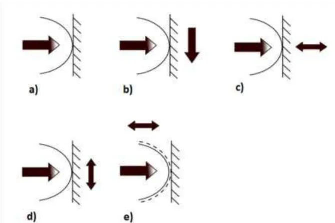
[image:3.595.138.474.471.695.2]Over the last 25 years commercial nanoindentation test instruments (also called nanoindenters) have improved their resolution, their calibrations and their ability to very precisely position where the indentations are made to obtain highly localised and accurate mechanical property information. Additionally, they have expanded the range of test techniques beyond simple nanoindentation, with several including some capability for nanotribological measurements (e.g. nano-scratch and nano-wear testing) which has consequently greatly expanded their range of applications. There are a range of commercial nanoindenter designs, including electrostatic or capacitive actuation, and vertical or horizontal loading configurations. The design of one popular commercial test instrument, the NanoTest from Micro Materials, combines electrostatic actuation with horizontal loading and an open test platform that has enabled its further development into a true multifunctional nanomechanical/nanotribological test instrument where tests can be performed with a range of contact geometries (figure 1) and environmental conditions (figure 2 illustrates the temperature and strain rate test envelope) [4]. The various tests provide complementary information and the data obtained can often more usefully map onto the actual conditions that the materials experience in use. It is becoming possible to move beyond basic characterisation to the development of increasingly accurate prediction of the surface behaviour.
Figure 2: Temperature and strain rate test capability in a commercial instrument (NanoTest)
2. Nanoindentation
2.1 Contact mechanics theory
Figure 3: Nanoindentation curves on fused silica, single crystal tungsten and sapphire (0001)
Illustrative nanoindentation curves on fused silica, single crystal tungsten and sapphire (0001) with a sharp pyramidal Berkovich diamond indenter are shown in figure 3. For a given indenter geometry the load-displacement curve recorded in a nanoindentation test can be thought of a “fingerprint” for a material as it contains information about the elastic and plastic properties of the sample under test. The slope of the unloading curve at any point is called the contact stiffness. In this analysis, the reduced modulus, Er, is calculated from the stiffness at the onset of the unloading S and the projected area of contact between the probe and the material Ac as
c r
A S E
2
where is the correction factor for the shape of the indenter. There is some on-going debate over the exact value though is commonly taken as 1.034 for the Berkovich indenter geometry. The reduced indentation modulus, Er, is directly determined in a nanoindentation test (also referred to as E’). However, the plane strain modulus, E* = E/(1-2), can also be quoted (e.g. in ISO14577 [1]) and when reporting nanoindentation data it is therefore necessary to specify clearly which modulus is being reported (Er, E* or E). Conversion of the directly measured reduced modulus to the Elastic (Young’s) modulus of the sample requires that its Poisson’s ratio be known or can be reliably estimated. As elastic displacements occur both in the specimen and in the indenter (the indenter is not completely rigid), the elastic modulus of the sample is calculated from Er using
i i
r E E
E
2 2 1
1
1
(2)
where E and Ei, and i are the elastic modulus and the Poisson ratio of the tested material and indenter, respectively. For diamond indenters, Ei and i are 1141 GPa and 0.07, respectively. When a diamond indenter is used (i) on fused silica with = 0.17, a reduced modulus of 69.6 GPa gives E = 72 GPa (ii) for ceramics and hard coatings is typically 0.2-0.25. For sapphire with = 0.235, an Er of 314 GPa is equivalent to E = 410 GPa. (iii) For tungsten with Poisson ratio = 0.28, Er = 320 GPa converts to E = 409 GPa. The mean pressure or hardness (H) can be calculated as
c A P
H
(3)
where P is the applied load. Nanoindentation hardness is defined as the load divided by the projected contact area. However, in the definition of Vickers hardness the actual rather than projected area is used resulting in a geometric scaling factor of 0.927 [5] and after correction for units a final relation of
HV = 0.094545 HIT (4)
where HV = Vickers hardness and HIT is the depth-sensing indentation hardness.
2.2 Practical considerations
2.2.1 Reference materials for calibration
Fused silica has proved the most popular material for calibrating nanoindentation instruments and the test probes (indenters) they use. It is inexpensive, highly polished, mechanically homogeneous and has relatively little time-dependent behaviour due to its high melting point (~1650 C). Typically its mechanical properties are quoted as H ~9.2 GPa, E = (72 +/- 1) GPa and Poisson ratio = 0.17. In practice actual values may vary slightly from different suppliers. For example, a recent certified reference sample obtained from the UK National Physical Laboratory was supplied with E = 73 GPa and Poisson ratio = 0.16.
Despite being a default a reference sample popularly used for both area function and frame compliance calibration, its mechanical behaviour in indentation is actually complex. Kermouche and co-workers noted that whilst normal glasses exhibit little densification on indentation anomalous glasses exhibit large densification and different fracture behaviour, and fused silica, which is the most anomalous silicate glass of industrial interest, can achieve 20% densification after indentation [6]. Its behaviour is more complex than is generally supposed since (i) its near surface properties may be reduced by hydration (ii) it is an anomalous glass whose elastic modulus increases with temperature [7] (iii) contact area determination can be influenced by radial dilation due to its high H/E [8] (iv) densification occurs under the indenter (v) cracking occurs at high load, dependent on the acuity of the indenter [9] (v) by having a very high H/E ratio its sensitivity to small errors in frame stiffness was rather low.
Table 1 multiple reference sample calibration (after [10])
Reference sample E Experimental (GPa) E Expected (GPa)
Fused Silica 71.8 ± 0.4 72
Tungsten 417.5 ± 4.6 410
Steel 220.5 ± 1.5 220
2.2.2 Choice of loading ramp
The standard contact mechanics treatment of the unloading curve data used to determine H and E is essentially based on elastic contact mechanics with no provision for time-dependency. It is important that time-dependent behaviour does not influence the accuracy of the elastic modulus so the experimental conditions (load history) should be modified accordingly. Chudoba and Richter have detailed the problems that can occur when the holding period at peak load is too short [11]. For soft metals, the combination of slow loading, a long hold at peak load and a fast unload ensures that the contribution of non-elastic behaviour during unloading is minimized, or negligible in most cases. An alternative approach currently beginning to find favour is to develop more complex analytical treatments that can handle the time-dependency.
2.2.3 Instrumental (thermal) drift
Since nanoindenters measure very small displacements high accuracy is required, i.e. data should not be influenced by any thermal or mechanical drift during the test duration. For less thermally stable instrument designs, a practical solution has been to indent as fast as possible, although as mentioned above this fast loading and low hold time at peak load may result in some anelastic deformation during unloading for highly creeping materials. For all instrument designs it is important that when holding for a thermal drift correction (typically on the surface under the contact load immediately prior to the loading ramp and/or at 90% unloading) that deformation due to creep or creep recovery is not erroneously thought to be due to thermal drift. An excellent example of this is the continuing extensive creep recovery that occurs on all polymeric materials. For highly stable nanoindenters this can be x100 greater than the real thermal drift so mistakenly correcting data for it introduces error. Similarly if the sample is very soft (e.g. solder) then the initial load for thermal drift should not be used as deformation during this period is likely to be dominated by creep rather than drift.
2.2.4 The international standard for depth-sensing indentation - ISO 14577 parts 1-4
The International Organisation for Standardisation (ISO) has released an international standard ISO 14577 parts 1-3 entitled “Metallic materials – Instrumented indentation test for hardness and materials parameters” in 2002, with Part 1 Test method, Part 2 Verification and calibration of machines, Part 3 Calibration of reference blocks. The recent extension to the ISO indentation standard (ISO14577 Part 4 - Test Method for metallic and non-metallic coatings) is also concerned with experimental best practice for the determination of accurate hardness and elastic modulus of coatings independently of the influence of substrate. This is discussed further below.
Figure 4: (a) Illustrative nanoindentation loading history for a metallic sample (b) indentation creep during 30s hold at peak load at 500 mN on single crystal Al (c) nanoindentation behaviour at 100-500
mN on single crystal Al
The suitability of the elastic unloading analysis for polymeric materials that show pronounced viscoelastic behaviour has been questioned for the same reasons. Nevertheless, a similar approach to that recommended above for metals has recently been applied to a range of commercial polymers by Young and co-workers at NPL [12]. The elastic modulus measurements showed reasonably good agreement with supplier quoted values (presumably from bulk methods) and a new atomic force microscopy technique using Hertzian contact mechanics. Dub and co-workers found non-constant elastic modulus vs. load for copper samples when following the ISO14577 approach [13]. The complex non-linear behaviour found was considered to arise from limitations to this method. Whilst the ISO standard does have some deficiencies and simplifications, in this case it is not clear that at least some of the experimental trend observed might have been due to the load history employed (constant loading and unloading time, in conjunction with no obvious hold at peak load for creep).
2.2.5 Surface roughness
2.2.6 Determination of frame compliance
Removal of the contribution of elastic bending of the nanoindentation instrument from the raw data is required before analysis to determine H and E. Frame compliance is the inverse of stiffness. It is common to use compliance rather than stiffness as the relationship is simply
Ct = Cs + Cf (5)
[image:9.595.51.544.250.543.2]Accurate determination of this frame compliance of the instrument is therefore essential, particularly for reliable modulus measurement. This can be done by direct or indirect methods. ISO 14577 describes both. The direct approach is less well-established but assumes nothing about the elastic properties of a reference material or the reliability of the contact mechanics and may prove increasingly popular in future. In principle a rigid contact is made between the load application part of the instrument and the rest of the frame so that all the measured deformation results from the compliance of the frame with a zero contribution from sample compliance [15]. The indirect method is much more common and relies on the sensitivity of the reference material(s) to the instrument stiffness and to the accuracy of the indenter area function used.
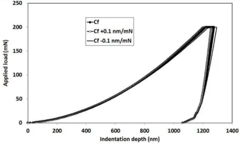
Figure 5: Indentation curve on single crystal tungsten after correction of frame compliance together with simulated curves with the frame compliance incorrectly determined
As an illustration of this, figure 5 (a) shows the indentation curve on a tungsten reference sample analysed with the correct frame compliance of 0.38 nm/mN for the instrument used. Figure 5(b) shows the true indentation behaviour together with simulated curves corrected for frame compliance of (0.36 + 0.1) and (0.36 – 0.1) nm/mN rather than the correct value. The high sensitivity of the tungsten reference sample to the value of the frame compliance used in the calculation is due to its low H/E ratio. Since accurate frame compliance also requires an actual area function, the use of multiple reference samples is attractive. ISO 14577 recommends the use of two reference samples with widely differing elastic modulus. Accurate frame compliance calibration is even more important as the load increases into the micro-range since the proportion of sample compliance to frame compliance decreases.
2.2.7 Determination of the area function
practice all indenters are slightly rounded at the very apex and area functions are usually improved by the use of more measurements at lower load in the fit so that the relationship is accurate in this range. Area functions can be simple or apparently complicated relationships. On the simpler side, a function of the type Ac = Ah + Bh2 is a reasonably robust approach which can often deliver modulus measurements to within about 2% of literature values across a wide depth range. It has the advantage of being able to be used to estimate the shape for depths above which calibration data exist so that measurements can be made on very soft materials. Nevertheless, not all pyramidal indenters are well fitted by such a simple relationship and polynomial fits (e.g. from 2nd order to 5th or more) or spline fits can be preferable in many cases. However, higher order polynomials should not be used outside of their fit range as they will diverge strongly. Another limitation of using fused silica is that above a threshold load (ISO14577 suggests 75 mN for a Berkovich indenter but the exact value will depend on indenter sharpness) it cracks. Although such cracking is relatively minor for the Berkovich geometry compared to indenter geometries with more acute angles where discontinuities can clearly be seen in the loading curves, the cracks are clear in SEM images of indentations and there will presumably be some subtle effect on the load-displacement curve even if obvious pop-in type features are absent.
ISO also notes the possibility of more directly measuring the area function with a traceable (metrological) AFM. This has the potential advantage that any issues concerning the accuracy of the contact mechanics used in the analysis such as radial dilation on fused silica [8] are eliminated but the AFM measurement itself may be subject to some uncertainty, particularly at shallow depths. Dub and co-workers have suggested that AFM measurements are typically subject to up to 7% error [13]. Nevertheless, in future the AFM-based calibration may become more popular, particularly for certifying the geometry of master indenters for cross-calibration purposes. For day-to-day calibration the indirect method is expected to continue to remain popular as the most convenient way to assess any changes in geometry of an indenter, e.g. after continued indentations into a hard tool coating or steel. In practice the area functions of new indenters can change significantly but often approach a quite stable, but not very sharp, geometry after a period of sustained usage.
2.2.8 Zero point correction
Precise surface detection and assignment of the exact point at which the initial contact was made are important requirements for accurate hardness and elastic modulus measurements, particularly at shallow depths. There are different strategies for doing this, based on whether pre-contact data are acquired or not. In one commercial instrument the zero point is defined by default at the position where the contact stiffness exceeds 200 N/m (~ x2 instrument spring stiffness). Moseson and co-workers have criticised this as being insufficiently reliable since they found it can lead to a false zero several hundred nm away from the actual point [16] although it is in widespread usage. The other main approach does not require pre-contact data, with surface detected when a pre-set contact force is reached. In the NanoTest, for example, the spring stiffness is typically x10 lower than in other nanoindenters and the initial contact force can be varied over a wide range (e.g. 0.5-50 µN) if required (minimised for accurate measurements in low-vibration environments, or significantly higher to combat high roughness and/or vibration levels). Since there is always some elastic deformation occurring before this point it is then necessary to correct the displacement data for the missing depth either assuming Hertzian (since even sharp indenters always have some rounding at the tip) elastic loading, or more generally power-law or linear extrapolation, as suggested in the ISO standard. An example of a Hertzian correction is given by equation 6 [5].
F = C(h – h0)1.5 (6)
When indenting into a bulk material with well-known elastic properties it is therefore possible to back-calculate the radius of curvature at the tip, provided the data used are only to a small fraction of the radius, using equation 7. Chiang and co-workers have noted that for the Berkovich the transition between the spherical end cap and the pyramidal shape occurs at hc = indenter radius/4 [17].
2.3 Indentation size effects
The onset of non-elastic deformation and the associated critical load can be marked by a displacement excursion (a “pop-in”) or change in slope but this is not often the case, particularly for sharper indenters. Below this point the indentation behaviour is fully elastic. It is often called the elastic-plastic transition and it marks the onset of dislocation motion in metallic materials, but in semiconductors pop-ins may be caused or complicated by phase transformation events occurring once a critical pressure is reached (e.g. pop-ins on Si usually occur when the contact pressure rises to about 12 GPa [18]). Sapphire is another material that can show well defined pop-in behaviour [19]. Dub and co-workers observed clear pop-ins of >50 nm on Cu (111) and Cu(100) at around 0.5 mN when using a 407 nm tip radius (blunt) Berkovich [13]. They reported mean pressure values at the moment of homogeneous nucleation of dislocations (i.e. at the pop-in load) for Cu (111) and Cu (100) surfaces of 16.8 and 9.3 GPa respectively. Before yield metallic materials can support much higher contact pressure than their hardness post-yield.
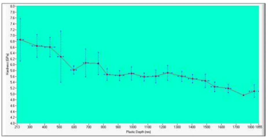
[image:11.595.66.530.269.508.2]Various indentation size effects (ISEs) can be observed, with hardness either increasing or decreasing as a function of depth. Several theories have been proposed to explain the most common ISE where hardness increases with decreasing indenter load, as in the example on tungsten shown in figure 6.
Figure 6: Polycrystalline tungsten shows a strong indentation size effect in hardness.
Arguably the most popular is gradient plasticity theory where geometrically necessary dislocations (GNDs) are generated under the indenter due to strain gradients. Decreasing the indentation size results in a greater density of GNDs and hence to higher measured hardness. The theory predicts that the total dislocation density within the plastically deformed volume varies as 1/hc, so that H2 1/hc. Nix and Gao fitted the hardness vs. depth dependence with a two parameter model, finding good agreement on a range of metals above indentation depths of 150 nm [20]. The two parameter model is shown in equation 8
H/H0 = [1 + (h*/h)] (8)
2.4 Choice of indenter geometry and stress-strain curves
Sharp indenters induce full plasticity at low load so that the mean pressure measured in the test is the hardness of the material. In general for a conical indenter the strain is proportional to the tangent of the cone angle and so is constant at different indentation depths (for a pyramidal indenter there is an equivalent angle). Blunt indenters, or spherical geometries, do not always generate full plasticity immediately and more force may be required. The strain induced by a spherical indenter is proportional to a/R and is a function of depth. This suggests the possibility to generate stress-strain curves by indentation, with the load partial unload technique being able to generate the entire strain curve in a single test. The stress-strain curve in a tensile test can provide the following information for structural design: (i) Young’s modulus (ii) yield stress (iii) work hardening exponent (iv) ultimate tensile stress (v) strain at failure. Tensile tests suffer from limitations in specimen size and reproducibility and the possibility to obtain equivalent information from indentation is being actively investigated by several research groups. With FEA it is possible to generate the indentation curve from tensile stress-strain data but it is more challenging to uniquely solve the inverse problem and generate a tensile stress-strain curve from indentation data. Three main methods are (i) representative stress and strain (ii) inverse analysis by FEA (iii) neural networks. Residual stress is an added complexity, with the indentation force required to reach a given depth under tensile stress being lower than in the stress-free state and under compressive stress the force required is greater.
2.5 Plasticity index and H/E
Plasticity in contact is governed by the roughness and elastoplastic properties of the contacting surfaces. In an indentation contact plasticity is directly correlated with the ratio of hardness (H) and elastic modulus (E) [23,24]. For a given indenter geometry the load-displacement curve recorded in a nanoindentation test can be thought of a “fingerprint” for a material as it contains information about the elastic and plastic properties of the sample under test. A useful dimensionless property is the plasticity index (PI) which is the plastic work done during indentation (Wp) divided by the total elastic (We) and plastic work done during the indentation, over a wide range of H/E values, with the relationship taking the apparent form
PI = Wp/(Wp + We) = 1 – x(H/Er) (9)
where x is a constant and Er is the reduced indentation modulus. Prior to the development of nanoindentation, a plasticity index was proposed that related the deformation in rough contacts to the ratio of Er/H multiplied by a geometric factor [25]. This original plasticity index is a general surface texture parameter that combines material and topographic properties of solids in contact. The equation originally developed by Greenwood and Williamson [25] is shown in Eqn. 10.
= (Er/H)(/) (10)
2.6 Hardness and elastic modulus of coatings
An often quoted rule of thumb is the so-called 1/10 rule where the relative indentation depth (RID = indentation depth/coating thickness) should be less than 0.1 to determine coating-only properties independently of the substrate [1,5]. In practice this usually works well for hardness but less well for elastic modulus. The ISO standard recommends Berkovich indenters should be sharper than 250 nm end radius for hardness measurement. Whilst this may not be really necessary for thicker coatings, sharper indenters are preferable for hardness measurements on very thin films. Accurate hardness measurement of a coating relies on development of a fully plastic zone within the coating. If the applied load is too small then the results can be influenced by surface roughness and the plastic zone may not be fully developed. If the applied load is too large then the plastic stress field may extend beyond the coating-substrate boundary and the measured response is therefore a composite of the plastic properties of both the coating and the substrate. Theoretical models based on approaches such as weighted area or volume law-of-mixtures have been developed to estimate the coating-only hardness from this composite response, with later work focussing on energy-based (work of indentation) models that have been adapted to include the effects of both plasticity and cracking [33].
As mentioned above, the elastic modulus measured at RID = 0.1 can be a poor estimate of the coating modulus, especially when there is a large elastic mismatch between coating and substrate. For example, Korsunsky and Constantinescu have predicted that when a coated system of Ec = 500 GPa, Es = 100 GPa,
c = 0.2, s = 0.3 (i.e. approximating to a stiff ceramic coating deposited on a much less stiff metallic substrate) is indented with a conical indenter the modulus is 25 % lower at a RID of 0.1 than the true coating value [33]. ISO14577 part 4 recommends making measurements over a range of indentation depths, provided that a/tc is less than 2.5, and extrapolating to zero depth to obtain a value of the coating modulus independent of substrate. In practice a linear extrapolation is a fairly robust approach which usually yields improved values from those determined from measurements to a RID of 0.1, although measurements to RID of 0.03-0.05 can also work well.
2.7 Ultra-hard coatings
Accurate and traceable calibration by methods such as ISO14577 can help validate or question the mechanical properties of new coatings. Veprek and co-workers have claimed deposition of ultra-hard nanocomposite coatings with hardness of ≥100 GPa (i.e. higher than diamond) [34]. This highly contentious claim has been the subject of an excellent critical review by Fischer-Cripps, Bull and Schwarzer [35]. These authors have provided compelling evidence for these reported hardness values to be over-estimated by a factor of 2. They were able to show that the analysis approach taken by Veprek and co-workers that obtained the correct hardness of a ultra-hard sample of known properties (industrial diamond) nevertheless under-estimated the elastic modulus by a factor of 3 proving that the calibration and analysis method was not accurate. Additionally, since the elastic modulus of the nanocomposite coatings in question was only in the region of 450 GPa, it should theoretically not be possible to produce coatings with hardness over 65 GPa due to the limit in H/E with a conical indenter.
2.8 Depth profiling
There are three popular methods for obtaining properties such as hardness, modulus and contact stiffness as a function of depth. These are (i) performing indentations to differing peak loads (ii) dynamic indentation (otherwise known as continuous stiffness measurement, or CSM) (iii) multi-cycle loading (or load-partial unload testing). The most obvious, although quite time-consuming, is simply to perform indentations at different locations with different peak loads and consequently stress fields. The CSM method has recently been called into question by Cordill and co-workers who noted that the oscillation used with dynamic indentation techniques alters the measured hardness value of ductile metallic materials, especially at depths less than 200 nm [36]. The alteration in the hardness is due to the added energy associated with the oscillation which assists dislocation nucleation. In other words, there is inherent risk in trying to determine properties by oscillation as you are completely changing the dislocation density of the material you are trying to measure.
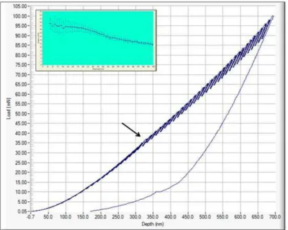
oscillation. Figure 7 shows an illustrative load-partial unload test result for a hard diamond like carbon (DLC) film deposited on silicon. The inflexion in the curve marks the point at which the plastic stress field is no longer completely within the coating and the measured hardness becomes a composite response of the coating and the softer substrate.
Figure 7: A 50-cycle load-partial unload test on a 2 m DLC film on Si. The inset shows variation in hardness with depth from repeat tests
2.9 Mapping and positioning
[image:14.595.90.509.94.429.2]Nanoindentation instruments have precision stages enabling accurate positioning in discrete phases to obtain highly localised mechanical property information. Experiments are typically performed as large automated arrays (e.g. 10 x 10 or 20 x20 grids of indentations) or more focussed tests involving a smaller number of indentations precisely positioned in the phases of interest.
An example of grid mapping is shown in figure 8. Here 400 indentations have been made into a Ti6Al4V aerospace alloy as a 20 x 20 grid. Average values of hardness and reduced elastic modulus were (4.5 ± 0.5) GPa and (139.7 ± 7.5) GPa respectively. More information is revealed in the hardness and modulus maps, with distinct areas of lower mechanical properties. Indentations can be placed closer together (e.g. 1-2 m pitch) to obtain higher resolution maps. In the example below inclusions of an Al7Cu2Fe intermetallic phase can be seen to have completely different mechanical properties to the bulk matrix.
Figure 9: Mapping the mechanical properties of an intermetallic inclusion in a 7000 series Al alloy
2.10 Fracture toughness
Depending on load, material, indenter geometry and environment, five major types of cracks occur in the indentation of brittle bulk materials or thick coatings [37]. These are: (a) cone cracks (b) palmqvist radial cracks (c) median cracks (d) lateral cracks (e) half-penny radial cracks. Fracture toughness can be determined from the crack systems by either stress-analysis-based or energy-based models. The application of these to the determination of the fracture toughness of thin coatings has been well summarized in an excellent recent review by Chen [38]. Lawn and co-workers showed that for a well-developed radial/median crack system i.e. half-penny like cracking caused by indentation that the Kc fracture toughness of the material was proportional to the applied load multiplied by the average crack length c raised to the power of -3/2 [39] (equation 11).
Kc = C(E/H)1/2P/c3/2 (11)
where C is a geometry constant commonly taken as 0.016 for Berkovich or Vickers and 0.032 for cube corner indenter geometries. However, as the thickness of the coating is reduced it becomes more difficult to apply this equation due to the interference of the substrate and interface with the coating crack system. If the load is reduced to avoid this complication then the crack system is not sufficiently well developed to apply the analysis. For thinner coatings the energy-based models refined by Bull and Chen can be more applicable [40].
2.11 Micro-pillar compression, micro-cantilever bending and push-out tests
deformation mechanisms at work. In macro-scale experiments such problems are obviated by using tensile or compressive load application to a sample of a known cross-sectional area. This produces a constant stress at any given point along the specimen (at least until plasticity is initiated locally). Modern sample preparation techniques, in particular Focussed Ion Beam (FIB) milling, now allow the manufacture of microscopic equivalents of the samples used in the conventional macro-scale techniques. The most popular sample geometry used is the micro-pillar [41-43]. There is also growing interest in Micro-cantilevers (or “bend bars”) which may be produced using the same technique.
Micro-pillar Compression
For almost a decade now interest has been growing in the field of micropillar compression experiments. Uchic et al used the technique to demonstrate size effects on the measured strength of Ni and three Ni based alloys [41]. They demonstrated that micro-pillars of practically manageable dimensions (0.5 to 40 µm diameter) were sufficiently small to show the relationship between strength and volume based phenomena such as dislocation nucleation and movement. Once the pillars have been produced they are carefully positioned in front of a flat topped indenter commonly known as a flat punch. This is achieved by positioning the sample precisely in the crosshair of the nanoindenter’s microscope then moving to the indenter position (the vector from microscope cross hair to indenter centre is calibratable and automatically executable on most nanoindenters to better than 1 µm precision). Once in position the load is applied to the micropillar using the flat punch indenter. The example below shows a load vs. displacement trace from a micropillar compression experiment. As can be seen, the data are easily converted to engineering stress and engineering strain due to the dimensions of the micropillar being well characterised and there being no constraining material surrounding that being tested.
Although pillars are the most common geometry for microcompression experiments, other structures have been tested. By compressing of variously shaped wall-like structures with differing length-to-width ratio Jennett and co-workers provided evidence that yield strength is determined by the smallest dimension of the structure (“thinness”) [44]. Their results showed that yield stress was determined by wall width with length playing little or no effect.
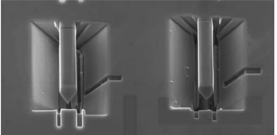
Micro-cantilevers
[image:16.595.67.531.525.752.2]Micro-cantilevers are produced in a similar manner as micro pillars. A FIB is used to cut out an elongated three sided trough leaving and island of material of the length and width of the required cantilever. The FIB is then re-orientated such that it can be used to undercut the cantilevers, allowing them room to deform as the load is applied.
Figure 11: SEM image of two micro-cantilevers cut into a silicon wafer. These samples have been prepared for brittle to ductile transition experiments over a range of temperatures and as such have had a crack initiation notch machined into them near their roots. These cantilevers are 4 µm wide and 15 µm
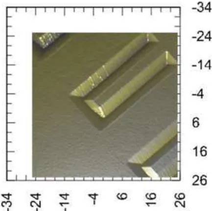
Similarly to micropillars, micro-cantilevers may be targeted using an integrated optical microscope but more commonly a 3D imaging stage is used. This allows the cantilever to be imaged whilst mounted on the nanoindenter. The sample is mounted on a high precision feedback controlled piezoelectric stage. The sample is either raster or bi-directionally scanned whilst the indenter is held on the sample surface under a very low load (~1 µN). The scan parameters are defined by the user, these include the dimensions of the imaged area and the resolution of the image (number of scanned lines). A 3D image of the sample is produced from a combination two sets of coordinates from the piezoelectric stage and the third set of coordinates from the indenter depth sensor.
Figure 12: 3D “nanopositioner” image of cantilevers machined into W. Note that the true cross-section of the cantilevers is not see due to the geometry of the Berkovich indenter used for imaging. Image size is
50 µm x 50 µm
The resultant image may then be used to select the point(s) at which the indenter is applied to the cantilever to apply the bending load. The distance between the root of the cantilever and the chosen contact point(s) are easily determined from the 3D image and as such the stiffness of the cantilever may be determined once the bend test has been completed. The stiffness value may then be used to determine the elastic modulus of the sample material using beam theory. This approach is well documented by Armstrong et al. [45] where cantilevers were FIB machined into selected copper crystals whose orientations had been previously characterised by Electron Back Scatter Diffraction (EBSD). The combination of the data from both techniques demonstrated the anisotropic nature of mechanical properties as a function of crystal orientation.
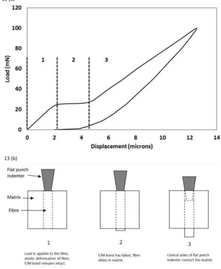
Fibre push-out
[image:17.595.188.405.171.387.2]Figure 13: (a) and (b)
3. Nanotribology (nano-scratch and wear)
Increasing use of thin films and coatings from a few nm to about 1 micron thickness for improved wear resistance in MEMS and general thin film applications requires their mechanical properties and tribological performance are optimised. Since the test conditions in the conventional macro-scale scratch test (R = 200
m) were specifically chosen for fairly thick (≥3 m) coatings they are not appropriate for much thinner films and nano-scratch and nano-wear tests are needed. These tests typically use considerably lower load combined with a smaller probe radius than macroscale tests to achieve the required combination of surface (and lateral) sensitivity and high contact pressure to drive film failure.
Integrated precision control of the movement of the sample stage independently of the load application during the test enables various topographic, scratch and wear tests to be performed. In the NanoTest, for example, there are four distinct types of test:-
[image:18.595.83.514.41.565.2](ii) Progressive (ramped) load scratch – either initially or after a set levelling distance a linear load ramp
(iii) Topography-scratch-topography (3-scan) test
(iv) Multi-pass wear tests - involving various combinations of topography and either ramped or constant load scans
The tangential (frictional) force can be recorded simultaneously, which provides valuable confirmatory information on the location of failure relative to the moving test probe.
3.1 Critical load sensitivity to intrinsic and extrinsic factors
Steinmann and co-workers showed that the critical load in the scratch test can be influenced by a range of extrinsic and intrinsic factors [47]. The influence of the scan parameters of loading rate and scan speed on the critical load has been investigated for a range of Si-doped DLC coatings on glass that show clear film failure in nanoscratch tests [48]. There was considerably less sensitivity to these scan parameters than has observed in macro-scale scratch testing. At the macro-scale the dL/dx ratio, where L = normal load and x = scratch distance, was found to be an important parameter, with the critical load decreasing when dL/dx decreases. Steinmann and co-workers recommended tests be done with a fixed dL/dx of 10 N/mm, suggesting that when dL/dx decreases, the probability of encountering defective adhesion within a certain load range increases resulting in a decreased critical load. This explanation may not be true for highly homogeneous coatings that do not fail by selective failure of poorly adhering regions and so exhibit very consistent Lc values, and also does not consider the possibility of cohesive failure.
In contrast at the nano-scale, no dependence on critical load was found for Si-doped DLC coatings on glass on either (1) scratch speed, (2) loading rate, or (3) increase in load per unit scratch distance (dL/dx) when dL/dx is much less than 1 N/mm, whilst critical loads only slightly increase at higher dL/dx (1-5 N/mm). More recently Beake and co-workers have investigated the variation in critical load for failure of a 80 nm ta-C film on Si over a 100 fold range of dL/dx without finding any clear dependence [48]. These results suggest that nano-scratch tests under significantly different loading conditions can be compared directly.
3.2 Topography-progressive load scratch-topography multi-pass scratch tests
Figure 14: Load vs. depth curves in nanoindentation and nano-scratch tests on Si(100) with a 4.6 m spherical probe
By performing three-scan progressive load nano-scratch tests it is possible to determine the critical load for the onset of non-elastic deformation since this is the load at which the residual scratch depth is no longer zero. The mean pressure at this point can be used as an estimate of the yield pressure. By increasing the load further it is possible to identify the critical loads for transitions for cracking and delamination events and converting these to mean pressures.
3.3 Influence of probe radius and geometry
The choice of probe radius in the nano-scratch test should be considered carefully. Spherical probes with end radii typically 1-10 m are commonly used for nano-scratch testing. If probes are too blunt or the instrument used has a relatively small maximum load then it is not possible to scratch the coatings to failure. Sphero-conical probes with ~5 m end radius represent an effective choice ensuring that coating failure is observed within the force range of the instrument but without risking rapid blunting of the indenter due to repeat scanning that can be observed when sharper probes are used (such as Berkovich indenters), especially when scratching hard and rough coatings. The use of the spherical indenters has the additional advantage that the contact pressure analysis described below can be directly applied to the nano-scratch data, provided the instrument software has the capability to remove the contribution of instrument compliance, sample slope and roughness from the measured deformation data so that true nano-scratch and nano-wear depth data is displayed. Pre-calibration of the indenter radius by nanoindentation is necessary.
Figure 15: Influence of interlayer composition and thickness on critical load for Pt-Ir coatings
This appears to be a good example of dimensioning, where the probe sharpness was increased to improve the sensitivity to the adhesion at the interface. Schwarzer and co-workers have used advanced simulation tools to “dimension” macro-scale scratch tests of thick multi-layered cutting tool coatings [14]. By adjusting the scratch probe radius and applied load they were able to show the possibility to adjust the position of the depth of the maximum von Mises stress in multilayer coatings. By appropriate “tuning” they could position the maximum stress near the different interfaces in the coating-substrate system.
There have been occasional reports that the scratch depth under load may be greater for constant load than in progressive load testing but this does not appear to be the case in general. Beake and co-workers reported that for TiN on tool steel the deformation in constant load and ramped load tests was almost identical at the same load [53]. This implies that the critical load obtained in a progressive load scratch test is a reliable choice of determining a fractional sub-critical load to assess the film resistance to low cycling fatigue in a nano-wear test.
3.4 Contact pressure
Recently the capability of the progressive load multi-pass scratch technique has been extended by the development of a novel analytical treatment to obtain accurate scratch depth data after correction of the raw data for the contribution from instrument compliance, sample topography and sample slope [54]. The method described in reference 54 enables the yield stresses and the pressure required for the failure of the film to be estimated from contact mechanics, assuming the geometry of indentation, provided spherical indenters are used. By using spherical probes the contact depth (hp) in an indentation contact is given by
hp = (ht + hr)/2 [Eqn. 12]
where hp is the contact depth, ht is the on-load scratch depth and hr is the residual depth from the final scan. The contact radius (a) is determined from Equation 13, where R is the indenter radius.
a = (2Rhp-hp2) [Eqn. 13]
Pm = L/a2 [Eqn. 14]
The contact pressure, Pm, at any point along the scratch track is given by equation 14, where L is the Applied load. To apply this approach to the nano-scratch data it is necessary to assume that:
(1) the presence of a tangential load does not influence the pressure distribution too greatly (i.e. that the measured friction coefficient is well below 0.3)
(2) the radius of the indenter is constant
(3) the sliding speed is sufficiently slow and contact sufficiently close to elastic that the load is supported on the rear of the indenter
In practice it appears that these conditions can often be met in the nano-scratch test [54, 55], although the approximation becomes less valid as the geometry moves away from Hertzian. The methodology has been validated for thin films on Silicon wafers with good agreement between (i) scratch hardness independently determined from optical measurements of scratch widths (ii) contact pressures for film and substrate yield events.
3.5 Influence of film stress and thickness
Beake and co-workers have reported nanomechanical and nanotribological (nano-scratch and nano-wear) characterisation of a wide range of thin films on Si, with thicknesses from 5 nm (ta-C) to 1500 nm (TiN) performing nanoindentation with Berkovich indenters combined with nano-scratch testing with spherical indenters [49, 54-57]. A key motivation for studying several of these was to understand the interplay between film thickness and interfacial toughness for MEMS and protective thin film applications. The reliability of Si-based MEMS devices is limited by stiction forces when contact occurs. Applying very thin, low surface energy and low stress coatings can alleviate this problem but it is critical that they are deposited optimally.
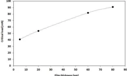
[image:22.595.78.516.394.656.2]The film thickness is a key parameter influencing the critical load in the nano-scratch test. In principle, film thickness can have two opposing effects:- 1) thicker films that are harder than the underlying substrate provide more load support and so delay the onset of the substrate deformation that is often the precursor of film failure (higher critical load) 2) thicker films can be more highly stressed and more easily through-thickness crack and delaminate when deformed (lower critical load) since the driving force for spallation to reduce stored elastic energy is greater. The relationship between film thickness and critical load can be quite complex in practice.
Figure 16: Variation in the critical load of 5-80 nm ta-C films on Si with thickness
Shi and co-workers reported nano-scratch data for 200 nm and 1000 nm a-C films deposited with varying substrate bias voltage (-20 to -140V) by closed field unbalanced magnetron sputtering (CFUBMS) [57]. They found that on wear resistance grounds a suitable strategy for optimising wear resistance for MEMS applications was to maximise H/E. For 200 nm films the highest H/E materials performed best since the intrinsic stress in the film was relatively low (no recovery spallation and low H/E). For ~1 µm a-C films they observed a general relationship between H/E and the scratch test critical loads. When H/Er is ~0.09-0.1 there was a tendency of the films to delaminate behind the moving probe at low critical load. Beake and co-workers previously reported a similar correlation for ~0.8 m Ti-Si-N nanocomposites films on Si [50]. Higher H/E led to higher critical loads for elastic-plastic transition and also for the total film failure occurring in front of the probe. However, when H/Er was >0.09 film failure was always by tensile failure behind the probe (also described as unloading failure). The high tensile stress behind the probe in the nanoscale scratch test can lead to complete failure for hard films on silicon. More information can be provided by nano-wear tests.
3.6 Repetitive nano-wear
Constant load, unidirectional multi-pass scratch testing was first described by Bull and Rickerby in 1989 [58] and has been shown to be an effective low cycle fatigue test. The same approach can be applied to micro- and nano-scratch testing. Constant load nanowear tests are often used to determine rates of sliding/abrasive wear and investigate the role of fatigue. The low-cycle nanowear experiments can often be much more informative regarding the influence of thin film stress leading to poor adhesion than single scratch tests. When compared to progressive load nano-scratch testing, nano-wear testing has the advantage that the load can be varied to tune the maximum von Mises stress to be close to the coating-substrate interface. The friction force is sensitive to the onset of coating failure.
Shi and co-workers performed sub-critical load nanowear testing to investigate the performance of 1 m a-C films that fail in single nano-scratches at ~200 mN [57]. The wear test loads were chosen so that the maximum stresses were either within the film (at 50 mN) or the substrate (at 150 mN) so that the additional stress due to the imposed stress field from the scratch reaches the interface for the higher load test. In the lower load wear test the contact is almost completely elastic with residual wear depths under 100 nm. An approximately inverse correlation between H/E and the residual depth was found, consistent with the work of Matthews and Leyland who have shown that increasing H/E reduces plasticity [28-29]. An increase in residual wear depth and decrease in scratch recovery with each wear cycle confirm that the low load multi-pass wear test is a fatigue process. In marked contrast, the films failed after a few cycles at 150 mN. As 150/Lu = 0.7 this is perhaps not too surprising, particularly as the load is great than that at which initial edge cracks form (Lc1). Nanowear under these conditions is a very low cycle fatigue test where plasticity and micro-fracture dominate and the harder films deposited under high bias perform poorly. The behaviour of 1 m a-C films with a very high ratio of H/E, deposited under high substrate bias, is very strongly dependent on the test conditions, performing well at low load wear but very poorly in more highly loaded contact. They exhibit low critical loads in progressive load scratch tests and when they fail in the nano-wear test there is extensive delamination outside of the scratch track. The combination of nano-wear tests at different loading levels provides information regarding the suitability of the a-C films for contact applications.
Figure 17: Influence of increased thickness and load support on critical load in the micro-scratch test
3.7 Surface roughness
Beake and co-workers have recently investigated the influence of coating thickness, roughness and the direction of scratching relative to grinding marks on the behaviour of TiN coatings on M42 steel in single and multi-pass nano-scratch (nano-wear) tests [53]. TiN coatings were deposited on M42 steel as this is a model system displaying clear failure with comparative frictional data available from previous macro-scale scratch testing. The critical load for delamination failure was dependent on coating thickness and scratch orientation relative to polishing marks on the surface made prior to coating deposition. High roughness tends to decrease the critical load but the load carrying capability of higher thickness can have a much greater effect. Despite being much smoother, the critical load on 500 nm TiN was only ~50% of the critical load on the 1500 nm TiN. The critical load was 20 % lower when scratching perpendicular to the grinding marks than parallel to them.
3.8 Friction
The friction force in the nano-scratch test can be deconvoluted into its interfacial and ploughing components so that the interfacial friction can be reported:-
total = interfacial + ploughing
This can be done by different approaches: (1) performing constant load friction test at very low force where contact is completely elastic and the ploughing contribution is zero (2) performing repetitive scratches to eliminate the ploughing contribution (3) performing progressive load scratch and extrapolating the low load friction data to zero load.
Figure 18: Variation in friction with number of wear cycles
4. Nano-fretting
Miniaturisation of mechanical devices results in severe contact conditions generated by relatively small forces. Performance of materials at small contact scales is a significant challenge and tribology becomes an enabling technology for any small scale devices with moving components. According to the Amontons' law, the friction force is independent of the apparent area of contact, however the law does not hold true when the contact area is dramatically reduced. Fretting experiments performed at small contact scales bring specific challenges including increased importance of surface energy and adhesion, role of wear particles and impact of surface roughness.
Nanotribology research involving nano-fretting investigations tend to focus on two main areas related to (i) fundamental science leading to the understanding of basic principles of friction and asperities contact, and (ii) applied research related to technology of small devices like nano- and micro-electromechanical systems (N/M-EMS) where the standard constructs of classical physics do not always hold true. So far most of the work conducted on reduced contact scales has been focused on friction, however with novel measurement and modelling techniques established in recent years, nano-wear problem has been attracting more attention and interesting results are becoming available.
4.1 Fretting damage
Fretting is considered as a specific type of reciprocating sliding. It is defined as a small displacement amplitude oscillatory motion (usually induced by vibrations) between two nominally stationary solid bodies in contact under normal load. Depending on the loading conditions (displacement amplitudes, normal loading) fretting causes damage by surface fatigue or wear induced by debris formation. Fretting is indeed a complex process and not all the kinetics and mechanisms are well known. Collins defined more than 50 factors that influence fretting [60] and more factors are still being added [61].
Two major test configurations have been developed for fretting experiments (Fig. 19):
• fretting fatigue configuration, derived from a classical fatigue test where two pads are pressed on the fatigue specimen. Relative displacement () and cyclic tangential load (Q) are induced by the strain generated through the fatigue part subjected to external loading. In this configuration crack nucleates and then propagates due to applied external loading.
Figure 19: Fretting test configurations
The most established fretting test configuration used in fretting wear experiments is ball-on-flat one. In such configuration, the ball is subjected to normal load (P) or rotational load (Pr), Fig. 20, and three fretting modes can be distinguished [62]:
• linear displacement (mode I) • radial displacement (mode II)
• circumferential displacement (mode III)
Figure 20: Three basic fretting modes with representative displacement tracks
Most published research is focused on fretting mode I because the wear and friction mechanisms in that case are described by similar laws as sliding friction. However, other modes are also encountered in industrial applications and need to be investigated as well. The fretting mode II occurs in mechanical systems such as ball bearings or electrical contacts while fretting mode III can be observed in the specific areas of heat exchangers or steam generators.
Literature sources quote different values of displacement amplitudes as a border between the fretting process and reciprocating sliding motion. This value is variously interpreted and contained within a wide range of amplitudes, typically between 50 and 300 m for classical macro-scale experiments [63-66]. Although it is possible to limit the relative displacements between particular elements of mechanical systems by means of engineering measures, it is nearly impossible to eliminate fretting entirely, as this kind of degradation was reported even for displacement amplitudes less than 1 m [67-68]. The upper limit of fretting regime can be determined using the coefficient introduced by Fouvry S. et al. [69], which is defined as a sliding ratio:
where:
g – sliding amplitude, which is different from the displacement amplitude due to the contact and testing device compliance;
a – contact radius.
Figure 21: Definition of sliding ratio “e” and identification of transition between fretting regime and reciprocating sliding motion (contact sphere/plane), [after 69] .
The tribo-system remains in the fretting regime when the unexposed surface is maintained at the centre of the fretted surface (e < 1). The system moves into reciprocating sliding regime when the centre of contact area is becoming exposed to the atmosphere (e > 1).
Small scale fretting
Analytical tools for nanoscale materials have rapidly developed over the last three decades, improving resolution and efficiency of existing techniques and enabling development of new tools. Starting with the invention of the Scanning Tunnelling Microscope in 1981, various experimental methods based on Scanning Probe Microscopy (SPM) have revolutionised many areas of science and engineering by offering a wide range of resolution from the subatomic level up to few hundreds of micrometers. Among various SPM techniques, Atomic Force Microscopy (AFM) has contributed to the opening of a new chapter in the field of study of interaction of surfaces in relative motion at small scales, allowing for precise tests to be carried out under ultra-low loads and minute sliding distances. Nevertheless, it has been also shown [70] that AFM techniques are not fully suitable for testing MEMS applications as they offer much smaller sliding speeds compared to the real MEMS devices. This is where other novel micro-scale mechanical testing methods fill the measurement gap, which has been identified between conventional tribometers and AFM techniques (Fig. 22) [71].
[image:27.595.126.469.101.304.2]
Following the nanotechnology definition, nanotribology is typically defined as a branch of tribology that deals with wear dimensions of less than 100 nanometres. Currently, there is no formal nano-fretting definition available, however based on nanotribology description and sliding ratio criterion introduced by Fouvry et al. [10], nano-fretting can be defined as: “Small displacement amplitude oscillatory motion between two nominally stationary solid bodies in contact under normal load, with the unexposed surface maintained at the centre of the fretted surface resulting in wear depth of less than 100 nanometers.” This definition is limited to mode I fretting regime, however it can be easily adapted to modes II and III by modifying the aspect of unexposed surface area within the wear track. Although this definition captures the nature of nano-fretting regime clearly, most of the current literature claiming to report nano-fretting results would probably not fit into it. For the purpose of simplicity, these types of experiments are described as small scale fretting in this book chapter although they could also be described as nano/micro-wear for example.
Small scale fretting data have been reported by several research groups carrying out experiments on various, commercially available and purpose-built equipment. Varenberg et al. studied partial and gross slip fretting behaviour of 3.1 m diameter scanning probe microscopy probes tested against Si wafers [72]. A substantial increase of the coefficient of friction was noted at the transition between partial and gross slip fretting regimes by testing a range of sliding amplitudes from 5 to 500 nm. In collaboration with the same research group, Yoon et al. investigated impact of surface roughness and materials combination on fretting wear in a micro-spherical contact using 200 m diameter spherical tip under 20 mN load and 6.5 m displacement amplitude [73]. It was found that the materials combination has a greater effect on fretting wear behaviour than surface roughness in this small scale experiments.
Small scale fretting behaviour of monocrystalline silicon for potential application in MEMS devices operating in vacuum conditions was studied by Yu et al. using AFM tips [74-75]. The energy ratio related to the transition from partial to gross slip regime was measured and compared to the same energy ratio observed in classic macroscale fretting. The authors looked also at 2 nm thick DLC coatings deposited on Si(100) and carried out tests against SiO2 microspheres under vacuum and air conditions [76]. They found that DLC coating reduced significantly adhesion and friction force in air conditions comparing to Si(100) substrate, however wear behaviour was quite similar to that of Si. Wilson et al. focused on C and Cr doped amorphous C films and carried out small scale fretting experiments using a modified nanoindenter (NanoTest) with 300 m diameter ruby tip under 10-200 mN applied load and 2-14 m displacement amplitude [77-79]. The authors identified two distinct fretting wear regimes, with classic W-shaped wear scar under low oscillation amplitude and full U-shaped wear scar at larger amplitudes. Finally, micro-wear behaviour of DLC and TiN coatings using microtribometer setup under reciprocating sliding was investigated by Achanta et al., where the wear mechanism and topographical changes within the wear tracks were investigated using AFM analysis [80-81].
Indentation, scratch and small scale fretting on Si
There has been considerable interest in the mechanical characterisation of silicon for many years, however highly complex mechanical and tribological behaviour of silicon-based MEMS technology remains a main challenge. Nanoindentation of silicon has been the subject of number rigorous studies [82-85], but less is understood about its behaviour under more complex mechanical situations. Small scale tribology experiments require high resolution equipment with ultra-low drift, ideally 0.005 nm/s or less, to allow measurements of wear occurring at low contact pressures over periods of 1h or more. Typically AFM methods have been used for such experiments, however this piezo-based technology cannot provide necessary stability for long duration tests [86]. A number of micro-tribometers have been adapted for small scale tribology experiments but these are usually based on cantilevers to measure forces, which do not provide enough stiffness to carry out tests under very low displacement oscillations [87-88]. Hence, nanoindenter platforms have been recently modified for different types of reciprocating testing under milli-Newton range constant or ramped applied normal loads [88].
load, tangential loading in scratch and fretting experiments promoted yield resulting in higher penetration depths. SEM analysis of silicon samples revealed that pronounced lateral cracking observed under scratch and indentation conditions at high loads was absent in fretting tests, suggesting that the accumulation of strain is reduced by the more dynamic wear process. Critical loads observed in the three types of contact are summarised in Table 2.
Figure 23: Comparison of loading curves in indentation, scratch and fretting experiments. Test configuration: 4.6 m sphero-conical diamond indenter against Si(100). [Adapted from 55] .
Table 2. Critical loads small scale indentation, scratch and fretting experiments. [After 55] .
Critical load (mN)
Indentation Scratch Fretting
Ly 40 5 37 5 ~30
Lc1 ~80-95 56 4 *
Lc2 >200 106 7 *

![Carrefours Newsletter [Forward Studies Unit] April 1999 No 10](data:image/gif;base64,R0lGODlhAQABAIAAAP///wAAACH5BAEAAAAALAAAAAABAAEAAAICRAEAOw==)