International Journal of Innovative Technology and Exploring Engineering (IJITEE) ISSN: 2278-3075, Volume-8, Issue- 6S4, April 2019
Abstract—In this paper for proficiently dealing with three of the most generally utilized fundamental circuits, for example complementaryl metal-oxide semiconductor (CMOS) operational enhancer circuits A Metaheuristic search Algorithm called Modified Particle swarm Algorithm (MPSO) is appeared as a mechanical get-together. The MPSO estimation begins the framework by making some principal enthusiastic happy plans and using condition based for precariousness of these methodologies towards and outwards the best methodology. Promptly, the transistor estimations of the above-said circuits are refreshed utilizing MPSO to improve the structure focal motivations behind the circuit by rapidly lessening the district required by the transistors in a circuit utilizing MATLAB. By then the parameters are gotten are approved utilizing CADENCE. Here three operational intensifiers are anticipated model Two-plan operational intensifier, Folded course operational speaker and Telescopic operational enhancer. Ideally organizing clear circuits, the extension results and mix plots exhibit the consistency of adjusted molecule swarm improvement estimation over obtained figuring and molecule swarm algorithm. Keywords— Design Automation, Modified Particle Swarm Optimization Algorithm, CMOS circuit sizing; Two-Stage Operational Amplifier, Folded-Cascade Operational Amplifier and Telescopic Operational Amplifier.
1. INTRODUCTION
Digital design is more computerized compare to design of analog component so that, analog circuit experience high execution time and high cost. Generally, the efficient design of analog circuit categorized into (I) information based (ii) progress based. The learning based structure do data of originator to draw-up plan rule and the game plan takes quite a while, wearisome business and isn't reasonable for few circuit topologies. The another structure thinking takes on target fill in as restrictions, gives cautious outcomes. Models: Delight style [7], ASTRX/OBLX [8], IDAC[9], and so forth. The analog part design is more time taking and bulky task by hand, so it is required to computerize an analog circuit part, for final SOC design accuracy increases and cost reduces. The The quick PC cared for strategy (CAD) instruments unites the going with parts:[2]
1. Circuit topology assertion 2. Transistor looking over 3. Association structure.
This paper mainly focused on circuit sizing leads towards the sizing of chip area. The sizing tools of analog circuit
Revised Manuscript Received on April 12, 2019.
E.Srinivas, Research Scholar, JNTU Hyd, Hyderabad.Telangana, India. (E-mail: [email protected])
M. Sandhya,M.TechStudent,Dept.of.E.C.E, T.SAnurag Group Of Institutions, Hyderabad.Telangana, India.
M.VenkatSai,M.Tech Student, Dept.of.E.C.E, HyderabadAnurag Group Of Institutions, Hyderabad.Telangana, India.
integrated with synthesis & optimization parts. The improvement part is most gigantic one showed up especially in relationship with union part. Advancement systems are related with circuit structure computerization domains, for instance, section surveying, [3] enabled circuit yield enhancement,[4] and affirmed development (IP) center improvement. [5] In reasonable, the issue of the puzzling structure computerization can be loosened up by goodness and impacting properties as for an improvement tally, [6] accomplish the ideal blueprint. To make tracks in a contrary bearing from the zone optima which were a consequence of standard update estimation immaculate plan, the replicated toughening (SA) and developmental check (EA) [7] were showed up. To crash the neighboring optima, [8] the information parameters of reenacted toughening, the beginning stage and temperature respects are precisely chosen. Fitness function of the problem has been improved by applying iterative operation in evolutionary algorithm. Off spring optimal solution is generated by using crossover and mutation operator in genetic algorithm [9-10]. Off spring is generated by using mutation and recombination operators [11] in differential evolution algorithms. The resting part of this paper is as follows: Sec II describes an Analog Integrated Circuit Structure and its design specifications. Sec III presents the proposed Modified PSO Technique for Analog Circuit sizing method.Sec IV describes the simulation results and discussion. Finally, Sec V is the conclusion of work.
2. ANALOG INTEGRATED CIRCUIT
STRUCTURE:
Transistors, parasitic capacitance and resistor (non-linear) which are more sensitive of higher order effects, are the basic components in analog circuit [19]. Here, CMOS Operational amplifiers optimal design methods has been presented. To provide the operational amplifier circuit design parameter the hybrid MPSO is used [21], which should satisfy the design specification.The CMOS Amplifier circuit design specifications are: DC Gain, Slew Rate, Transistor Area, Power Consumption, etc. The design variables for CMOS circuit design are transistor length and width and input bias current. The proposed CMOS circuit major function is to optimize the design variables leads to reduction of the total chip size.
A Research Optimization of CMOS Analog
Circuits using Modified Particle Swarm
Algorithm
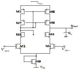
2.1. CMOS Two-Stage Operational amplifier design criteria Historically, two stage circuit architecture for both bipolar and CMOS operational amplifier has been the most popular approach. To drive resistive loads, more modern designs are used whose performance is very close to two stage operational amplifier. Fig 1 is having two gain stages with unity gain buffer stage if needed known as two-stage operational amplifier circuit. The first and second gain stages are differential input single ended output stage, common source gain stage with active load respectively. Capacitor Cc is used between the input and output of second
stage of an operational amplifier with feedback to establish stability. The effect of capacitance load(Cc) on the first stage
[image:2.595.330.527.211.341.2]is larger than the physical value called as Miller Capacitance. To provide more gain and swing we are used a two stage operational amplifier. N-channel differential input pair with an N- channel current mirror active load used as first stage of two-stage operational amplifier. The gain of the second stage is about 5-15 dB which is moderate. The second stage provides large output swing is critical for some applications which are with lower supply voltage. So, basic amplifier like a CS stage used as a second stage as shown in fig
Fig 1: Two- Stage Op-Amp
Parameters Specifications Open Loop
gain 86dB
Unity Gain
Frequency 5MHz
Slew rate >5V/µs
Phase Margin 60deg
Power
Consumption ≤50µW
MOS Transistor
Area 100µm
2
No of iterations 20
Table 1: Specifications of Two Stage Op-Amp
2.2. CMOS Folded Cascode Operational Amplifier design criteria
To choose the DC input voltage at Vin, convenience in shorting the input and output feedback configurations, higher voltage swing folded cascade amplifier has more ability. To achieve good input common mode range the output stage combined with uncommon architecture of differential amplifier are cascaded called as folded cascade
operational amplifier in fig 2.The transistor M1-M2, M4-M7, M8-M11 are differential output differential folded cascade amplifier at input stage has more trans conductance compared to pmos device and cascade current mirror which provides high gain of this stage respectively. The second post repeat is higher than the non winning shaft of a standard two stage topology. The compensation for this enhancer terminations to ground rather than the two stage pay style, and it has better irregular power supply rejection ratio(PSRR).
[image:2.595.62.277.344.472.2]Compared to telescopic topology this topology consumes more power, because of M10 &M11 acts as current source.
Fig 2: Folded-Cascode op-amp Using NMOS input devices
Parameters Specifications
Open Loop gain 70Db
Unity Gain Frequency 100MHz
Slew rate >100V/µs
Phase Margin 60deg
Power Consumption ≤100µW
MOS Transistor Area 100µm2
[image:2.595.62.275.352.630.2]No of iterations 20
Table 2: Specifications of FoldedCascode Op-Amp
[image:2.595.317.534.377.498.2] [image:2.595.85.255.495.673.2]International Journal of Innovative Technology and Exploring Engineering (IJITEE) ISSN: 2278-3075, Volume-8, Issue- 6S4, April 2019
Fig 3: Telescopic Amplifier Topology
Telescope operational amplifier has limited output swing smaller than folded cascode is the disadvantages since the tail transistor directly cuts into the output swing from both sides of the output. M1-M2 transistors are the tail current, M7-M8 transistor are gain and all the transistor are in saturation region.
Parameters Specifications Open Loop
gain 50dB
Unity Gain
Frequency 1000MHz
Slew rate >100V/µs
Phase Margin 60deg
Power
Consumption ≤100µW
MOS
Transistor Area 100µm
2
[image:3.595.101.240.53.174.2]No of iterations 20
Table 3: Specifications of Telescopic Op-Amp
3. PROPOSED MODIFIED PSO TECHNIQUE FOR
ANALOG CIRCUIT SIZING
3.1 Particle Swarm Optimization
In 1995[1], Doctor Kennedy develop a molecule swarm update structure which is meta heuristic technique. PSO is in like way a swarm understanding estimation like Genetic figuring (GA), Ant settlement streamlining (ACO, and so forth [2][3] in which the check earnest thought is on the swarm, direct of get-together of winged animals and school of fish and their improvement rather than essentially isolating for a particular animal. Winged creatures generally smell the sustenance from the far spot. Right when a feathered creature gets smell of sustenance, the bird starts moving towards that direction and the bird will communicate with the other birds regarding the food place and the direction. We can notice that, when a large group of birds moving in a particular direction tells the higher amount of food present in that direction. For the implementation of PSO, same method is used. Population of particles or swarms of solution are assumed a swarm of birds and the movement of particle or solution is assumed as movement of bird with some other function within the boundary. Equation 2 is the position updating equation. In PSO, every iteration will not give the appropriate solution, but gives some information regarding the solution. Using co-operation from
other solutions the most suitable solution is searched locally and globally to get the best solution of the problem like birds share the information locally and globally, the position is updated by using position updating equation. The birds moving in the space may or may not get the food particle; their food is the most optimist information than the other importance of every bird. Travelling sales man problem (TSP)[4], for training artificial neural networks (ANN) [5], etc can be solved by using this method. For computation environment the searching optimized solution is the particle swarm optimization (PSO) like multi agent parallel search algorithm. New position of particle is updated by using position and velocity equation 1 and 2 from the previous position by giving velocity to the particle. After random initialization of particles in the search space the particles starts allowed to with assigned velocities. To update the particle position this velocity is being used and we can find the personal best position (pbest), global best position (g best)
of entire swarm. For their first iteration Pbest will be the
current position and gbest will be the best of all gbest. After the
calculation of pbest and the gbest for all particles, the new
velocity can be calculated using equation 1 and position can be calculated with the updated velocities using equation 2
𝑉𝑖𝑛 +1= 𝑊. 𝑉𝑖𝑛+ 𝐶1. 𝑟𝑖1𝑛 . 𝑝𝑖𝑛− 𝑋𝑖𝑛 + 𝐶2. 𝑟𝑖2𝑛 . 𝑝𝑞𝑛− 𝑋𝑖𝑛
→(1)
𝑋𝑖𝑛+1= 𝑋𝑖𝑛 + 𝑉𝑖𝑛+1 →(2)
Here 𝑉𝑖𝑛 +1= Velocity of ith particle for (n+1) th iteration.
W= Inertia weight [6] used for controlling the velocity. Constant C1, C2 = Cognitive coefficient, Social
coefficient.
r1, r2= random numbers and it is between 0 and 1
If the particle may stay far behind than the targeted field, then the capacitor c1 and c2 values are too small, if the
capacitors are too big then they may fly away from the target field. The particle best (Pbest) global best (gbest) are Pin
and Pgn respectively.
[image:3.595.338.543.515.833.2]3.2 Weighted Particle swarm Optimization (WPSO)
To find the most importance solution and it doesn’t find the most importance best situation we use PSO algorithm. We will give the weight value for each particle in WPSO also. To introduce a weight parameter by calculate the mean best position and it importance to calculate the value of m by using the (gbest) global and (pbest) local searching
[image:4.595.327.528.50.324.2]capability. The evolutionary algorithms that companion best with the particles fitness value in WPSO. The mean best position is used to search scope of the particle, average on the best position. The most important particle is greater fitness value.
Fig.5. Weighted Particle Swarm Optimization Algorithm
A single particle gas has its own weighted value and each value of the weight is equal to 1 as shown in fig 5. Every particle has its own weighted value by using the mean best position.
𝑊𝑖 𝑛
𝑖=1 = 1 →(1)
WPSO=𝑊1∗𝑃𝑏𝑒𝑠𝑡+𝑊2∗𝑃𝑏𝑒𝑠𝑡+𝑊3∗𝑃𝑏𝑒𝑠𝑡
𝑛 →(2)
n= no. of particles
The weighted value which is equal to 1 denotes the equation 1. The WPSO is calculated in equation 2.
4. SIMULATION RESULTS AND DISCUSSIONS
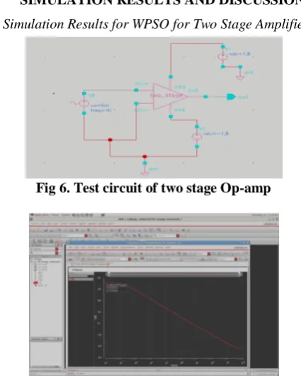
[image:4.595.313.540.51.565.2]4.1 Simulation Results for WPSO for Two Stage Amplifier:
Fig 6. Test circuit of two stage Op-amp
Fig 7: Simulation result of Gain for Two Stage Op-Amp
Fig 8: Power calculation of Two Stage Op-Amp
Fig9: Simulation results of Phase Margin for Two Stage Op-Amp
Fig 10: Simulation results of UGF for Two Stage Op-Amp
[image:4.595.60.273.495.761.2]4.2 Simulation Results of WPSO for Folded Cascode Amplifier
[image:4.595.321.530.568.687.2]International Journal of Innovative Technology and Exploring Engineering (IJITEE) ISSN: 2278-3075, Volume-8, Issue- 6S4, April 2019
Fig 12. Simulation result of Gain for folded cascode Op-amp
[image:5.595.341.511.52.194.2]Fig13. Power calculation of folded cascode Op-amp
Fig 14.Simulation result of Phase Margin and UGF for folded cascode Op-amp
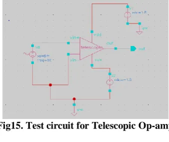
4.3 Simulation Results of WPSO for Telescopic Amplifier:
Fig15. Test circuit for Telescopic Op-amp
Fig 16. Simulation result of Gain for Telescopic Op-amp
Fig 17 Power calculation of telescopic Op-amp
Fig 18. Simulation result of Phase Margin and UGF for Telescopic Op-amp
Parameters
Two stage Folded cascade Telescopic
Specifications Results Specifications Results Specifications Results
Gain 86dB 86.6dB 70dB dB 50dB dB
UGF 5MHz 6.45MHz 100MHz MHz 1GHz MHz
Phase margin
60deg 60deg 60deg Deg 60deg Deg
Slew rate 5V/us 10V/us >100V/us V/us >100V/us V/us
Power <=50uW 63uW <100uW uW <=100uW uW
Area <100um2 97um2 100um2 um2 100um2 um2
[image:5.595.340.513.197.299.2]Fig 19. Layout of two stage operational amplifier
Fig 20. Layout of folded cascode operational amplifier
Fig 21. Layout of telescopic operational amplifier
CONCLUSION:
In this paper, a MPSO based framework is used for the perfect skill of a CMOS intensifier. The cream kind of the atom swarm improvement figuring and weighted system, is proposed to streamline the structure factors, for instance, MOS transistor size, power and meet the given detail. The structure central inspirations driving the CMOS circuits are considered as the cost most distant extents of the Modified Particle swarm movement figuring. The starting outcomes show that the proposed framework possibly meets the circuit structure subtleties what's more inspiration driving restriction the chip check. Regardless of the redirection based structure, the beat virtuoso expansions were done to engage the CMOS to circuit central center interests. It has been demonstrated that the structure of the CMOS circuit using the MPSO approach is advantageous separated and other procedure systems. The proposed system structure can reinforce the CMOS circuit shows up. Beginning now and into the not too expelled the MPSO estimation is a competent point of view for complex key IC structure.
ACKNOWLEDGEMENTS
The makers wish to offer basic thankfulness to JNTU HYD and Anurag Group of Institutions for giving unequivocal workplaces to do this work.
REFERENCES:
1. M. Barros, J. Guilherme, and N. Horta, “Analog circuits
optimization based on evolutionary computation
techniques,” Integr., VLSI J. 43, 136–155 (2010).
2. T. R. Dastidar, P. P. Chakrabarti, and P. Ray, “Synthesis system for analogcircuits based onevolutionary search andtopological reuse,” IEEE Trans.Evol. Comput.9(2), 211–224 (2005).
3. G. G. E. Gielen and R. A. Rutenbar, “Computer-aided design of analog andmixed-signal integrated circuits,”
Proc. IEEE 88(12), 1825–1854 (2000).
4. L. Qian, Z. Bi, D. Zhou, and X. Zeng, “Automated technology migration methodology for mixed-signal circuit based on multistart optimization framework,” IEEE Trans.
VeryLarge Scale Integr. (VLSI) Syst. 23(11), 2595–2605
(2015).
5. T. Levi, N. Lewis, J. Tomas, and S. Renaud, “Application of IP-based analog platforms in the design of neuromimetic integrated circuits,”IEEE Trans. Comput.-Aided Des.
Integr.Circuits Syst. 31(11), 1629–1641(2012).
6. S. H. Yeung, W. S. Chan, K. T. Ng, and K. F. Man, “Computational optimization algorithms for antennas and RF/microwave circuit designs: Anoverview,” IEEE Trans.
Ind. Inf. 8(2), 216–227 (2012).
7. W. Nye, D. C. Riley, A. Sangiovanni-Vincentelli, and A. L. Tits, “DELIGHT.SPICE: An optimization-based system for the design of integrated circuits,” IEEETrans.
Comput.-Aided Des.Integr. Circuits Syst. 7(4),501 (1988).
8. T. McConaghy, P. Palmers, M. Steyaert, and G. G. E.
Gielen, “Trustworthy genetic programming-based
synthesis of analog circuittopologies using hierarchical domain-specific building blocks,” IEEE Trans. Evol.
Comput.15(4), 557–570 (2011).
9. O. B. Kchaou, A. Garbaya, M. Kotti, P. Pereira, M. Fakhfakh, and M. Helena Fino, “Sensitivity aware NSGA-II based Pareto frontGeneration for the optimal sizing of analog circuits,” Integr., VLSI J. 55, 220–226 (2016). 10. A. El Dor, M. Fakhfakh, and P. Siarry, “Multiobjective
differential evolution algorithm using crowding distance for the optimal design of analog circuits,”J. Electr. Syst.
12(3), 612 (2016).
11. M. Dehbashian and M. Maymandi-Nejad, “An enhanced optimization kernel for analog IC design automation using the shrinking circles technique,” Eng. Appl. Artif. Intell.58, 62–78 (2017).
12. S. D. Djordjevic, “Analog circuit sizing using local biasing,” Analog Integr.Circuits Signal Process. 93(2), 299–308 (2017).