Klaus-Peter Zauner
School of Electronics and Computer Science
University of Southampton
Highfield, Southampton, SO17 1BJ
United Kingdom
[email protected]
www.ecs.soton.ac.uk/~kpz/
Manuscript of material that appeared in:
Critical Reviews in Solid State and Material Sciences
,
Volume 30, Number 1, pp. 33–69, 2005.
The article is available from Taylor & Francis at
http://taylorandfrancis.metapress.com/link.asp?id=w375573488537458
ABSTRACT:
Molecular materials are endowed with unique properties of unrivaled potential for high density integration of computing systems. Present applications of molecules range from organic semi-conductor materials for low-cost circuits to genetically modified proteins for commercial imaging equipment. To fully realize the potential of molecules in computation, information processing concepts that relinquish narrow prescriptive control over elementary structures and functions are needed, and self-organizing architectures have to be developed. Investigations into qualitatively new concepts of information processing are underway in the areas of reaction-diffusion comput-ing, self-assembly computcomput-ing, and conformation-based computing. Molecular computing is best considered not as competitor for conventional computing, but as an opportunity for new applica-tions. Microrobotics and bioimmersive computing are among the domains likely to benefit from advances in molecular computing. Progress will depend on both novel computing concepts and innovations in materials. This article reviews current directions in the use of bulk and single molecules for information processing.
KEY WORDS:
polymer electronics, molecular switches, self-assembly computing, conformation-based computa-tion, self-organizing materials, bioimmersive computing
ACRONYMS:
AC—Alternating current ATP—Adenosine triphosphate BR—Bacteriorhodopsin
BZ—Belousov-Zhabotinsky (reaction)
CMOS—Complementary metal oxide semiconductor CPU—Central processing unit
DNA—Deoxyribonucleic acid DRZ—Deoxyribozyme FET—Field effect transistor
FRET—Fluorescence resonance energy transfer LB—Langmuir-Blodgett (film)
LED—Light emitting diode MDH—Malate dehydrogenase
NAND—Negation of logic AND operation NMR—Nuclear magnetic resonance NOR—Negation of logic OR operation NP—Nondeterministic polynomial PCR—Polymerase chain reaction PET—Photoinduced electron transfer RAM—Random access memory RFID—Radio frequency identification RNA—Ribonucleic acid
TTF—Tetrathiafulvalene UV—Ultra violet
TABLE OF CONTENTS
1 Introduction 3
1.1 Scope and Structure . . . 3
1.2 Organic Devices . . . 4
2 Computing Concepts 5 2.1 Current Paradigm . . . 5
2.2 Unconventional Computing . . . 8
3 Implementations 10 3.1 Carbon-based Semiconductors . . . 10
3.1.1 Polymer Electronics . . . 10
3.1.2 Carbon Nanotubes . . . 12
3.2 Molecular Switches . . . 14
3.3 Bacteriorhodopsin: a Photonic Automaton . . . 17
3.4 Excitable Chemical Media . . . 21
3.5 Self-assembly Computing . . . 24
3.6 Conformation-based Computation . . . 30
3.7 Allosterically Regulated Deoxyribozymes . . . 35
3.8 NMR Quantum Computing . . . 36
4 Interfaces, Interconnections, and Architectures 37 4.1 Diffusion and Transport . . . 38
4.2 Uncontrolled Structures . . . 38
4.3 Self-organization . . . 39
5 Perspectives 40
1 INTRODUCTION
1.1 Scope and Structure
A confluence of three research directions brings molecular information technology into focus. The feature size of semiconductor devices [1, 2] is approaching the scale of large macromolecules [3, 4]. The enviable computational capabilities of organisms are increasingly traced to molecular mechanisms [5, 6]. And, techniques to engineer molecular control structures directly into living cells start to emerge [7, 8]. Current attempts to employ molecules for computation fall into two categories. Firstly, investigations aimed at obtaining molecules that mimic components of con-ventional computing devices. Transistors from carbon-based semiconductors and molecular logic gates are examples falling into this category. Secondly, explorations into innovative computation schemes to find information processing concepts suitable for exploiting the special character-istics of molecules. Computation based on reaction-diffusion systems and on self-assembly of macromolecules are in the latter category. The scope of the present review will encompass both of these areas. Nonetheless some fields that are part of molecular information technology have been excluded. Molecules have already found wide spread application in current computing de-vices in two areas, liquid crystals displays and organic dyes in recordable compact disks (CD-R). Both are not covered in the present review. The prospect of molecular computing attracted in-terest from the theoretical computer science community following the publication of Adleman’s experimental work on DNA computing [9] and a considerable body of literature appeared. In a significant part of this, however, abstractions and models have been used that are ill suited to realization. The interested reader will find pointers to the literature in [10]; the present review will focus on realizable computing concepts.
possible in every case. Ribozyme based logic gates, for example, combine aspects of switching, self-assembly and conformational computation all in one single system. Of particular importance for the practical realization of molecular computing devices is the infrastructure to interconnect molecular components into architectures and, in many cases, to interface these molecular archi-tectures with existing information technology; section 4 is dedicated to this aspect. Finally an overview over the challenges and possibilities of molecular computing is offered in the concluding section. In the remaining part of this section the properties of molecules key to their applica-tion and potential in informaapplica-tion technology will be described. The important differences to solid-state technology will also be outlined.
1.2 Organic Devices
The extraordinary diversity of the biological world has its roots in an enormous number of macromolecular structures that implement a wide variety of highly specific functions. These heterogeneous structures are assembled from a small set of molecular building blocks. The building blocks themselves are composed form a limited subset of the elements (mainly H, C, N, O, P, S). Proteins provide a prominent example. In nature these are assembled from 20 types of amino acids (Gesteland [11] lists rare exceptions), which are themselves built up from between 10 and 27 atoms. The amino acids differ in size and shape as well as in their physical and chemical properties. Proteins are linear chains of amino acids linked by covalent chemical bonds. The chains are typically a few hundred amino acids long and their molecular mass corresponds to the equivalent of 10 000 to several million hydrogen atoms [12]. There is no restriction on the order in which the different types of amino acids can occur in the chain and consequently the variety of chains is practically inexhaustible. For proteins only 60 amino acids long and formed from a set of 20 amino acids the number of distinct possibilities (2060) is about as large as the number of atoms in the known universe. A self-organizing folding process maps the combinatorial diversity of possible amino acid sequences into a vast variety of specific functional properties. Proteins thus grant substantial freedom to select specific stimuli to respond to, and to associate these with a response in an essentially arbitrary way.
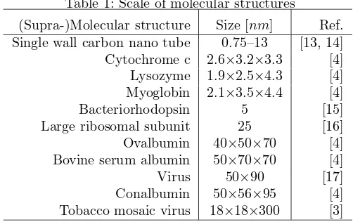
[image:4.595.137.388.480.638.2]Macromolecules have a size that situates them at the interface between micro and macro physics (table 1). They are small enough to exhibit quantum level features and to couple to
Table 1: Scale of molecular structures
(Supra-)Molecular structure Size [nm] Ref. Single wall carbon nano tube 0.75–13 [13, 14] Cytochrome c 2.6×3.2×3.3 [4] Lysozyme 1.9×2.5×4.3 [4] Myoglobin 2.1×3.5×4.4 [4]
Bacteriorhodopsin 5 [15]
Large ribosomal subunit 25 [16]
Ovalbumin 40×50×70 [4]
Bovine serum albumin 50×70×70 [4]
Virus 50×90 [17]
Conalbumin 50×56×95 [4]
Tobacco mosaic virus 18×18×300 [3]
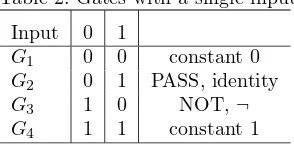
Table 2: Gates with a single input
Input 0 1
G1 0 0 constant 0
G2 0 1 PASS, identity
G3 1 0 NOT,¬
G4 1 1 constant 1
From an information processing perspective the keenly discriminating specificity of macro-molecular interaction entails a marvelous pattern recognition capacity [32, 33] that supports computing based on the self-assembly of molecular data representations [34, 35]. In the past decade the practicality of such and approach has been demonstrated for minimal problem in-stances with self-assembly of short deoxyribonucleic acid (DNA) strands [9, 36].
Another route to molecular computing is based on the flexibility of macromolecular structures. Changes in the conformation, i.e., changes in the spatial positions of the atoms of a molecule that do not require disruption of covalent bonds, can be used to store and to process information. The protein bacteriorhodpsin is a particularly successful example of the application of this principle (c.f. sections 3.3 and 3.6). Part of the success of this protein can be attributed to its stability. It is worth pointing out, that the existence of a ground state and discrete energy levels insure that multiple copies of a molecule have and maintain identical properties. A water molecule, for example, that is a million years old is indistinguishable from a water molecule produced a millisecond ago. Fatigue or wear out as may be found in macroscopic structures [37] does not exist for individual molecules. Their parameters are constant throughout lifetime and thus enable the implementation of computation methods exploiting the subtle intricacy of molecular response [38].
Within the field of molecular electronics the development of polymer conductors and semi-conductors formed a focus point early on [39, 40, 41]. Initial predictions that polymer circuits would arrive within 20 years [42] turned out to be quite accurate, although the advantage of the circuits that are within reach now [43, 44, 45] is not, as had been hoped, integration den-sity and speed, but reduced fabrication cost per circuit—but not per transistor—as compared to conventional silicon-based circuits. The most immediate widespread application of molecular information technology is likely to arise from the use of low cost, low performance polymer cir-cuits in ubiquitous computing. In these applications, so far, molecular materials are enlisted to implement essentially standard logic circuits.
2 COMPUTING CONCEPTS
2.1 Current Paradigm
The idea of a computing machine was conceived with the desire to free the mind from tedious, repetitious calculations as they occurred in the preparation of, e.g., astronomic and trigonomet-ric tables. Before computers took over routine calculations, the methodology for performing these was based on standardized forms for collecting intermediate results and for tracking the incremental progress of the computation. The architecture and operation of current computers directly corresponds to this methodology.
Table 3: Common logic gates with two input lines
Input A 1 1 0 0 Implementation
Input B 1 0 1 0 Sym. with NAND with NOR
NOT 0 0 1 1 ¬ A|A A5A
AND 1 0 0 0 ∧,· (A|B)|(A|B) (A5A)5(B5B) OR 1 1 1 0 ∨, + (A|A)|(B|B) (A5B)5(A5B)
XOR 0 1 1 0 ⊕
NAND 0 1 1 1 |
NOR 0 0 0 1 5
COMP 1 0 0 1 ≡
four possible gates with a single input line, there exit 16 gates with two input lines. Again some of these ignore all or one of the inputs, and only the logic operations shown in the six lower rows of table 3 are in practice useful. Combinations of logic gates can operate on more input lines. For example two AND gates can be combined to form an AND with three input lines (I1, I2, I3), by first applying an AND gate to I1 and I2 and then applying and AND gate to the output of the first gate and I3.
A suitably chosen subset of the logic gates shown in tables 2 and 3 is sufficient to express arbitrary logic relationship between input variables. Such a set of gates (or logic operations) is called universal. An example of a universal set is the combination of NOT, AND and OR. To elucidate how this set of operations can implement an arbitrary logic function, one can imagine a table in which the nleftmost columns represent the states ofninput variables. According to the 2n
possible state combinations of the input variables there would be 2n
rows in the table. A further column at the right would assign to each of the rows an output value. For simplicity of the present explanation (but without loss of generality) a single output line may be assumed. The filled-in table defines a logic gate withn input lines and one output line. To compose this logic gate from the universal set mentioned above, it is sufficient to consider only rows for which the output is 1. For each such row one employs NOT gates to invert any input signal that is in a zero state. One then combines the input lines and the inverted input lines with a cascade of AND gates. The output line of the final AND gate in the cascade is the output for the row and will be in a 1 state only if all input variables are in the state indicated by the corresponding row in the table. Finally the outputs of all 2n
rows are combined in a cascade of OR gates. The output of the final OR gate is the output for the logic function defined by the table. While the resulting circuit may not be the smallest possible, the construction illustrates that NOT, AND and OR gates can be combined to implement any arbitrary logic function, and shows that this set of gates is universal. It is possible to construct each of the three gates NOT, AND, and OR from NAND gates alone, and it is also possible o construct the three gates using only NOR gates, as indicated in the two rightmost columns in table 3. Consequently the NAND gate alone is sufficient to implement any other logic function, it is a universal gate. Also the NOR gate is universal.
To combine the gates into circuits two further building blocks will be required: a fanout element and an exchange element. The former replicates a single input line on two output lines, the latter exchanges the signal between two lines or two storage locations. In electronic implementations the former may just be a forking connector and the latter could be the crossing of two isolated connectors. Both are often implicitly assumed, but it is important to be aware of them for unconventional implementations [47]. If, for example, a signal is represented by a molecule instead of an electrical potential then the fanout element may need to replicate the molecule.
chain of PASS gates will act as a delay line and temporarily retain the state of a previous input. As a consequence the output of a network of gates may not be solely a function of the input variables, but can also depend on the internal state of the network and thus on the history of inputs [49].
If the states of the network are discrete and the network consists of a finite number of com-ponents, then the network can only assume a finite number of states. Accordingly the network can only distinguish among a finite number of input histories. Such a processor is called a finite state automaton and is typically represented as a graph. The nodes in the graph correspond to states of the processor and the edges correspond to state transitions caused by input signals [50, 51]. Any realizable digital computer is a finite state automaton, although often with a vast number of states.
The success of digital electronic circuits in implementing such automata has been attributed to several key factors common to relays, vacuum tubes, and transistor technology [52]:
• Tolerance to variation in component parameters arising from production, aging or environ-mental effects
• Resilience with regard to signal degradation and noise
• Restoration of output through high gain
• Ability to interconnect
It is interesting to note that historically the speed of individual components was not as important for the success of a particular technology as low power dissipation. The latter permitted high integration density and thus provided better overall system performance based on the slower components [53]. The scaling of electronic logic devices proceeded fairly predictable for the past 30 years with an essentially unchanged operational principle and device structure, and another decade of scaling seems physically feasible, although the economic limit of scaling may be closer [54, 55].
Computers excel in the tasks for which their concept was originally intended. Nevertheless many interesting information processing problems appear to be out of reach of our current computing devices. The ultimate limitations of computing have been discussed from theoretical and physical perspectives. At the heart of the study of theoretical limits on computability lies the notion of ‘effective computation’. An effective computation can be carried out by a machine that executes precise instructions without any need for intuition, innovation, or guessing.
Turing [56] suggested a machine model that essentially comprises a finite state automaton coupled to an unlimited memory and permitted to operate without time restriction. This model has been shown to be equivalent to several independent formulations of effective computation by Church, Kleene, Post, and others [57]. It is now generally believed that all formulations of effective computation are equivalent and that anything that in principle can be computed can also be computed on Turing’s machine. A machine capable of carrying out any computation is called a universal machine. Such machines are hypothetical constructs, because they cannot be limited by finite memory. The central result in computability theory is the proof that problems do exist that cannot be computed on a universal machine despite its unlimited resources. It is worth noting that universal machines can be surprisingly simple. Minsky offers a Turing machine design with a seven-state finite state automaton. Similarly a processor with a unlimited random access memory (RAM) needs an instruction set of only two instructions (‘increment’ and ‘decrement with conditional jump’) to be capable of computing anything that is computable [50].
With this in mind it does not come as a surprise that even the early computing devices were finite memory approximations of universal machines. This universality led to many new directions of application. The all-purpose character of the computer together with the steady advance on the limits of memory space and CPU time shielded the underlying computing concept from challenge, and technological progress focused on quantitative improvements.
of mathematics into physical reality. The border is crossed in the strong version of the Church-Turing Thesis that can be stated as: any real-world process is effectively computable. A corollary is, that no physically realizable system (e.g., the human brain) can compute anything that could not in principle be computed on the present day computers, given enough memory and time.
The comparative capabilities of actually realizable systems shows a picture quite different from that yielded by a comparison of the ultimate theoretical limitations of their concepts. If effective computation is identified with physically realizable dynamics, then computability becomes constrained by physics. The velocity of light is the ceiling for the distribution of signals. Heisenberg’s uncertainty principle limits the speed with which system states represented by energy differences can be determined. The physical upper bound on the amount of information processed within one second by a processor with a mass of 1 g has been calculated by Bremermann [59, 60, 61] to be about 2×1047 bit.
Physical limitations on computation arise also from the need to represent information by physical degrees of freedom and the resulting thermodynamic effects caused in the course of computation [37]. Instead of imposing a predefined logic behavior on the dynamics of the com-puting system, the course of computation can be driven by physics itself [35]. If the strong Church-Turing Thesis does hold, the class of problems that can be solved in principle with com-putation driven by physics will be the same as the class of problems that can be solved with formal systems. Then, in principle, every computable problem can be solved some day using the conventional computing paradigm, assuming open ended increase in memory capacity and processing speed [50]. But this does not mean that the current kind of computing is the suitable tool for all information processing problems. In application areas that do not resemble the cal-culation of tables, present-day computers have a hard time exhibiting satisfactory performance. Do alternatives exist?
2.2 Unconventional Computing
With the prevailing success of the common general purpose computer information processing became almost synonymous with digital computing. During the early days of computer science, however, the term ‘computer’ referred to a wide range of information processors [62], ranging from mechanical function generators to hydraulic equation solvers, and included human beings [63]. For the consideration of qualitatively new types of information processing devices it is helpful to return to this broad view of computing: A computer is a system that starts from a state which encodes a problem specification and changes, following the laws of nature, to a state interpretable as the solution to the problem [64]. Following this definition, a system trivially computes its own behavior. Any physical dynamics can usefully be employed for information processing if an interpretation is found to transcend the question of the system’s own behavior. The physical dynamics can be carefully tailored to closely adhere to a formal model of computation. The engineered constraints in the electrodynamics of the common digital computer are a case in point. Or the physical dynamics can be used in a direct way by selecting encodings and interpretations. The use of a lens to implement a Fourier transform is an example. The latter approach often provides a simple implementation for an intricate input-output mapping. This, however, comes at the price of narrowing the application domain [65]. Developing concepts of computation that do not impose such rigid constraints on the physical dynamics of the implementation as to abrogate its efficiency [66], yet are flexible enough to be of general use is a challenge. In the context of molecular information processing the search is for paradigms capable of exploiting the specific characteristics of molecules rather than requiring the molecules to conform to a given formal specification.
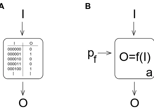
O
I
I O
... ...
f
p
000000 000001 000010 000011 000100
0 1 0 0 1
a
I
B
A
[image:9.595.140.391.82.259.2]O
O=f(I)
Figure 1: Communicating a desired input-output map to a machine. The input-output map can in principle be thought of as a potentially very large lookup table that associates an output response with every input that can be discerned by the machine (A). Fornbit input patternsIand ambit output(O) response the, number of possible maps is 2m2n
. To implement an arbitrary one of these maps on a quasi-universal machine, the mapping
f has to be specified by the program p with respect of machine architecture a (B). Selecting an arbitrary map from the set of possible maps may require a specification of length: log2
£ 2m2n
¤ =m2n
. Even for moderate pattern recognition problems (e.g., classifying low resolution images) the program length required for most mappings is impractical [38, 73].
cellular automata computing. However, concepts for massively parallel computing inspired by the self-organized collaboration of biological cells in organisms are under development. Amor-phous computing, for example, assumes a large number of identically programmed computing devices in arbitrary positions and orientations. The computing devices interact through short range communication and are explicitly assumed to be unreliable [70]. This concept relaxes two constraints imposed by conventional computing architectures. The components do not have to be arranged following exactly a predetermined spatial structure and the components do not all need to perform according to narrow specifications. The amorphous computing concept is an important step towards broadening the material basis of computation to include molecular and nano materials. However, it does suppose that the elementary devices are programmable and global functionality emerges from handmade programs executed by the elementary devices. This assumption limits the efficiency as well as the general usability of the inherent parallelism [71, 72].
One way to overcome this problem would be specialized hardware with only a limited applica-tion domain. In the extreme case it may be useful to build an instance machine, i.e., a specialized computer architecture dedicated to solving a single problem instance. This opens up several de-sign degrees of freedom [77]. In particular the upper bounds for the number of state transitions individual components have to support can be very low. Materials and procedures that would not come under consideration for conventional computing devices may find niche applications in instance machines.
Another way for implementing complex input-output maps is to avoid programming. Pro-grammability is not a prerequisite for the realization of information processing systems as is exemplified by the enviable computing capabilities of cells and organisms. Artificial neural net-works provide a technological example of non-programmed information processing [72]. They trade an effective loss of programmability for parallel operation. This approach could be taken much further, however. As programmability has essentially been relinquished, the individual net-work nodes do not need to perform identically. Inhomogeneity and context-sensitive components can be introduced to increase the computational power and the efficiency the network [66, 78]. These steps abrogate present training algorithms for artificial neural networks. At the same time however, the increased dimensionality enhances the evolvability of such networks. The evolu-tionary paradigm of using the performance of an existing system as an estimate for the expected performance of an arbitrarily modified version of the system can cope with the complexity and inhomogeneity of architectures based on context sensitive components. In fact it is particularly effective in this domain [79].
In general, however, evolving highly complex input-output maps from scratch may take so long as to be impractical. It is here where the concept of ‘informed matter’ [80], i.e., molecules delib-erately designed to carry information that enables them to interact individually, autonomously with other molecules, comes into play. Already the level of reaction kinetics supports considerable computational capabilities [81] and fast algorithms for simulating kinetic computing schemes are available [82]. Abstract concepts in artifical chemistry [83] go beyond the kinetic level and encom-pass supramolecular interactions. The developments in supramolecular chemistry [84, 3, 80] point towards the possibility of implementing computing schemes developed as artificial chemistries with bona fide molecules. Conceivably this will enable orchestrated self-organization to arrive at time scales that is practical and thus enable physics driven architectures.
3 IMPLEMENTATIONS
3.1 Carbon-based Semiconductors
3.1.1 Polymer Electronics
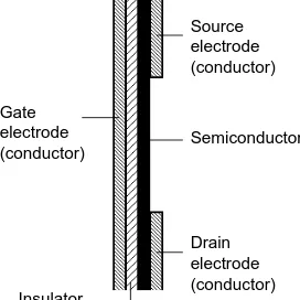
Current information processing devices are generally based on networks of electronically actuated switches. The type of switch most commonly employed is a variant of the field effect transistor (FET) first described by Shockley [85]. Fig. 2 depicts a typical configuration of an insulated gate FET. If the electric potential at the gate electrode is zero, the current flow between source and drain electrodes is low. On application of a potential at the gate electrode, a charge is induced at the insulator-semiconductor interface. The charge provides carriers in the semiconductor layer and enables an increased current flow between the source and drain electrode. Consequently the gate can be used to switch the source-drain current on and off. The characteristics of the transistor can be modified by altering the geometry of the gate. In conventional FETs the insulating layer can be formed by metal oxide that separates the gate electrode from an inorganic semiconductor such as Si, a technology known as metal-oxide semiconductor (MOS).
Within two decades of the demonstration that an organic polymer (polyacetylene) can also serve as semiconductor in a FET [86, 87] carbon-based FETs have reached the verge of commer-cialization [88]. However, due to their low mobility (i.e., charge carrier velocity per unit electric field) they cannot compete with the speed of inorganic semiconductor switches. It has been sug-gested that low mobility could potentially be overcome by reducing the organic semiconducting layer to a single macromolecule [88]; thus eliminating the need for charges to hop from molecule to molecule while traveling between source and drain.
Source electrode (conductor)
Drain electrode (conductor) Gate
electrode
(conductor) Semiconductor
[image:11.595.194.330.97.233.2]Insulator
Figure 2: Conducting, semiconducting and insulating materials are required to assemble an in-sulated gate FET, but the configuration is relative simple and well suited for low-cost production.
hypothetical molecule consisting of an electron donor part connected by a saturated (σ-) bridge to an electron acceptor would function as a single-molecule diode [25].
Rectification has been achieved in a multilayer stack of oriented molecules [90] that was pre-pared by the Langmuir-Blodgett (LB) technique [91, 92]. Subsequently a LB monolayer acting as photodiode was obtained [93]. This result indicated that single molecule devices are indeed realizable. The synthesis of a molecule that acts as a rectifier, however, turned out to be far more arduous than what had been anticipated and an unimolecular rectifier was achieved only recently [94, 95]. Rectifiers suffice to implement logic AND and OR gates [96]. But, as noted in section 2, for implementing the complete set of logic functions, inverters are required in addition to AND and OR gates. Simulations suggest that individual Fullerene (C60) molecules could potentially be used to build inverters and furthermore that the NOR operation may possibly be implemented with two C60molecules [97]. NOR gates alone would allow for the realization of all logic functions as can be seen from the rightmost column of Table 3. Here may be mentioned that C60is of interest not only for single molecule devices but also in bulk as n-channel semiconductor material, [98] especially because most known organic semiconductors are p-channel materials.
The rising commercial interest in molecular electronic devices focuses currently on the use of bulk material, not individual molecules. Slow switching speed concomitant with the use of bulk organic materials are offset by the potential for low-cost fabrication, large circuit area, mechanical flexibility, light weight, and production processes compatible with temperature sen-sitive materials such as transparent plastics. To realize these possibilities, ideally all layers of the FETs (cf. Fig. 2) should be implemented with molecular materials. Recently de Leeuw and co-workers showed that this is feasible by building integrated circuits in which the insulating, conducting and semiconducting layers are polymers [43]. These circuits comprise several hundred FETs connected as 15-bit programmable code generators. Versions fabricated with pentacene as semiconductor are reported to operate at up to 100 bit/s and to show negligible performance loss after exposure to air for over a month [44]. The latter is encouraging since many organic semiconductors with otherwise interesting properties degrade in the presence of oxygen through oxygen-doping and oxidation. Encapsulation of the circuits may in principle be used for ob-taining reliable devices with adequate shelf and operational life time. For low-cost fabrication, however, it would be desirable to have organic materials available that are not overly sensitive to open air and impurities.
Solubility is another property sought in organic semiconductors. Solution-processable mate-rials which can be patterned by printing and printing techniques are ideal to facilitate cheap production [99, 100, 101, 102]. The demonstration [45] of a ring-oscillator produced from solu-ble polymers that is capasolu-ble of operating at 106 kHz is therefore a significant step toward the commercial application of organic FETs.
+V
Gnd
In Out
p-channel Transistor
[image:12.595.199.336.89.245.2]n-channel Transistor
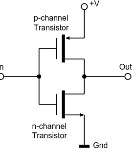
Figure 3: Logic NOT (inverter) in CMOS technology. Power is only consumed during a state change, since for both input states (high and low) only one of the two transistors will be conducting.
fabricated with photolithographic patterning [104]; achieving the same with printable materials is highly desirable to allow of low cost power supply options. We note however, that the low power consumption of complementary circuits is largely due to the small number of gates that are active at any given point in time (see section 2 above). Architectures that rely on concurrent operation of the active elements would considerably reduce the CMOS advantage.
A strong drive for the commercial development of polymer-electronic is the immediate and potentially very large market for radio frequency identification (RFID) [105]. Transponder tags for RFID are comprised of an antenna and a low complexity circuit that is powered by incoming radio waves. Upon activation the circuit broadcasts a unique identification code that can be matched to a database to track the movement of the tag in space and time. Cheap circuits of sufficient speed to operate at the established RFID frequencies would make the automatic identification of low cost items economically viable. The performance limitation of organic semi-conductors are addressed not only by seeking new materials, but also with new circuit designs. Baude et al. proposed an AC powered inverter, thus eliminating the need for a high quality rectifier component [106]. They demonstrated a pentacene-based implementation of an AC pow-ered 7-stage ring-oscillator, but with only 1 bit modulation [107]. It remains to be seen whether identification codes with a useful bit length can be implemented with the AC powered design. Undoubtedly, the adaptation of the circuit design to the specific properties and limitations of the materials is a promising path.
The potential advantage of low-cost, large circuit area and fabrication methods compatible with heat sensitive materials indicate a promising future for organic electronics. Current research fo-cuses on utilizing the large circuit area and low processing temperatures (suitable for flexible and transparent plastics) in displays [108]. It appears likely that these features will also enable numer-ous biomedical and biotechnology applications based on integrating organic electronic circuitry with biomolecules and even micro organisms [109, 110]. The shelf-life and operation time of such bio-electronic hybrid systems may be limited by the integrated bio-compounds or cells and thus offer a niche application in which materials with limited stability can usefully be employed.
3.1.2 Carbon Nanotubes
Si
SiO
Pt
CNT
Pt
[image:13.595.149.378.87.210.2]2
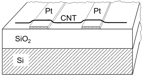
Figure 4: Carbon nanotube field effect transistor. A single walled semiconducting carbon nan-otube (CNT) contacts two platin electrodes (Pt). A semiconducting Si substrate serves as gate electrode insulated from the platin electrodes and the CNT by 300 nm of SiO2. This thick insulating layer results in less than unit gain (0.35). The insulating layer can be reduced to a few nm, permitting about unit gain. After [114].
of several µm is typical [13, 14]. A slight longitudinal shift can be introduced when matching the dangling bonds along the edges and will cause a helical twist in hexagonal lattice of the tube walls. Depending on diameter and on the degree of helicity the electronic properties of the tubes can vary from conducting to semiconducting [113].
Tans et al. demonstrated a FET based on a single-walled semiconducting carbon nanotube [114]. The device, illustrated in Fig. 4, operates at room temperature and a conductance change of about six orders of magnitude for a gate potential of 10 V was reported. The contact resistance, however, was high and a resistance of 1 MΩ was measured for the conducting state. Furthermore the gain of this transistor was below unity and hence the transistor would not be suitable in circuits where it would need to drive other transistors.
As mentioned above, carbon nanotubes can be pictured as rolled hexagonal lattices. The end caps however do contain six pentagons among the hexagons [13]. Owing to the higher reactivity of pentagons compared to hexagons the end caps of nanotubes can be destroyed by oxidation. This provides free bonds on the nanotube ends that can be functionalized by covalently linking the tube to another molecule. It is possible, for example, to link nanotubes to single stranded DNA [115, 116]. The self-assembly properties of complementary DNA strands, further discussed in sections 3.5 and 4.3, can then be exploited for attaching the DNA-functionalized nanotube at a specific location of a solid support or for attaching the nanotube to other molecules, including other nanotubes. Particularly attractive are noncovalent methods of attaching macromolecules to single-walled carbon nanotubes, because these methods leave the extended electronic structure of tubes intact. Noncovalent binding can be accomplished by wrapping of the tubes [117] or by using a highly aromatic linker that adsorbs irreversibly onto the hydrophobic surface of the tubes [118, 117].
Keren et al. devised an original strategy to form electric contacts with a carbon nanotube [119]. They self-assembled a semiconducting nanotube in the center of a 16 µm DNA molecule. The DNA molecule was then coated with gold except for some area along the tube which was protected by a DNA binding protein. They used this assembly to implement a nanotube FET similar to the type shown in Figure 4, but with the DNA-templated gold wire replacing the platinum contacts on either side of the nanotube which is itself bound to the DNA molecule.
Dekker and co-workers found that nanotube FETs with an on-off ration of≥105and a gain of 10 can be achieved by using a microfabricated aluminum wire as gate electrode which is insulated from the nanotube by its native layer of Al2O3[120]. These transistors are of sufficient quality to permit multi-transistor circuits. Circuits with up to three nanotube FETs have been produced, including the universal NOR gate (cf. table 3), a two-inverter flip-flop as 1 bit static memory cell, and a three-inverter ring-oscillator (cf. section 2.1).
con-tact resistance and the formation of multi-device circuits without a need for positioning each individual nanotube manually. The possibility to functionalize carbon nanotubes with macro-molecules raises the prospect of tubes with new and tailored characteristic becoming available. The excellent reviews of Ajayan [13] and Terrones [14] are recommended for further information.
3.2 Molecular Switches
The quest for molecular transistors discussed in the previous section is largely driven by their potential as building blocks for switches. It may be recalled (from section 2) that current com-puting technology is build on vast networks of simple switches that implement logic operations as well as memory. Direct realization of a high-quality molecular switch rather than through interconnection of molecular transistors is therefore an attractive idea. Early considerations of switching in molecular systems showed that bistable kinetics can be realized with bulk chemical reactions [23]. In this section, however, the focus is on individual molecules or supramolecular systems that can act as switches.
If a very large number of switches is available and can be suitably connected then even a switch that sustains only a single switching cycle may be of technical interest. Such devices could be used to store input-output mappings in enormous lookup tables, essentially replacing active computation with a vast amount of memory.
A molecular switch that can be opened irreversibly has been demonstrated with rotaxane molecules [123]. The rotaxane comprises two motives, a molecular ring and a v-shaped molecule. The ring is interlocked with one arm of the v. Large molecular groups cap the ends of both arms of the v-shaped molecule and prevent the ring from sliding off. A monolayer of these rotaxane molecules was sandwiched between two electrodes (terminal–Al/Al2O3—C—Ti/Al–ground). At a bias voltage below -1 V the device is conducting. A positive bias of 0.7.–0.9 V leads to oxidation of the rotaxane and permanently opens the switch. Diode-type [124, 125] AND gates and OR gates, and write once configuration by irreversible switching have been reported [123].
Reversible redox-controlled switches have also been developed [126]. [2]Catenanes are molecules comprised of two interlocked molecular rings. Oxidation of a [2]catenane molecule results in a rotation of one of the rings relative to the other (Fig. 5 A) and yields a conducting state. The catenane can be reset to the open-switch conformation by applying a reducing potential. How-ever, the switching effect in the [2]catenanes is less pronounced than in the irreversible rotaxanes. Pseudorotaxanes, a family of molecules where the two sliding molecular motives are not inter-locked, but self-assemble may point a way to more effective reversible molecular switches (Fig. 5 B).
The researches of Tour and collaborators appeared to indicate that conjugated phenylene ethynylene oligomer derivatives can serve as conductance switches in electronic circuits [127, 128]. Theoretical analysis attributed the observed negative differential resistance of the molecules to electron adsorption [129]. On account of the conductance switching in molecules individually addressed by means of scanning tunneling microscopy it has been concluded that the switching is not an electrostatic effect of charge transfer, but due to conformational switching in the molecule [130]. Measurements taken on individual molecules insulated by inserting in a self-assembled alkanethiol monolayer confirm a negative differential resistance for single molecules [131].
In the light of a recent observation that switching behavior can occur in some experiments even in the absence of molecules, [132] the work on conductance switching with phenylene ethynylene oligomers appears at present controversial. Perhaps, electromigration of contact metal first forms conducting nano filaments at low voltages and these then break at higher voltages [132]. It remains to be seen to what degree contact effects, electromigration, metal filaments, or other artefacts have affected the experiments on molecular electronic switching that have been reported in the literature.
+ +
+ +
Red Ox
+ + +
+
+ +
+ +
+ +
+ +
+ +
TTF TTF
TTF
e− e−
A
B
[image:15.595.145.386.84.286.2]+ +
Figure 5: Bistable molecules can function as redox-controlled molecular switches. The left panel (A) shows the two interlocking rings of a [2]catenane molecule schematically. A pos-itive voltage bias oxidizes a tetrathiafulvalene group (TTF) in the crown ether ring of the [2]catenane molecule. Electrostatic repulsion rotates the crown ether ring and closes the switch (bottom). Removal of the voltage bias will reduce the TTF. The [2]catenane molecule, however, will stay in the closed-switch conformation. A nega-tive bias is required to return the crown ether to its open-switch position (top). Solid state switches have been prepared from the [2]catenane and the currents in the open and closed state were found to differ by factor of about three [126]. A supramolecular pseudorotaxane based on the same molecular motifs as the [2]catenane is schematically shown in panel (B). A positive bias ionizes the TTF group, whereupon Coulomb forces drive a reversible shift between the two molecular components. The pseudorotaxane exhibits a sharp change in conductance and hysteresis characteristics that indicate the potential to fabricate improved solid state switches. After [126].
Thermal energy or again irradiation with light returns the molecule to its thermodynamically stable state. By means of the different absorption of the two states it is possible to optically read out the state of the molecule. The next section presents an example for photochromism in more detail.
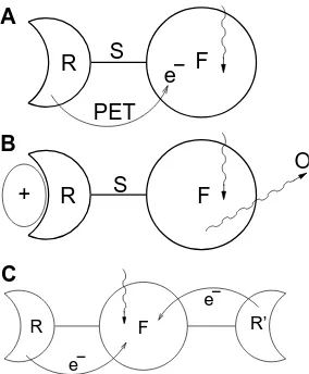
Optical output from molecules does not need to be conveyed by a change in the molecule’s absorption. Fluorescence is an attractive option, because it can be quenched very effectively and thus affords large on-off signal ratios. The quenching of a fluorophore can be achieved photochemically through transfer of an electron to or from the fluorophore. The photoinduced electron transfer (PET) process that turns off the fluorophore can be affected by the chemical environment of the group that provides (or accepts) the transferred electron. This principle underlies a series of molecular switches that can be pictured as consisting of three modules, a receptor, a spacer and a fluorophore [137]. A fluorescent AND logic gate with chemical input signals in form of sodium and proton ions was devised along these lines [138]. Figure 6 illustrates the concept. The modular construction of theses molecules provides considerable freedom for design. Fluorophores can be chosen according to desired excitation and emission wavelength and receptors can be adapted to the input signals. By now the collection of available fluorescent switches includes XOR, NAND and NOR gates among more idiosyncratic logic tables [139].
+
e−
e− F
R R’
e−
S F
R
R S F
A
B
C
PET
[image:16.595.194.336.85.257.2]O
Figure 6: Molecular fluorescent switch comprised of a receptor (R), spacer (S) and fluorophore (F). Photoinduced electron transfer (PET) from the unoccupied receptor quenches the fluorophore, the switch is off; panel A. A cation signal (+) bound to the receptor prevents the PET and a fluorescence signal is emitted, the switch in on; panel B. If two receptor modules are coupled to a fluorophore the molecule behaves like a logic AND gate. Only if both receptors are occupied the electron transfer to the fluorophore ceases and a fluorescence signal appears. After [137].
In the fluorescence switches discussed above electrostatic influences on the receptor biased the competition between fluorescence and PET. Another mechanism for turning the quenching of a fluorophore on and off would be to change the spatial separation between fluorophore and quencher. Some biological macromolecules undergo large but well defined change in shape in response to interaction with other molecules or ions. By judiciously linking a fluorescent dye and a quencher to such a macromolecule the conformational change can give rise to an optical output signal. The folding of self-complementary DNA and RNA single strands is among the most predictable conformational changes in large macromolecules. A strand in which the nucleotides at one end are complementary to the nucleotides at the other end will form a hairpin like structure in which the two complimentary ends are aligned. (Fore more detail on the self-assembly of DNA strands see section 3.5.)
Tyagi and Kramer attached on one end of a partially self-complimentary DNA strand a flu-orophore and on the other end a quencher [141]. The resulting molecular beacon folds into the hairpin structure and by so bringing the quencher and fluorophore moieties close together turns its own fluorescence off. If this molecular beacon encounters a single stranded DNA molecule that contains (or consists of) a sequence complementary to the beacon’s sequence then the beacon opens and fluorescence is turned on (Fig. 7).
cs
cs
F
Q
cs
T
F
cs
Q
B
T
[image:17.595.192.333.86.288.2]A
Figure 7: Molecular beacons signal the recognition of a specific DNA or RNA sequence [141]. The beacon consists of a piece of single stranded DNA with a sequence part at one end (cs) being complementary to the corresponding part ( ¯cs) at the other end. The two complementary sequences surround a sequence ( ¯T) complementary to the target sequence to be recognized. One end of the sequence carries a fluorophore (F), the other end a quencher (Q). The DNA strand folds unto itself and prevents fluorescence by bringing the quencher close to the fluorophore; panel A. Binding of a DNA strand containing the target sequence (T) opens the beacon and separates the quencher from the fluorophore. The latter optically indicates the binding of the target sequence; panel (B).
regulation and electric signaling, for example, for the generation and propagation of action potentials in neurons [146, 147].
Molecular switches play an important part in gene regulation networks and can be used to turn the transcription of genes on or off [7, 8]. Overlapping protein binding sites on DNA have been suggested for the realization of flip-flop switches that would result in sharp on-off transitions [148]. The cellular response to switching in gene networks is intrinsically slow and is not a path for advancing computing power. But it is of value as a research tool for experimenting with dynamically modulated gene expression [8] and harbors great potential for applications controlling individual cells. The latter could be used, for example, to orchestrate microbes in environmental restoration tasks or to activate the production of a drug when a need for it is sensed by a combination of sensors. A step in this direction is described in section 3.7.
A problem of optical molecular switches is that the photo excitation required to read the switch state can lead to side reactions and therefore has the potential to alter to the molecule. Let us proceed now to a molecule that has proved to be exceptionally stable in this regard.
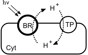
3.3 Bacteriorhodopsin: a Photonic Automaton
248-amino-Cyt
TP
H
+
BR
h
ν
[image:18.595.181.352.91.198.2]H
+
Figure 8: The protein bacteriorhodopsin (BR) is found in the cell membrane of Halobacterium salinarium. It functions as a light-driven pump, moving protons from the cytoplasm (Cyt) to the extracellular space. Thus, BR transduces light energy (hν) into an elec-trochemical potential in form of a proton gradient across the cell membrane. This potential then powers transmembrane proteins (TP) that synthesize ATP (the ‘energy currency’ of cells) or serve as ion pumps.
acids protein, BR, serves as a simple, efficient, and robust solar power source (Fig. 8). BR uses light energy to pump protons from the inside of the bacterium across the membrane to the extra-cellular space. Thus it generates an electro chemical potential across the cell membrane which in turn is used as a driving force for various transmembrane proteins. A photocycle (i.e., a pumping cycle) takes 10 ms and comprises a series of conformation changes of the protein. At least eight conformation states can be identified in the physiological photocycle, more if non-physiological conditions are taken into account [152]. Absorption of light by a chromophore located in the interior of BR initiates the photocycle. The first conformation change, the isomerization of the chromophore, is reported [153] to take 500 fs. It is followed by a sequence of BR states, each with a characteristic spectrum and state life time [154].
Conformational states with distinct absorption maxima in combination with the possibility of photonic state switching are the basis for BR’s great technical potential. Fig. 9 depicts conformation states and photo inducible transitions that are particularly relevant for information processing and storage applications. The large spectral shift for B↔M transitions of≈160 nm, and state switching with wavelengths in the visual light range are notable. BR is at the same time highly photosensitive (the quantum efficiency for both the B→M transition triggered with green light and the M→B transition triggered with blue light is above 60%) and exceptionally stable against thermal, chemical and optical degradation. In combination these features are unrivaled by any synthetic material [156]. Of great importance for technical applications is the exceptional stability of BR. Hampp’s group found that BR films can undergo over a million switching cycles and consequently are well suited for real-time optical computing at video frame rate [15]. The very fast initial conformation change of BR permits optical recording on picosecond time scale. Furthermore, BR films support an optical resolution in excess of 5000 lp/mm and are routinely fabricated with over 80 cm2 apertures [155].
The BR molecule has been studied extensively for over thirty years both from the perspective of its physiological function and also as material for technical applications [158, 155]. Optimized over billions of years by natural evolution BR exhibits characteristics of what has been termed an ‘intelligent material’. As a single molecule it integrates the ability to sense environmental conditions, to process the sensory information, and to adapt its function accordingly [159].
B
570nm
M
409nm
O
640nm
P
490nm
Q
380nm
kT
kT
kT
630-700nm 430-530nm
520-640nm
400-430nm
yellow purple
[image:19.595.165.369.90.244.2]blue pink
Figure 9: Transition scheme for BR states commonly used in information processing experiments. Circles represent spectroscopically identifiable states of the BR molecule. Characters in the circles show the (traditional) names of the states; the peak absorbance wavelength of each state is given below its name. A color name next to a state indicates the appearance of bulk BR in that state. Thermal transitions (kT) are shown with straight arrows, photonic transitions are drawn with bend arrows. The latter are labeled with the wavelength range suitable to induce the transition. States P and Q are not occupied under physiological conditions. The photoinduced B↔M transition comprises a series of three intermediate states (not shown) and takes place in ≈50 µs. The M state facilitates the proton pumping. Under physiological conditions the thermal M→O→B transition will take place in a few ms. Several techniques have been developed to delay the M→O transition for short and long term storage. Note that the wavelengths can shift several 10 nm with changes in the physiochemical conditions of the BR film. Compiled from references [155, 156, 157].
genetic variant, BR-D85N (the corresponding substitution at position 85) provides access to the non-physiological states P and Q (Fig. 9) under moderate conditions; in wild-type BR states P and Q are only available at low pH or through deionization [155].
Besides photochromic switching, BR exhibits a photoelectric effect [163]. Technical use of the latter is more challenging than of the former because it requires the preparation of films with highly oriented BR molecules. Nevertheless the possibility to interface BR electrically is the basis for several suggested applications. The use of BR in optical sensors for acquiring and low-level processing of the input signal [164, 165, 166], and the BR-based optically reprogrammable artifi-cial neural network design [167, 168] illustrated in Fig. 10, are examples. Photoelectric properties of BR have been altered with the introduction of chemical analogs of the wild-type chromophore into the BR protein [170]. This approach complements the genetic methods mentioned above to allow for further tuning of the protein to particular applications. An overview of the broad spectrum of BR variations obtained through either genetic or chemical modifications is offered by Vsevolodov [171].
Ls
Cg BR Pt
Wm
[image:20.595.185.343.105.272.2]Am Tr
Figure 10: The hybrid opto-electronic neural network design suggested by Haronian and Lewis [167] exploits the photoelectric effect of bacteriorhodopsin (BR). Conventional elec-tronics is used to implement the summation, amplification (Am) and thresholding (Tr) of the neurons. The interconnection strength of the Neurons is determined by the weight matrix (Wm). Weights are represented by the state distribution of BR molecules in each matrix cell. A pattern of blue light from light source (Ls) can program the entire weight matrix in parallel. Flashing the conducting glass surface (Cg) with yellow light yields in each matrix cell an electric potential corresponding to its programmed weight. Platinum electrodes (Pt) at the back of the weight matrix (Wm) feed the resulting photocurrent to amplifiers (Am) that have been selected by the threshold switches (Tr). Finally a red flash restores the BR molecules that gave rise to a photocurrent. Reprinted from [169].
B2
BR
P1 P2
B1
E
E C
Figure 11: Three-dimensional high density bacteriorhodopsin memory based on the protein’s non-linear photochromic and photoelectric properties. A volume (several cm3) of trans-parent matrix material carries oriented molecules of bacteriorhodpsin (BR). Two laser beams (B1, B2) are spatially positioned in the orthogonal planes P1 and P2 to address a volume memory cell (C) of≈30µm3
[image:20.595.176.357.462.578.2]As mentioned above, light of a specific wavelength range can be used to change BR’s confor-mational state and the conformation change is accompanied by a color change (i.e., a shift in the protein’s absorption spectra) and hence can also be detected by optical means. Accordingly BR can be used as a photonic finite-state-automaton. The available state transitions (Fig. 9) are sufficiently rich to implement optical logical gates [174]. Another suggestion is the application of BR for edge enhancement in monochrome image processing [175]. In this approach a BR film is first illuminated with a spectrum chosen to prepare its molecules in a 1:1 ratio of B and M states. An object is illuminated with blue and yellow light which is then projected through a lens of high chromatic aberations onto the prepared BR film. The blue and yellow image of the object are approximately convolved with two different Gaussians by the lens. The interaction of the two convolved images with BR results in a state distribution of molecules in the B and the M state corresponding to the difference between these images. This difference map of two Gaussians convolved with the object image corresponds to an edge enhanced image of the object. Considerably more powerful image processing operations have already been implemented. BR is particularly well suited to holographic applications because it supports not only absorption recording, but also polarization recording. The latter allows for separating the recorded signal from scattered light of the reference beam and thus yields a high (45 dB) signal/noise ratio when reading out the hologram [15]. Utilizing the holographic recording properties of BR Hampp and co-workers demonstrated an optical pattern recognition system based on a joint transform correlator [161, 155]. The system receives two input images through electrically controlled spatial light modulators. One image may display a complex search space, whereas the other input image displays a pattern to be located in the search space. The light modulators are illuminated with coherent blue light. The light emerging from each light modulator is Fourier transformed by a lens and projected onto BR film. At locations in the Fourier plane where the input images have Fourier components in common, holograms can be formed in the BR film. Coherent green light is used for enabling the BR film to record these holograms and also serves to read out the BR film. The modulated green light emerging from the BR film passes through a lens, which implements the reverse Fourier-transform, before it is detected by a CCD camera that provides the electric output signal of the correlator. Bright spots in the camera image correspond to locations in the search space where the input pattern can be found. Furthermore, due to the excellent reversibility properties of BR the pattern recognition process can be repeated with the same BR film more than a million times [15]. This fact allows for the implementation of real-time holographic pattern matching at video frame rate [161, 15]. The main limitation of such a system is apparently the low input bandwidth supported by currently available spatial light modulators [155].
If the input for the optical image processing system is provided by a real object, the above limitation does not apply. Juchem and Hampp built a lensless holographic image processor capable of utilizing the high resolution of BR films to some degree [157]. In realtime phase-shifting interferometry a measurement sensitivity of about 5 nm can be achieved. This system is commercially available since several years [176]. To the author’s knowledge, BR, in form of the engineered variant BR-D96N, is the first active biomolecular component that is employed in a commercial information processing application [157]. Numerous patents have been filed with regard to BR-based information processing [156] and the biotechnology for producing BR on a commercial scale has been developed. It is likely that BR will establish itself as the first off-the-shelf biomolecular material for information processing.
3.4 Excitable Chemical Media
Bistable and astable chemical reaction systems have been considered as a potential substrate for computing. Generally the rate of a chemical reaction changes during the progress of the reaction due to the changing composition of the reaction medium. In some reaction schemes it is possible that the product of a reaction influences the rate of its own production through auto-catalysis or self-inhibition. As long as such a reaction scheme is far from its unique equilibrium state it may exhibit bistable behavior [177, 178].
x2
+
-HBrO2
HOBr
BrO3
-Br
-Br2
Mox
Mred
[image:22.595.165.359.85.246.2]BrO2
Figure 12: Core reactions in the oscillating Belousov-Zhabotinsky medium [177]. An autocat-alytic cycle BrO2·/HBrO2 leads to rapid increase in HBrO2 with a concomitant ox-idation of a metal catalyst (Mred →Mox). The resulting high concentration of the oxidized metal catalyst leads to slow formation of bromide ions (Br−) under regen-eration of the catalyst in its reduced form (Mred). In sufficient concentration Br− inhibits the autocatalytic formation of HBrO2and consequently the further oxidation of the metal catalyst. The Br− ions are consumed by pathways leading to HOBr and Br2. When the Br− concentration drops below the level required for interrupting the autocatalytic production of HBrO2, a new phase of rapid oxidation of the catalyst begins. A second negative feedback (not shown) is based on organic free radicals [185]. For clarity only the interplay of major molecular species is shown here; for details see Ref. [186].
shown that networks of bistable kinetic devices can exhibit artificial neural network type learning behavior [179, 180] and thus the realization of chemical parallel computing architectures might be practical. Pettit designed an architecture for parallel chemical computing in which stacked reactor slices are interfaced through a pumped fluid [181], a design that has also been considered for biochemical processors [182].
That in fact the computational properties of excitable chemical media can actually be demon-strated in experiments was shown by Kuhnert et al. with a light-sensitive version of the Belousov-Zhabotinsky (BZ) reaction [183, 184]. Figure 12 illustrates the interplay of the main processes giving rise to the excitability of the BZ medium. A fast process with positive feedback gives rise to the slow build up of a substance that in sufficient concentration inhibits the fast process. When this negative feedback signal decays far enough, the fast process starts up again. By manipulating the negative feedback it is possible to couple the reaction to external stimuli.
A thin layer of BZ reaction medium [187], sensitized to light by means of a ruthenium com-plex as catalyst, is capable of performing elementary image processing steps such as contour enhancement and contrast inversion [184, 182, 188], and can be used for path planning [189]. The application of BZ medium in a thin unstrirred layer contained in a Petri dish allows for parallel optical input by projecting a light pattern on the surface of the reaction medium. Light intensity patterns are transformed by the catalyst into concentration patterns. The concentra-tion patterns are then processed in parallel by the reacconcentra-tion-diffusion process in the pseudo-planar BZ medium. After a processing period that is typically in the order of seconds to several min-utes, the pattern that developed is read from the surface of the reaction medium by a camera. Figure 13 illustrates an experimental setup for chemical image processing. A spatial resolution of approximately 2–5 lp/mm can be achieved [190, 189].
L W
D BZ
C
P
[image:23.595.177.349.86.235.2]M M´
Figure 13: Typical experimental setup for information processing with a pseudo-planar light sensitive Belousov-Zhabotinsky rection medium. A Petri dish (D) with a diameter of 6–9 cm is filled to a height of about 1 mm with reaction medium (BZ) and held at constant temperature in a water bath (W). Input images are projected with a projector (P) and mirror (M) on the surface of the BZ medium. After the reaction medium was exposed to the input image, the mirror is swiveled to position M’. The BZ medium is uniformly illuminated at low intensity with a light-box (L) and the progress and result of the chemical processing is recorded by a camera (C). Confer Refs. [191, 192, 193, 189] for variations.
based on PdCl2/KI was employed. Diffusion based processing on a macroscopic scale, however, is slow. For a Petri dish of 9 cm diameter a processing time of up to one hour may result if interactions among spatially distant points on the processing plane are required. Miniaturization will therefore play an important role for achieving a higher processing speed.
Spreading the reaction medium on a microstructured surface is another approach to increase the variety of implementable operations. For example the metal catalyst of the BZ medium (cf. Fig. 12) can be applied in a controlled pattern through ink-jet printing [197] or photolithography [198]. Imposing rigid spatial structures on the pseudo-planar BZ medium opened the path to a new range of chemical processors. Cellular automata with square and hexagonal grids of discrete BZ processors and defined coupling distances have been implemented [199]. Unidirectional wave propagation has been observed in macro [200] and micro [193] structures. Notable are in partic-ular the chemical wave circuits of Steinbock, Kettunen and Showalter [197]. They used a metal complex that serves as catalyst in the BZ reaction in an ink-jet printer to print circuit networks with up to three processing stages onto a membrane. The membrane with the circuit was then brought into contact with a gel that contained a catalyst-free BZ reaction mixture. To operate the circuit the desired input lines on the membrane was touched with a silver wire. This triggers excitation waves representing the input pattern. The waves propagate through the circuitry and interact according to the geometry of the printed gates. The output of the circuit is represented by the comparative state of two output lines.
3.5 Self-assembly Computing
Molecules are large enough to possess specific shape features, yet small enough to explore each other by diffusion. This fact together with short-range (≈1 nm) additive electrostatic forces endows molecules with the capability to spontaneously assemble into organized structures. A comparison of binding energies resulting from electrostatic interactions is shown in table 4. With molecular motions on a pico to nano second time scale the self-assembling macromolecules sample a wide range of interactions for a propitious free enthalpy [208].
If the shape of two molecules is complementary, they will be able to form numerous close contacts. The number of these contacts together with the proximity of the groups involved al-lows the potential energy to overcome entropy even at relatively high temperatures [209]. The interacting molecules will be held together in a well defined spatial arrangement by minimization of free energy. Furthermore, tuning the shape of the molecules modulates the strength of attrac-tive electrostatic forces between them. Transient as well as durable supra-molecular structures can form through self-assembly. It almost goes without saying that the self-assembly of macro-molecules is a mechanism with significant potential for the fabrication of spatially organized molecular systems, an aspect that will be discussed further in section 4.3.
[image:24.595.110.419.428.707.2]Conrad pointed out that the jigsaw-puzzle like self-assembly of macromolecules can be regarded as a computational process and could be harvested to implement information processors [210, 211, 34]. He suggested a Gedankenmodell of self-assembly computing [35]. In this model, depicted in Fig. 14, input signals are encoded by molecular shapes. When brought together in a solution the molecules interact and self-assemble to a supra-molecular complex. A characteristic shape feature of the complex is detected by a receptor and amplified to provide the output signal. The key idea is the conversion of a symbolic pattern recognition problem into a free energy minimization process. Output “crystallizes” out of the input. The model abstracts intracellular information processing and in its description proteins were suggested as molecules for representing the input
Table 4: Binding energies for electrostatic interactions; compiled from [205, 206, 207]
Interaction Energy [kJ/mol] Comment
Ionic 600–1000
Covalent bond 360 C-C bond in C2H6
Lock-key fit 88 biotin-streptavidin,
one of the strongest
Protein components 40–80 combined effects
Hydrogen bond 10–40
Van der Waals 3 ≈kT
Free energy
minimization
Shape coded input
SMS
Output
R
A
![Figure 5: Bistable molecules can function as redox-controlled molecular switches. The left panel(A) shows the two interlocking rings of a [2]catenane molecule schematically](https://thumb-us.123doks.com/thumbv2/123dok_us/8515063.351311/15.595.145.386.84.286/bistable-molecules-function-controlled-molecular-switches-interlocking-schematically.webp)
![Figure 7: Molecular beacons signal the recognition of a specific DNA or RNA sequence [141].The beacon consists of a piece of single stranded DNA with a sequence part at oneend (cs) being complementary to the corresponding part ( ¯cs) at the other end](https://thumb-us.123doks.com/thumbv2/123dok_us/8515063.351311/17.595.192.333.86.288/molecular-recognition-specic-sequence-consists-sequence-complementary-corresponding.webp)