This is a repository copy of
Aspects of the internal physics of InGaAs/InAlAs quantum
cascade lasers
.
White Rose Research Online URL for this paper:
http://eprints.whiterose.ac.uk/1697/
Article:
McTavish, J., Indjin, D. and Harrison, P. (2006) Aspects of the internal physics of
InGaAs/InAlAs quantum cascade lasers. Journal of Applied Physics, 99 (11). 114505-(6
pages). ISSN 1089-7550
https://doi.org/10.1063/1.2201252
[email protected] https://eprints.whiterose.ac.uk/
Reuse
See Attached
Takedown
If you consider content in White Rose Research Online to be in breach of UK law, please notify us by
Aspects of the internal physics of InGaAs/ InAlAs quantum cascade lasers
James Mc Tavisha兲
School of Electronic and Electrical Engineering, The University of Leeds, Leeds LS2 9JT, United Kingdom and School of Engineering, Liverpool John Moores University, Byrom Street, Liverpool L3 3AF, United Kingdom
Dragan Indjin and Paul Harrison
School of Electronic and Electrical Engineering, The University of Leeds, Leeds LS2 9JT, United Kingdom
共Received 22 September 2005; accepted 7 April 2006; published online 5 June 2006兲
We report on the results of our simulations of an InGaAs/ InAlAs midinfrared quantum cascade laser 共QCL兲designed to operate in continuous wave mode at room temperature关Becket al., Science 295,
301共2002兲兴. Our physical model of the device consists of a self-consistent solution of the subband population rate equations and accounts for all electron-longitudinal-optical phonon and electron-electron scattering rates, as well as an evaluation of the temperature of the nonequilibrium electron distribution. We also consider the role of the doping density and its influence on the electron dynamics. We found that the temperature of the nonequilibrium electron distribution differed significantly from the lattice temperature and that this temperature increased with applied electric field and current density, with coupling constants somewhat larger than analogous GaAs based midinfrared QCLs. Our simulations also reveal physical processes of the device that are not apparent from the experimental measurements, such as the role of electron-electron scattering. ©2006 American Institute of Physics.关DOI:10.1063/1.2201252兴
I. INTRODUCTION
The quantum cascade laser 共QCL兲 is an electrically
pumped semiconductor laser that emits in the midinfrared region of the electromagnetic spectrum. Unlike most semi-conductor injection lasers that make use of electron-hole recombination to generate electromagnetic radiation, QCLs are unipolar devices that utilize intersubband transitions in a repetition of identically coupled multi-quantum-well structures.1–3
The first experimental realization of a QCL was
demon-strated in 1994 by Faist et al. at Bell Laboratories, Lucent
Technologies,1 some 20 years after the theoretical
predic-tions by Kazarinov and Suris4,5of electrically pumped inter-subband optical amplifiers. Since then there has been tremen-dous progress in QCL research, which has resulted in bidirectional,6 multiwavelength,6,7 ultrabroadband,8 above room-temperature continuous operation,9–11operation in the terahertz region,12sum-frequency and higher order harmonic generation,13–15and fully integrated electrically pumped Ra-man lasers.16
For further improvements a detailed knowledge of the crucial design parameters, as well as an understanding of the relevant physical limitations of particular designs, it is highly desirable to investigate the influences of the relevant physi-cal and technologiphysi-cal parameters. The doping level in the active region is one such important parameter that has par-ticular significance on the dynamic range of QCLs. Until now, very few experimental investigations have been pre-sented that have discussed the influence of the injector dop-ing on QCL threshold currents.17–19
In this work we report on such a theoretical investigation of a recent four-quantum-well design,9in which the influence of the injector doping density on the electron dynamics and on the carrier heating is analyzed.
Beck et al.,9 reported on the design of a midinfrared
semiconductor laser that provided 3 mW of continuous
opti-cal power at a lasing wavelength of 9.18m and an
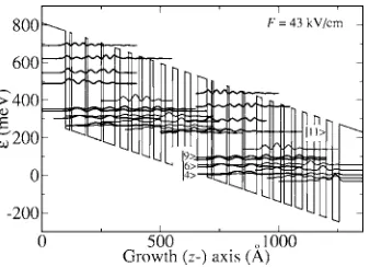
operat-ing temperature of 312 K. Figure 1 shows the moduli-squared wave functions for two periods of the device when band nonparabolicity, described via a two band Kane model, is taken into account 共see Hirayamaet al.20兲for a value of the electric field ofF= 43 kV/ cm 共the working field as esti-mated from the current-voltage characteristics of Beck
et al.兲. The structure is formed from alternate In0.52Al0.48As barriers and In0.53Ga0.47As wells that make up four regions, the active region followed by an injector region 共which
to-gether are taken to form one period of the device兲, itself
followed by another active and injector region. The laser transition takes place between the active region levels
la-a兲Electronic mail: [email protected] FIG. 1. The QC structure of Beckmoduli-squared wave functions for an applied electric fieldet al. showing two periods and theF= 43 kV/ cm.
[image:2.612.354.523.584.706.2]beled 兩11典 and兩9典 in the figure, with the levels 兩6典 and兩4典 providing rapid depopulation from the lower laser level,兩9典,
via electron-longitudinal-optical 共e-LO兲 phonon scattering
between the levels 兩9典→兩6典 and 兩6典→兩4典 共the labeling of
levels is based on the full set of solutions obtained, and the levels兩11典,兩9典,兩6典, and兩4典 correspond to the levels兩4典,兩3典, 兩2典, and 兩1典 discussed by Beck et al.兲. This mechanism is efficient because the energy separation between these levels is close to the 34 meV LO phonon energy for the In0.53Ga0.47As well material.21
These electrons are then reinjected into the adjacent re-gion, via the coupling provided by the presence of injector region miniband states, where a further laser transition takes place. Thus, the significance of the QC structure is that since layers are arranged periodically, the active region level of one period is connected to the upper laser level of the next period.
The quaternary In1−x−yAlxGayAs has become an impor-tant material for intersubband lasers because of its large con-duction band 共CB兲 offset. In particular, the specific alloy concentrations In0.52Al0.48As and In0.53Ga0.47As are of impor-tance because they are lattice matched to the readily avail-able substrates and therefore introduce no strain.22
In this report we discuss the results of our simulations for a range of lattice temperatures and doping densities, solv-ing for the scattersolv-ing rates in a self-consistent manner,
in-cluding both e-LO and electron-electron 共e-e兲 scattering
processes23–26as well as for the temperature of the nonequi-librium electron distribution.23,27This gives insight into the internal physics of the devices: An improved understanding may influence future designs.
II. MODELING
Carrier transport within the quantum cascade structure is described within a tight-binding-like picture, where any state in the long cascade is associated with one of its periods. Because of the quasiperiodicity of the structure, if共z兲is a
solution of the Schrödinger equation with energy , then
共z−D兲 is a solution with energy −⌬V, where D is the periodicity of the structure and ⌬V is the potential energy drop across one period. This allows all the states in a cascade to be constructed as replicas, shifted in space and energy, of the set of initial states. Among the states actually calculated in a structure with a finite set of periods, those that are mostly localized near the middle of the structure are the most representative of states in an infinite cascade structure, be-cause they are sufficiently remote from the boundaries and are used in the replication process.28,29
Heterostructures consist of alternate layers of dissimilar material so that the mass of the carrier is different in these layers, and to solve the Schrödinger equation we adopt the
envelope function approximation:24
再
−ប 22
d
dz
冋
1
m*共z兲 d
dz
册
+V共z兲冎
n共z兲=nn共z兲, 共1兲where the integernlabels the subbands andV共z兲is the band discontinuity at the well/barrier interface. A uniform electric
fieldF along the growth direction zmay be allowed for by
replacing the potential V共z兲 in Eq.共1兲by V共z兲+qFz, where for an electronq= −eandeis the magnitude of the charge on the electron.
III. SELF-CONSISTENT APPROACH
We start from the expression for the rate of increase of the population of theith level,
dni
dt = +
兺
f⫽infwfi−兺
f⫽iniwif, 共2兲wherei,f run over all states and over all periods andwfiis
the rate at which particles make the transition f→i which
increase the population of leveliand is identified with 1 /fi, where fi is the carrier scattering time, and similarly wif is
the rate at which particles make the transition i→f which
depopulate the leveli and is identified with 1 /if.
The major inelastic scattering mechanism in InGaAs/ InAlAs systems is via the electron-longitudinal-optical pho-non interaction, and in the calculation of the scattering rates, the processes of emission and absorption of these polar op-tical phonons were taken into account, assuming bulklike phonon modes.
Carrier-carrier scattering 共the Auger interaction兲is also an important mechanism in QCLs, particularly in those de-vices with closely spaced subbands, and we include this mechanism in determining the scattering rates.30
In principle the summation in Eq.共2兲 is taken over all possible statesffrom all the regions that make up the device. In practice this would be computationally prohibitive and the summation is taken only over two periods, together with suitable assumptions regarding the subband populations and the transition rates due to the quasiperiodicity of the structure.23,29,31
Assuming that all the levels are in the steady state, we havedni/dt= 0 giving
兺
f⫽infwfi−
兺
f⫽iniwif= 0, 共3兲
and then we can, in principle, solve forniwhen we make use of the constraint兺ini=N, whereNis the total carrier density. Note that the scattering rates also depend on the population of the levels ni,
26
so that Eq. 共3兲 is a nonlinear problem
which suggests a solution using an iterative scheme that is run until self-consistency is achieved.23
We refine the model by taking into account the subband exchange energy, as well as particles, in all scattering pro-cesses共elastic or inelastic兲. The effect of this is to introduce a carrier temperatureTethat differs from the lattice tempera-tureTl. Recent experimental and theoretical works
27,32 justify the use of a single共average兲electron temperature as a good approximation in midinfrared QCLs. The final form of the single temperature balance equation reads29
⌬=
兺
em,abs,ee兺
i,fnfwfi共f−i+␦E兲= 0, 共4兲
wheref−iis the subband energy separation and the change in energy ␦E is equal to −ELO for phonon emission 共em兲,
+ELO for phonon absorption 共abs兲, and zero for electron-electron共ee兲scattering.
Equations共3兲 and共4兲constitute the “self-consistent en-ergy balance” model, and to solve for the subband densities
niand the average electron temperature Te we use an itera-tive procedure.27,33
IV. RESULTS AND DISCUSSION
We considered several doping densities in the range 1.0⫻1017艋N
d艋2.5⫻1017 cm−3 关corresponding to sheet
densities 共10.3– 25.75兲⫻1010cm−2, respectively兴and lattice temperaturesTl= 77 and 300 K, with a range of applied elec-tric fields 5 kV/ cm艋F艋46.5 kV/ cm. We note that the re-sults reported by Becket al.correspond to a doping density
of 2⫻1017 cm−3 共giving a sheet density of 20.6
⫻1010cm−2兲, temperatures around 300 K, and applied elec-tric fields around the estimated working field of 43 kV/ cm. Often quoted are the single particle estimates for the scattering rates. These are determined by estimating the populations for the levels and then solving for the scattering rates for these populations. Table I shows our results for the single particle estimates for the emission and absorption scattering times determined from a simplified Beck structure involving only the four quantum-well active region. In this approach we solved Eq. 共1兲 for the simplified structure and make simple estimates for the subband populations of the relevant levels. Our results are in reasonable agreement with the commonly accepted values, especially in the identifica-tion of the upper and lower laser levels, for example, see Ref. 9, who quote for the emission scattering times, 11,9共e兲
= 1.88 ps, 11,6共e兲= 1.92 ps, 11,4共e兲= 2.51 ps, 9,6共e兲= 0.73 ps,
and9,4共e兲= 0.23 ps.
[image:4.612.354.521.46.173.2]Also shown in Table I are the values obtained from our calculations with self-consistently determined populations 共based upon a total sheet density of 20.6⫻1010cm−2 and a lattice temperature of 300 K兲. Inspection of Table I shows noticeable disagreement between the single particle esti-mates and the results of our self-consistent calculations. This is because the lifetimes are strong functions of the carrier densities.
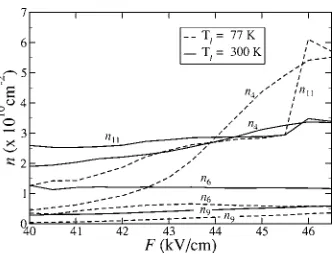
Figure 2 shows the populations for the subbands of in-terest, i.e.,兩11典,兩9典,兩6典, and兩4典, for the range of electric fields
40.0艋F艋46.5 kV/ cm and for a doping density of Nd= 2
⫻1017cm−3; the results for the other doping densities inves-tigated show similar trends.
As expected, the population of the lower laser level,兩9典, is small which is reasonable because of the fast depopulation of that level. We also note that the population of level兩6典is comparable to that of level 兩9典, but that the population of level兩4典is approximately five times larger than these and of comparable magnitude with the population of the upper laser level. Also noteworthy is that the population of level 兩4典is larger than the upper laser level for a small range of applied fields.
We now determine the current densityJby considering
the rate of flow of electrons across some reference plane, for example, the plane separating two periods. It is straightfor-ward to derive
J=q
冉
兺
i=2nd periodf=1st period
兺
niwif
−
兺
i=1st periodf=2nd period
兺
niwif
冊
, 共5兲whereqis the magnitude of the electron charge andwifis the scattering rate for the transitioni→f, so that the first double
sum in Eq. 共5兲 determines the contribution to the current
density from the second to the first period while the second double sum is the contribution from the first to the second period, i.e., back-scattering. Our results for the current den-sity are shown in Fig. 3.
Figure 3 shows the results for the current density profile for a lattice temperature of 300 K, with the result for 77 K shown as an inset. From these results we note the abrupt TABLE I. Single particle estimates compared with self-consistent scattering
times for e-LO scattering.
Single particle estimates Self-consistent results
Emission Absorption Emission Absorption
11,9共ps兲 1.20 6.84 7.06 39.08
11,6共ps兲 4.11 18.85 3.75 18.95
11,4共ps兲 4.10 17.93 6.24 30.12
9,6共ps兲 2.23 11.45 1.12 7.55
[image:4.612.50.297.72.181.2]9,4共ps兲 2.51 11.60 2.23 12.12
[image:4.612.329.459.402.455.2]FIG. 2. Variation of the subband populations with applied electric field for a doping densityNd= 2⫻1017cm−3. Note兩11典is the upper laser level,兩9典the lower laser level, and兩6典and兩4典are the relevant active region levels nec-essary for operation共see the discussion in Ref. 9兲.
[image:4.612.352.521.600.721.2]drop in the current density for applied electric fields around 25 kV/ cm, followed by a general increase for electric fields above this. Notice the evidence of “negative differential re-sistance” 共NDR兲 present for all doping densities, but more
pronounced for the larger densities, for F⬇43 kV/ cm for
300 K, but difficult to discern for 77 K.34
We also note the presence of NDR at the smaller applied fields around 30– 35 kV/ cm, again with less pronounced be-havior at the smaller lattice temperatures. This bebe-havior is related to the lining up of the upper laser level with injector levels in the next period and that it occurs for a variety of fields should come as no surprise.
The figure also shows an increase of current with doping density, partially reflecting that larger doping densities means more carriers, hence improving the dynamic working range of the QCL.
From the figure, assuming room-temperature operation
of 300 K, a doping density of Nd= 2⫻1017 cm−3, and a
working field of approximately 43 kV/ cm, we note our cal-culations to give current saturation at approximately
10 kA/ cm2 compared to 5 kA/ cm2in experiment.9
Referring back to Fig. 2, we note the rapid variation in the population of the upper laser level, n11, around the ap-plied electric fields F= 45.5– 46.0 kV/ cm 共with the larger variation at the lower lattice temperature兲. This variation takes place at around those fields where we have noted the appearance of NDR. This may be expected since from Eq. 共5兲, the current density involves the populations of all the levels关see Eq.共5兲兴and will be dominated byn11. To explain fully we would have to consider also the variation of all the levels as well as the scattering ratesi,f.
The gainGmis given as
35
Gm=⌫ 4e2具z
i,f典2共ni−nf兲
⑀0nLp2␥ , 共6兲
where is the laser emission wavelength, 2␥ is the
experi-mental full width at half maximum 共FWHM兲 of the
elec-troluminescence spectrum below threshold, n is the mode
refractive index,0is the permittivity of free space,Lpis the length of one period of the semiconductor structure共injector and active region兲,⌫is the overlap factor between the optical mode and the core active region,具zi,f典is the radiative transi-tion matrix element between the statesiandf, andniandnf are the populations of the subbandsiandf, respectively. The
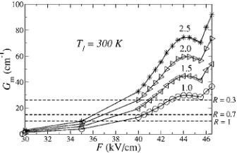
variation of the gain for the transition 11→9 with applied
[image:5.612.353.521.49.158.2]electric field for the temperature Tl= 300 K is depicted in Fig. 4. The results for the lattice temperature Tl= 77 K are broadly of similar shape.
The sharp variation of the gain profile around an applied
field of F= 45.5 kV/ cm can be explained with reference to
Eq. 共6兲 and to Fig. 2, where we have previously noted the
rapid change in n11 around this value of applied field. To
account fully for the behavior of the gain profile with applied field, we would need to examine the variation of the radiative transition matrix element.
Also shown in the figure is the threshold gaingthgiven in terms of the waveguide and mirror losses as
gth=␣+ 1 2Lln
冉
1
R1R2
冊
, 共7兲
where␣is the waveguide loss共measured by Becket al.9as 10 cm−1兲, L is the length of the cavity, and R1 and R2 are reflectivities of the mirrors taken equal to R, for values 1.0 共corresponding to perfect mirrors兲, 0.7共the value quoted by Becket al.兲, and 0.3共arbitrarily chosen for comparison兲. We notice a significant variation with doping density.
Of particular interest is the injection efficiency given as the ratio of the current to a particular active region level from the injector levels to the total current. This variation of
with applied field is shown in Fig. 5, where we show
results for injection into the upper laser level,11, and also leakage from the lower laser level, 9, for the lattice tem-peratures Tl= 77 and 300 K and for a doping density ofNd = 2⫻1017cm−3. It was noticed that the variation with doping density was marginal for a lattice temperature of 300 K and only slightly more significant for 77 K. We note that 11is
approximately 55% for the estimated working field of F
= 43 kV/ cm and decreases to approximately 45% for the
field F= 46 kV/ cm. The result for 9 shows a gradual
in-crease with field.
We discuss the injection efficiency for the upper laser level,11, in particular, noting the low value compared with the hoped-for value of unity. This can be explained by noting that injection into other levels is significant. In particular, we find that there is appreciable leakage directly to the active region levels 兩4典,兩6典,兩8典,兩9典, and兩12典. For example, the in-jection directly to level 兩12典 is appreciable at nearly 11%. FIG. 4. The variation of the gain profile for the transition 11→9 with
doping density. The doping densities are marked in the figure in units of 1017cm−3.
FIG. 5. Variation of the efficiencyfor the upper and lower laser levels with applied electric field and with temperature共䊊Tl= 77 K,쐓Tl= 300 K兲 for a doping densityNd= 2⫻1017cm−3.
[image:5.612.354.521.594.720.2]Referring to Fig. 1, we can explain this by noting that the injector levels 兩20典 and 兩23典 have energies larger than the active region levels 兩11典 and 兩12典, so that we might expect that transitions to these action region levels will be appre-ciable, particularly at higher temperatures. This is in contrast to, for example, the active region level兩13典, for which only the injector level兩23典has a larger energy, inhibiting the tran-sition兩20典→兩13典.
Of further interest is the behavior of the injection
effi-ciency around F= 45.5 kV/ cm, where we observe a rapid
increase in11. This occurs around the region of NDR共see Fig. 3兲 and is presumably related to this 共the efficiency in-volves the ratio of two currents and so is not so easy to describe兲. The behavior aroundF= 40.5 kV/ cm is more dif-ficult to explain since it would involve consideration of both the current into the upper laser level and the total current.
We now discuss our results for the electron temperature of the nonequilibrium electron distribution. Physically, it is argued that at large injected current densities, the power given to the excited electron system exceeds the rate at which the electrons relax and a nonequilibrium electron en-semble with an energy higher than the thermal reservoir is created. This continues until a steady-state is attained and the electron temperature reaches a steady value, see Ref. 33. Our results are presented in Fig. 6, where we follow Harrison
et al.,27 and consider the variation of the electron tempera-tureTewith the current densityJ, also considering its depen-dence with the doping densityNdand the lattice temperature
Tl.
Figure 6 gives our results for the variation of electron temperature with current density for the four doping densi-ties being considered for a lattice temperature of 300 K, while the inset shows the results for a lattice temperature of 77 K.
Following Ref. 27 we consider the possibility of a linear
relationship between Te andJ and define the coupling
con-stant␣e-lby the equation
Te=Tl+␣e-lJ. 共8兲
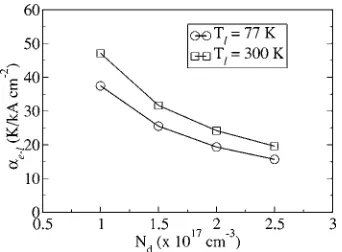
The results for ␣e-l, defined by Eq. 共8兲, and its depen-dence on the doping density and lattice temperature are shown in Fig. 7.
From this figure we note the decrease of␣e-lwith doping density, implying that as we increase the doping density the
smaller we expect the electron temperature for a given cur-rent density. We also note that as the lattice temperature de-creases then the smaller␣e-lbecomes, and so the smaller the differences we expect between lattice and electron tempera-tures to be. This is in agreement with the experimental re-sults of Troccoliet al.32
In these figures we also show the best fit lines to the data. We note that the linearity seems better for smaller lat-tice temperatures共agreeing with the comments of Ref. 27兲. Also we estimate ␣e-l⬇20– 50 K cm2/ kA for the range of doping densities considered, larger than the values quoted for the GaAs/ AlGaAs devices discussed in Ref. 27 and
compa-rable with those reported by Kohler et al.12 This may be
indicative of the important role of electron-electron scatter-ing in this device or of the influence of the material system onTe, in particular, the barrier material.
As can be determined from Fig. 7, the product␣e-lNdis almost constant for both curves, suggesting an inverse rela-tionship between␣e-landNd. We have
␣e-lNd⬇ 共38.5 ± 0.7兲⫻1017K/kA cm 共Tl= 77 K兲
⬇ 共48.0 ± 2兲⫻1017K/kA cm 共Tl= 300 K兲.
V. CONCLUSIONS
We have presented a detailed study of the impact of injector doping densities on the performance of InGaAs/ InAlAs QCLs, our simulations including a self-consistent treatment of the subband population rate equations and ac-counting for all electron-longitudinal-optical phonon and electron-electron scattering rates. We found that the emission and absorption lifetimes deduced from our full self-consistent model differed from single particle estimates. The single particle estimates are often quoted, thus emphasizing the need for detailed modeling to extract the physics of these devices accurately.
We also included in our analysis the temperature of the nonequilibrium electron distribution and found that this dif-fered significantly from the lattice temperature. We also noted that this temperature increased with the applied elec-tric field and the current density, with coupling constants somewhat larger than in analogous GaAs based midinfrared QCLs.
[image:6.612.352.523.48.174.2]The rather low injection efficiency to the upper lower laser level was noted and explained by noting the importance FIG. 6. The variation of the calculated electron temperatureTewith current
densityJand its dependence on doping densityNdand lattice temperature
Tl. The dotted lines show the best fit approximation to the data and the doping densities are marked in the figure in units of 1017cm−3.
[image:6.612.89.256.50.166.2]of the coupling of the injector region levels to the other active region levels and the relative positions of the injector and active region energies.
Finally, our estimates for the coupling constant␣e-l re-lating the electron temperature Te to the current density J
gave values of approximately 20– 50 K cm2/ kA for the
range of doping densities considered, somewhat larger than the values quoted for the GaAs/ AlGaAs devices discussed in
Ref. 27 and comparable with those reported by Kohler et
al.12This may be indicative of the important role of electron-electron scattering in this device or of the influence of the material system onTe, in particular, the barrier material.
1
J. Faist, F. Capasso, D. L. Sivco, C. Sirtori, A. L. Hutchinson, and A. Y. Cho, Science 264, 553共1994兲.
2
F. Capasso, C. Gmachl, D. L. Sivco, and A. Y. Cho, Phys. Today 55共5兲34 共2002兲.
3
C. Sirtori, Nature共London兲 417, 132共2000兲.
4
R. F. Kazarinov and R. A. Suris, Sov. Phys. Semicond. 5, 707共1971兲.
5
R. F. Kazarinov and R. A. Suris, Sov. Phys. Semicond. 6, 120共1972兲.
6
C. Gmachl, A. Trediccuci, D. L. Sivco, A. L. Hutchinson, F. Capasso, and A. Y. Cho, Science 286, 749共1999兲.
7
C. Gmachl, D. L. Sivco, J. N. Baillargeon, A. L. Hutchinson, F. Capasso, and A. Y. Cho, Appl. Phys. Lett. 79, 572共2001兲.
8
C. Gmachl, D. L. Sivco, R. Colombelli, F. Capasso, and A. Y. Cho, Nature 共London兲 415, 883共2002兲.
9
M. Beck, D. Hofstetter, T. Aellen, J. Faist, U. Oesterle, M. Ilegems, E. Gini, and H. Melchior, Science 295, 301共2002兲.
10
A. Evans, J. S. Yu, J. David, L. Doris, K. Mi, S. Slivken, and M. Razeghi, Appl. Phys. Lett. 84, 314共2004兲.
11
A. Evans, J. S. Yu, S. Slivken, and M. Razeghi, Appl. Phys. Lett.85, 2166 共2004兲.
12
R. Kohleret al., Nature共London兲 417, 156共2002兲.
13
J.-Y. Bengloan, A. De Rossi, V. Ortiz, X. Marcadet, M. Calligaro, I. Mau-rin, and C. Sirtori, Appl. Phys. Lett. 84, 2019共2004兲.
14
C. Gmachl, A. Belyanin, D. L. Sivco, M. L. Peabody, N. Owschimikow,
A. M. Sergent, F. Capasso, and A. Y. Cho, IEEE J. Quantum Electron.39, 1345共2003兲.
15
T. S. Mosely, A. Belyanin, C. Gmachl, D. L. Sivco, M. L. Peabody, and A. Y. Cho, Opt. Express 12, 2972共2004兲.
16
M. Troccoli, A. Belyanin, F. Capasso, E. Cubukcu, D. L. Sivco, and A. Y. Cho, Nature共London兲 433, 845共2005兲.
17
M. Giehler, R. Hey, H. Kostial, S. Cronenberg, T. Ohtsuka, L. Schrottke, and H. T. Grahn, Appl. Phys. Lett. 82, 671共2003兲.
18
S.-C. Lee, M. Giehler, R. Hey, T. Ohtsuka, A. Wacker, and H. T. Grahn, Semicond. Sci. Technol. 19, S45共2004兲.
19
M. Giehler, H. Kostial, R. Hey, and H. T. Grahn, J. Appl. Phys. 96, 4755 共2004兲.
20
Y. Hirayama, J. H. Smet, L. H. Peng, C. G. Fonstad, and E. P. Ippen, Jpn. J. Appl. Phys., Part 1 33, 89共1994兲.
21
Semiconductors: Basic Data, 2nd ed., edited by O. Madelung共Springer, Berlin, 1996兲.
22
J. M. Cole, L. G. Earwaker, A. G. Cullis, N. G. Chew, and S. J. Bass, J. Appl. Phys. 60, 2639共1986兲.
23
D. Indjin, P. Harrison, R. W. Kelsall, and Z. Ikonić, J. Appl. Phys. 91, 9019共2002兲.
24
G. A. Bastard,Wave Mechanics Applied to Semiconductor Heterostruc-tures共Les Editions de Physique, Paris, 1988兲.
25
J. H. Smet, C. G. Fonstad, and Q. Hu, J. Appl. Phys. 79, 9305共1996兲.
26
K. Donovan, P. Harrison, R. W. Kelsall, and P. Kinsler,Proceedings of Sixth IEEE International Conference on Terahertz Electronics, Leeds, UK, 3–4 September 1998,共IEEE, New York, 1998兲, pp. 223–226.
27
P. Harrison, D. Indjin, and R. W. Kelsall, J. Appl. Phys. 92, 6921共2002兲.
28
Z. Ikonić, R. W. Kelsall, and P. Harrison, Phys. Rev. B 69, 235308共2004兲.
29
Z. Ikonić, R. W. Kelsall, and P. Harrison, J. Appl. Phys.96, 6803共2004兲.
30
G. Scamarcio, F. Capasso, C. Sirtori, J. Faist, A. L. Hutchinson, D. L. Sivco, and A. Y. Cho, Science 276, 773共1997兲.
31
R. Bateset al., Appl. Phys. Lett. 83, 4092共2003兲.
32
M. Troccoli, G. Scamarcio, V. Spagnolo, A. Trediccuci, C. Gmachl, F. Capasso, D. L. Sivco, and M. Striccoli, Appl. Phys. Lett.77, 1088共2000兲.
33
P. Harrisonet al., Phys. Status Solidi A 202, 980共2005兲.
34
M. Giovannini, T. Aellen, T. Gresch, R. Maulini, J.-M. Bulliard, L. Sirigu, N. Hoyler, and J. Faist, 13th International Conference on Molecular Beam Epitaxy共MBE 2004兲, Edinburgh, Scotland, UK, 22–24 August 2004 共un-published兲.
35
C. Sirtori, J. Faist, F. Capasso, D. L. Sivco, A. L. Hutchinson, S. N. G. Chu, and A. Y. Cho, Appl. Phys. Lett. 68, 1745共1996兲.