Department of Engineering
PhD Thesis
Selective ablation of thin films with ultra short pulses
Thesis submitted in accrodance with the requirements of the University of Liverpool for the
degree of Doctor in Philosophy
Paul Fitzsimons
October 2012
Laser Group
Department of Engineering
University of Liverpool
Declaration
I declare that of all the work contained herein are the results of my investigations and collaborations with partner organisations.
Signed:
Paul Fitzsimons
Abstract
The micro processing of materials using ultra short pulse (USP) lasers with durations
in the low picosecond (ps) and femtosecond (fs) range allows for the possibility of precision
material removal on both nanometre and micron scales. Precision material removal can be
achieved due to the near diffraction limited focus spot size and ultra-short pulse durations,
which provide extremely high peak intensities with minimal thermal impact on the
surrounding area.
The work presented in this thesis is primarily concerned with the selective ablation of
thin films deposited on various surfaces, using lasers with picosecond temporal pulse
lengths at 1064 nm. As a result, damage to the substrate is negated through exploitation of
the difference in linear absorption coefficients between the thin film and substrate.
To elucidate the mechanism of selective processing with USP lasers; absorption,
single and multi-pulse ablation effects were investigated in both fixed and variable beam
positions. A sample of white float glass vacuum coated with indium tin oxide (ITO) was
chosen as the material for this study. Experimental results demonstrate that linear
absorption (α (λ)) of the ITO and substrate plays a key role in achieving selective thin film
ablation. As a direct consequence of the difference in absorption coefficients at 1064 nm,
the single ( ) and multi ( ) pulse ablation thresholds of both materials are altered during the high peak intensity exposure. Selective processing was achieved by exploiting the
difference between the ablation thresholds of ITO and glass. When irradiated with multiple
pulses the ablation threshold of the substrate was observed to decrease with increasing
pulse number. This change in threshold fundamentally limits the selective processing
window; therefore incubation (S) effects must be considered when determining the viability
of selective processing. For the purpose of practical applications, a series of case studies
are also presented which attempt to utilise selective materials processing. These
investigations were split into industrial and conservation. Industrial case studies focused on
successfully micro processing a small thin film ITO circuit using a Spatial Light Modulator
and a new low cost solar cell (F doped SnO2); whilst in conservation, the restoration of a pair of Royal gloves and the removal of unwanted bronze gilding is presented. The application of
USP lasers in conservation represents a relatively new field of study where little previous
research has been carried out. These case studies not only showcase the wide range of
USP applications in which selective processing can be applied but also highlight the
Acknowledgements
Firstly, I would like to thank my supervisors Professor Ken Watkins and Dr Geoff
Dearden for their help and support throughout my PhD. In addition, special thanks go to Dr
Walter Perrie for providing his guidance and support during my research and in the
preparation of this document.
I would also like to thank the other members of the laser group Olivier Allegre, Stuart
Edwardson, Eammon Fearon, Doug Eckford, Leigh Mellor, Joe Croft, Shuo “Spencer”
Shang, Zheng Kuang, Dan Welburn, Dun Liu and Jian Cheng for the fun, football and
occasional drinks. Thanks also to Andy Snaylam and Dave Atkinson for help with every
crazy idea or question I had. Special thanks go to Denise Bain for all her help, advice and
generally taking care of me for the last four years.
I would like to thank Juan Jacobo Angulo, Nick Underwood, David Vallespin,
Elizabeth Christie, Marina Carrion, Savio Varghese, Cathy Johnson, Samuel Bautista Lazo,
Giorgio Zografakis, Simao Marques, Marco Prandina and Yazdi Harmin for their friendship,
the brilliant nights out and the random conversations at lunch.
I would like to reserve a special mention for Jonathan Griffiths who I have undertaken
all my studies with during my time at Liverpool University; I count myself lucky to have had
such a great colleague and gained an even better friend.
To Laura Clews there is no way for me to express how grateful and lucky I am to
have had your love and support during the last four years; without you I would not be writing
these acknowledgements. I love you.
Finally, I would like to thank my family and friends for their support. I would
especially like to thank my Mum (Juanita Fitzsimons), Dad (Francis Fitzsimons), Aunty
Table of contents
List of Figures ... X List of Tables ... XXI List of Symbols ... XXIII
1 Introduction ... 1
1.1 Motivation and problem analysis ... 1
1.2 Primary objectives... 3
1.3 Thesis Roadmap ... 4
1.4 Thesis structure ... 4
1.5 Summary ... 5
2 Literature review ... 6
2.1 Laser fundamentals ... 6
2.1.1 Origin ... 6
2.2 Pulsed laser outputs ... 8
2.2.1 Q-switching ... 8
2.2.2 Mode-locking ... 10
2.2.3 Active mode-locking ... 10
2.2.4 Passive mode-locking ... 13
2.2.5 Chirped pulse amplification (CPA) ... 15
2.3 Characteristics of laser light ... 16
2.3.1 Monochromatic... 16
2.3.2 Directionality ... 16
2.3.3 Diffraction limited spot size ... 16
2.4 Ultra-short pulses (USP) ... 16
2.4.1 Absorption processes ... 18
2.4.2 Linear absorption ... 18
2.4.3 Nonlinear absorption ... 19
2.4.4 Reflectivity ... 19
2.5 Mechanisms of ablation ... 20
2.5.1 Metals ... 20
2.5.2 Dielectrics ... 21
2.5.3 Ablation threshold ( )... 22
2.5.4 Incubation effect ... 22
2.6 Mathematical models used in USP ... 23
2.6.1 1D two temperature model for metals ... 23
2.7 Applications ... 26
2.8 Micro-processing... 26
2.8.1 Thin film processing ... 26
2.8.2 Competing micro-processing techniques ... 27
2.8.3 Removal by mechanical force ... 27
2.8.4 Removal by etching ... 27
2.8.4.1 Dry ... 28
2.8.4.2 Wet ... 28
2.8.4.3 Reactive Ion etching (RIE) ... 29
2.8.5 Removal using lithography (LIGA) ... 31
2.8.6 Direct writing applications (DW) ... 32
2.8.7 Direct applications ... 33
2.8.8 IC and PCB industry ... 33
2.8.8.1 Scribing of thin films ... 33
2.8.8.2 Bioscience, chemistry and medical applications ... 35
2.8.8.3 MEMS and MOEMS ... 35
2.9 Laser cleaning ... 37
2.9.1 Mechanisms of laser cleaning ... 37
2.9.1.1 Selective vaporisation ... 38
2.9.1.2 Spallation... 39
2.9.1.3 Shockwave ... 40
2.9.1.4 Dry and steam cleaning ... 41
2.9.1.5 USP cleaning ... 43
2.9.1.6 Applications of laser cleaning ... 43
2.10 Selective processing of materials using laser sources ... 45
3 Experimental equipment ... 46
3.1 Clarke MXR femtosecond laser ... 46
3.2 TOPAS – C ... 47
3.3 HighQ picosecond laser ... 48
3.4 Coherent Talisker picosecond laser system ... 50
3.5 Fianium FemtoPower picosecond fibre laser ... 51
3.13 Phenom Scanning Electron Microscope ... 58
3.14 Energy Dispersive X-ray analysis ... 59
3.15 Nikon Digital Microscope ... 61
3.16 Spiricon optical beam profiler ... 61
3.17 Materials and sample preparation ... 62
4 Selective laser processing ... 68
4.1 Experimental procedure ... 70
4.1.1 Samples used in investigation ... 70
4.1.2 Absorption coefficient measurements ... 70
4.1.3 Single pulse interaction ... 70
4.1.4 Multiple pulse interaction ... 70
4.1.5 Effect of laser scanning ... 72
4.2 Results and Discussion ... 73
4.2.1 Single Pulse ablation threshold ... 77
4.2.2 Focussed spot size ... 77
4.2.3 Characterisation of single pulse ablated craters ... 82
4.2.4 Multiple pulse ablation thresholds ... 85
4.2.5 Characterisation of multi-pulse ablation ... 91
4.2.6 Effect of scanning on ITO ablation ... 94
4.3 Summary ... 102
5 Applications of selective processing ... 105
5.1 Micro processing ... 105
5.2 Parallel processing of ITO functional circuits using ultra-short pulses ... 105
5.2.1 Experimental procedure ... 106
5.2.2 Results and discussion ... 110
5.2.2.1 Single beam processing ... 110
5.2.2.2 Parallel processing ... 113
5.2.3 Summary ... 115
5.3 Selective processing of PV cells... 116
5.3.1 Experimental procedure ... 117
5.3.2 Results and discussion ... 118
5.3.2.1 Single Pulse Ablation threshold ... 121
5.3.2.2 Processing of FSO layer ... 127
5.3.2.3 Measurement of absorption coefficient ... 127
5.3.3 Summary ... 130
6 Laser Restoration ... 132
6.1.2 Result and Discussion ... 136
6.1.3 Summary ... 143
6.2 Removal of unwanted bronze gilding ... 144
6.2.1 Experimental procedure ... 145
6.2.2 Results and discussion ... 148
6.2.3 Summary ... 164
7 Conclusions and future work ... 166
7.1 Selective materials processing with ultra-short pulses ... 166
7.2 Parallel processing of a small ITO circuit... 167
7.3 Fabrication of a low cost solar cell ... 168
7.4 Restoration of a Royal accessory ... 169
7.5 Removal of bronze gilding ... 169
7.6 Future work ... 170
List of Figures
Figure 1: Laser cleaning of the statue of Linnaeus, the statue is displayed at the Palm
House, Sefton Park, Liverpool. The image shows the statue before restoration (left) and
after laser treatment (right). The contaminant layer consisted mainly of sulphur deposits. ... 2
Figure 2: 3D structures fabricated using 8 ps pulses and at 532nm with irradiances of 0.7
TWcm-2 (a) and 0.35 TWcm-2 (b). (a) is a scaffold for cell cultures and (b) a micro lens array. ... 3
Figure 3: Simplified energy level diagram for obtaining stimulated emission from an Nd:YAG
crystal. The radiative transition from level 2 to 1 produces light with a wavelength of 1064
nm. ... 7
Figure 4: Oscilloscope trace showing active (top) and passive (bottom) Q-switching.
Modulation of losses inside the cavity is used to generate ns pulses ... 9
Figure 5: Schematic representation of mode-locking in a USP laser system. A modulating
device is inserted into the cavity to alter the losses. ... 11
Figure 6: A number of longitudinal modes in the laser cavity produce the resultant output
ultra-short pulse. ... 11
Figure 7: Amplitude modulating to produce ultra-short pulses (left). The image on the right
shows how modulating the pulse when slightly out of synch with modulator causes pulse
shortening to produce the ultra-short pulses ... 12
Figure 8: Example of frequency mode-locking. Modulation is achieved through modification
of the refractive index of an intra-cavity component. ... 12
Figure 9: Example of passive mode-locking. A saturable absorber placed in the cavity is
used to modulate the light. Low intensity pulses experience high losses and are reabsorbed;
whilst the high intensity pulses are allowed to pass through experiencing low losses... 13
Figure 10: Schematic representation of a typical SESAM device. ... 14
Figure 11: The process of chirped pulse amplification. The short pulse is initially stretched
before undergoing amplification. After the stretched pulse has been amplified it is
recompressed to match the input pulse. ... 15
Figure 12: Comparison between (a) continuous wave/long pulse and (b) ultra-short pulse
laser material removal . ... 17
Figure 13: Schematic image of the band structure of three major groups of materials. The
black line represents the Fermi level. ... 21
Figure 14: Flow chart showing the steps in MD simulations. ... 25
Figure 15: AFM images comparing two aluminum electrode structures (thickness ≈ 60 nm)
fabricated (a) with a dry-etch procedure and (b) with a wet-etch procedure. ... 29
Figure 17: An image showing how the RIE process can be used to fabricate cyclinder
shaped Ag/SiO2/Au multi-segment nanopatterns. (a) PS on the Ag/SiO2/Au multi-segment surface. (b) Pattern transfer using a PDMS mold above the glass transition temperature of
PS (Tg ∼ 273.15 K). (c) Patterned PS film on the Ag/SiO2/Au multi-segment surface. (d) Removal of the residual layer by a reactive ion etching (RIE) and ion-milling process. (e)
Removal of the residual PS on top of the pattern. ... Error! Bookmark not defined.
Figure 18: A 517 μm tall copper waveguide fabricated using the LIGA process. ... 31
Figure 19: Femtosecond micro-machining of aluminum under helium at 1 kHz repetition rate
and 3.3 Wcm-2 average powers (1.4 Jcm-2/ 10 mm s-1). (a) 10 mm raster with 10/15/20/50/80 over scans. (b) 240 mm wide, 25 mm deep channel on polished aluminum sample
micro-machined at 3.3 Wcm-2 average powers . ... 33 Figure 20: SEM image of engraved micro-cavities in an integrated circuit. ... 34
Figure 21: Simplified diagram of how a photovoltaic cell converts light into electricity. ... 35
Figure 22: SEM image of a laser machined MEMS structure. This coil structure was
designed to improve cooling performance]. ... 36 Figure 23: Scanning electron micrographs showing nominal 1 mm diameter diaphragms
fabricated in 4H–SiC using a femtosecond pulsed laser: (a) profile using 0.15 mJ, 12 pulses
per spot; (b) bottom of the profile shown in (a); (c) profile using 0.05 mJ, 36 pulses per spot;
(d) bottom of the profile shown in (c) . ... 36
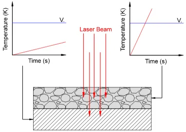
Figure 24: Principal of selective vaporisation. The graphs indicate the temperature
difference between the encrustation and substrate, which is due to differential absorption of
the incoming laser beam. The blue line (V.) represents the vaporisation point of each
material. ... 39
Figure 25: This diagram shows the mechanism of spallation. Image taken from Laser
materials processing by Steen . ... 40
Figure 26: Mechanism of shockwave laser cleaning. A focused pulsed laser is used to
breakdown the air directly above the contaminant. The expanding wave front ejects material
at the sides. ... 41
Figure 27: An image showing the mechanism involved in laser steam cleaning for the
removal of small particles from the surface of silicon wafers. ... 42
upper half. The output wavelengths available are 387nm and 775nm the frequency is 1 kHz.
... 47
Figure 30: TOPAS-C (left) is a compact system for tuning output wavelength. The image on
the right shows the TOPAS-C integrated into the Clarke MXR optical path. The laser system
is in the background whilst the TOPAS-C is on the left and the Aerotech control stage is on
the right. ... 47
Figure 31: Left: The High-Q laser with three output wavelengths of 355nm, 532nm and
1064nm. Right: control computer (top), power supply for scanning head (middle top) and
Aerotech control stage drivers (middle bottom). ... 49
Figure 32: HighQ laser control software. This interface allows the user to switch the system
on/off and to control frequency and power. ... 49
Figure 33: Talisker laser system, the laser controller (black box towards the rear of the
image) controlled the system. The laser head is the white and grey slab (in the foreground
of the image). In this section of the system the pulses are amplified and can undergo
frequency conversion to the desired output wavelength; the three outputs shown are for
1064, 532 and 355nm. ... 50
Figure 34: Fianium laser system. The system comprises a power supply (bottom right), a
controller, doped fibre oscillator and a laser head. Amplification of the pulse energy takes
place after it has left the fibre to prevent photo-darkening. ... 51
Figure 35: SLM in optical path. Beam is directed onto the LCD were user defined CGH are
displayed. The CGH is determined by the user and can be used to generated multiple
beams or as a method for pulse shaping. ... 52
Figure 36: Nutfield scanning head positioned on the HighQ system. Two galvometer mirrors
directed the beam through a 100mm flat field lens. ... 54
Figure 37: Aerotech stage (left) and driver unit (right). This stage was attached to the HighQ
lase and provided movement in 5-axis XYZUA. ... 55
Figure 38: Scanner application software (SCAPS) home screen. Laser tracks and shapes
are defined in the centre area, with variable parameters such as scan number and traverse
speed can be set in the box on the right. ... Error! Bookmark not defined.
Figure 39: Tektronic function generator; using this system it was possible to gate the laser to
emit a specific number of pulses. This enables the user to produce frequencies up to the
maximum produced by the system. ... 56
Figure 40: White light interferometry profiling system. A light source was used to illuminate
the surface of a target object; interference fringes at the focal plane are used to produce an
Figure 41: SEM area of LLEC. The SEM was a Phenom FEI scanning electron microscope.
Samples were loaded into the base unit for optical microscopy before pumping downing for
SEM. ... 58
Figure 42: Jeol SEM. In this machine samples are placed into the chamber (left, middle)
before being placed under high vacuum. Imaging and magnification is controlled using the
computer and monitor on the left of the setup. The second computer and monitor are used
to record EDX measurements. ... 59
Figure 43: Oxford Instruments Inca X-act EDX analysis machine. This system was attached
to the Jeol 6610 SEM. ... 60
Figure 44: Nikon optical microscopy system. The microscope (centre) rotates to increase
magnification; images are taken through the top down camera and transferred to the
computer terminal. ... 60
Figure 45: Spiricon profiling head. An unfocussed beam passes through a gap (left) where
it is split into two components; the majority of the beam passes through but a small portion is
diffracted onto the CCD (right). The recorded signal is then displayed on a PC. ... 61
Figure 46: Schematic of the band structure of sn-doped and undoped indium oxide []. This shows how the doping process improves conductivity by reducing the band gap allowing
more electrons to move into the conduction band. ... 63
Figure 47: Schematic of the thin film stacked photovoltaic cell manufactured in case study
two. Laser processing was used to scribe the TCO and FSO layers. ... 64
Figure 48: King Charles I gloves before laser treatment. The contamination of the white
leather is clearly visible in this image. The decorated gauntlet is also shown. These images
were taken from “Royal accessory under laser cleaning” by Abdelrazek et al []
. ... 65
Figure 49: Schematic representation of the cross section of a model sample. The structure
beneath the top layer is shown. The sample is comprised of (from top to bottom) bronze
gilding, linseed oil, white paint and a wood base. ... 67
Figure 50: Modified HighQ setup. This optical arrangement was used to determine the
absorption coefficient of the ITO thin film and glass substrate. The sample was placed after
the beam expander to ensure that the beam was collimated. A Coherent power meter with a
Fieldmaster head was used to determine the intensity of the transmitted light. ... 69
Figure 53: Schematic of the multi pulse ablation threshold test; this technique was used to
measure both ITO and glass. The number of pulses per spot (PPS) was set to 6, 10 and 25.
... 71
Figure 54: Schematic of multiple pulse ablation threshold testing. Each multiple pulse test
was grouped according to the traverse speed (X mm/s) used; within each grouping the
fluence was decreased. This was repeated for repetition rates of 5, 10 and 20 KHz. ... 72
Figure 55: Ration of transmitted light with increasing intensity. This confirms linear
absorption of the IR pulses... 76
Figure 56: Ration of transmitted light with increasing intensity. This confirms linear
absorption of the visible pulses. ... 76
Figure 57: Plot of squared crater diameters vs. pulse energy (log scale) for ITO. The
gradient of the slope was used to calculate the effective beam diameter. ... 80
Figure 58: Plot of squared crater diameters vs. pulse energy (log scale) for glass, this test
required higher pulse energies to be used due to low absorption of near IR wavelengths.
The gradient of the slope was used to calculate the effective beam diameter. ... 80
Figure 59: Plot of D2 vs. fluence for ITO (circles) and glass (squares). The regression lines remained uniform over the experimental range for both sets of data indicating the
mechanism of removal remained constant. ... 81
Figure 60: Sample of 5 craters that were used in determining the single pulse ablation
threshold of ITO. The fluences shown here are 2.12, 8.49 and 25.46 Jcm-2, for (A), (B) and (C) respectively. ... 83
Figure 61: Sample of 5 craters that were used in determining the single pulse ablation
threshold of glass. The fluences shown here are 12.73, 38.19 and 57.29 Jcm-2, for (A), (B) and (C) respectively. ... 84
Figure 62: OM images of ablated craters made using 6PPS at x20 magnification.
Measurements were made using software provided by Nikon. ... 86
Figure 63: Measurement of multi-pulse ablation threshold of ITO when irradiated with 6, 10
and 25 PPS. All processing was undertaken at 1064 nm with an oscillator repetition rate of
10 KHz. ... 89
Figure 64: Measurement of multi-pulse ablation threshold of glass when irradiated with 6, 10
and 25 PPS. All processing was undertaken at 1064 nm with an oscillator repetition rate of
10 KHz. ... 89
Figure 65: OM images of ablated craters made on ITO using 10 PPS. The fluence in these
three images decreases from 21.93 Jcm-2 (top) to 0.91 Jcm-2 (bottom). In the middle image one row of data is missing due to an error; this data was retaken later and used in the final
Figure 66: OM images of ablated craters made using 25 PPS on glass. The fluence
decreases from top to bottom; this encompasses all fluences between 16.55 and 2.55 Jcm-2. At the highest fluences (top) thermal effects around the crater edge are clearly evident.
These effects are clearly observable at the lowest fluence of 2.55 Jcm-2. ... 93 Figure 67: This SEM image (top) and EDX spectra (bottom) were recorded on an
unprocessed section of the ITO sample. The ITO coating is shown to be highly flat; the
white particulate in the middle of the lower area of the sample is a contaminant introduced
when exposed to air. ... 95
Figure 68: SEM images of ablated tracks used in pulse overlap testing. Images A, C and E
show the effect of using high pulse overlap (approx. 100 pulse per spot) with increasing
fluence; 1.43 Jcm-2 (A & B), 0.48 Jcm-2 (C & D) and 0.32 Jcm-2 (E and F). The regions enclosed by the purple line were subjected to EDX; measurements are shown in images A,
B and D. ... 96
Figure 69: Pie chart showing the relative abundance of indium after irradiation with a
constant fluence of 0.48 Jcm-2 with traverse speeds ranging between 5 – 250 mm/s. ... 100 Figure 70: Pie chart showing the relative abundance of silicon after the surface ITO layer
was irradiated with a constant fluence of 0.32 Jcm-2 at traverse speeds ranging between 5 – 250 mm/s. ... 100
Figure 71: Pie chart showing the relative abundance of indium after the surface ITO layer
was irradiated with a constant fluence of 0.48 Jcm-2 at traverse speeds ranging between 5 – 250 mm/s. ... 101
Figure 72: Pie chart showing the relative abundance of silicon after irradiation with a
constant fluence of 0.32 Jcm-2 at traverse speeds ranging between 5 – 250 mm/s. ... 101 Figure 73: The single pulse ablation threshold of ITO (red) and glass (blue) are combined
with the multi-pulse threshold of glass (green) to indicate the selective processing windows
available for single and multiple pulses. The effect of incubation on the ablation threshold of
glass is indicated. ... 104
Figure 74: Schematic representation of hatching. Overlapping in X produces a single track,
whilst overlapping in both X and Y is used to create a hatch area. ... 107
Figure 75: A schematic representation of the simple circuit fabricated on to the ITO coated
Figure 77: Image of the binary linear grating used to generate multiple beams for parallel
processing. The grating period was set to one pixel to ensure that both first order-diffracted
beams could be guided to the scanning head. ... 109
Figure 78: Spiricon image of the three beams generated using a simple binary grating. The
centre spot is the zero order beam, whilst the spots to the far left and right are the first order
diffracted beams used in circuit fabrication. ... 110
Figure 79: A white light interferometry image showing the surface of an unprocessed,
uncoated glass sample. These measurements were recorded at x50 magnification... 111
Figure 80: White light interferometry image of an ITO coated glass sample, processed using
an overlap of (a) 70%, (b) 80%, (c) 90% and (d) 95%. ... 112
Figure 81: A comparison between the surface roughness of the processed ITO coated
areas with increasing pulse overlap. The red line represents the surface roughness
recorded for uncoated glass. ... 112
Figure 82: Images of the ITO coated glass surface after parallel processing with a G1 value
of 160. The image on the left shows both fabricated circuits. The right hand image is
provided to show the size of the circuits hatched. ... 114
Figure 83: White light interferometry profile of circuits produced using non-uniform beams.
These circuits were produced using first order diffracted beams whilst the zero order beam
was blocked. This prevents overlapping of the circuits. ... 115
Figure 84: Schematic of stacked PV cell; laser processing was to be used to create the
inactive regions through selective scribing of the TCO, FSO and metal contact. This reduces
the likelihood of recombination, improving cell efficiency. ... 117
Figure 85: A schematic representation of the jig created to assist in registering the PV
samples. The blue area represents the registration point. ... 118
Figure 86: The variation of transmission ratio against impinging intensity for both the TCO
and glass sample, irradiated using the HighQ laser operating at a wavelength of 1064 nm.
... 120
Figure 87: The variation of transmission ratio against impinging intensity for both the TCO
and glass sample, irradiated using the Talisker laser operating at a wavelength of 532 nm.
... 121
Figure 88: Optical microscopy images of single pulse ablation craters produced using
fluences of (A) 31.83 Jcm-2, (B) 22.28 Jcm-2 (B) and (C) 12.73 Jcm-2 in the TCO layer. ... 122 Figure 89: Illustrating the effect of increasing fluence on the diameter squared of the ablated
craters. Extrapolation of the curve to zero indicates the single pulse ablation threshold of
Figure 90: White light interferometry image (cross section) of TCO that was processed with
a single scan of the surface (Top). The X profile (bottom) shows that a scribe of 370 nm
deep was possible with a single scan. There is no observable damage to the surrounding
material. ... 124
Figure 91: White light interferometry image of scribe made in TCO coated glass. ... 125
Figure 92: X profiles obtained from White light interferometry at different locations. In this
test the TCO surface was scanned twice to increase ablation and remove conductivity
between across the boundary. ... 126
Figure 93: Images the FSO layer deposited on to the PV cell. The photograph shows the
entire cell coated in FSO (left) and a magnification of the FSO surface (right), taken using
the Nikon microscope at x10 magnification; even at this relatively low level the high surface
roughness was apparent. ... 127
Figure 94: Left: Imaging of the scattering effect of the FSO layer produced using a HeNe
laser at 532nm. Right: SEM image of the surface roughness of the FSO layer. ... 128
Figure 95: Image of fractured sample, the red circle indicates where the failure initiated.
This damage propagated across the sample. The average power used here was 5 W with
greater than 50 surface scans being used, leading to thermal build up and subsequent
failure. ... 129
Figure 96: Optical microscopic image showing the transmission of light through FSO layer
after processing with the Clarke MXR fs laser system. Fluence of 6.11 Jcm-2 (left) and
12.22 Jcm-2 (right) were used in processing. The dark regions signify areas of no
transmittance, which are attributed to FSO remaining on the surface of the cell. ... 130
Figure 97: King Charles I gloves before laser treatment. The contamination of the white
leather is clearly visible in this image. The decorated gauntlet is also shown. ... 134
Figure 98: A photographic image showing an area of fungal growth located beneath the
gauntlet section of the glove. The red circle highlights the rust staining... 135
Figure 99: An SEM image showing the dust contaminates deposited on the dyed fabric of
the gauntlet. ... 135
Figure 100: SEM images of samples of white leather taken from the gloves, wherein the
Figure 102: Photographic images of the leather area of the King Charles I gloves during
restoration, using a fluence of 4.10 Jcm-2. Image (A) shows the glove in an early stage of the leather restoration. The colour scale is provided for comparison. ... 137
Figure 103: An image showing a section of leather restored using a fluence of 4.10 Jcm-2 when viewed at x80 magnification. No surface damage was observed, however some small
contaminant deposits remain on the surface. ... 138
Figure 104: A photographic image highlighting the complexity of the gauntlet. The red dyed
fabric, gilded fibres and gemstone eye of the animal can be observed and must be
considered during irradiation. ... 139
Figure 105: Optical microscopic images of the untreated sections of the gauntlet; (A) dyed
fabric, (B) gilt silver fabric and (C) coiled silver metal. These images were provided by
Fayoum University. ... 139
Figure 106: SEM images showing sections of the gauntlet that had been removed from the
glove. The contaminants on the surface of the (A) dyed fabric, (B) gilded fabric and (C)
metal coils are clearly visible. ... 140
Figure 107: SEM images of the (A) dyed fabric, (B) gilded fabric and (C) metal coil, after
irradiation. ... 140
Figure 108: An SEM image of a partially restored gilt silver thread. EDX spectra were
recorded for both treated (right) and untreated (left) regions, as shown above. These images
were provided by Fayoum University. ... 142
Figure 109: SEM images of the coils attached to the edge of the gauntlet. Image (A) shows
partial cleaning of the coil whilst (B) shows the coil after treatment was finished. Both
treatments used a fluence of 4.07 Jcm-2. ... 143 Figure 110: Schematic representation of the optical arrangement for the Fianium
FemtoPower 20 ps fibre laser. ... 146
Figure 111: Optical microscopic image of the top surface of a model sample before
undergoing irradiation. ... 147
Figure 112: Schematic representation of the cross section of a model sample. The structure
beneath the top layer is shown. The sample is comprised of (from top to bottom) bronze
gilding, linseed oil, white paint and a wood base. ... 147
Figure 113: High magnification (x500) SEM image of the surface of a model bronze guild
coated sample before irradiation. The black areas of the image show patches were no
bronze flakes are adhered; exposing the oil size beneath. ... 148
Figure 114: EDX spectrum of a model bronze gilded coated sample before irradiation. .... 149
times. Each column represents testing at traverse speeds of (A) 5000, (B) 500 and (C) 250
mm/s. In each test grouping the number of scans was increased from one to thirty (top to
bottom)... 150
Figure 116: Photographic image of a model sample after irradiation using a fluence of 0.81
Jcm-2. The number of scans is increased from one to thirty (left to right). The traverse speeds used were (A) 5000, (B) 500 and (C) 250 mm/s. ... 150
Figure 117: Photographic image of the model sample irradiated using a fluence of 1.22 Jcm -2
. Each column represents testing at traverse speeds of (A) 5000, (B) 500 and (C) 250
mm/s. In each test grouping the number of scans was increased between one and thirty
from top to bottom. ... 151
Figure 118: SEM image (x50) taken after irradiation with a fluence of 0.81 Jcm-2 using a traverse speed of 5000 mm/s with the maximum 30 scans (bottom). This image was used to
obtain the EDX spectra shown (top), the accelerating voltage used was 15 keV. ... 153
Figure 119: A graph showing the variation in elemental signal recorded for a processed
bronze sample when irradiated with 0.81 Jcm-2 using a traverse speed of 5000 mm/s. ... 154 Figure 120: SEM images of areas irradiated with a fluence of 0.81 Jcm-2 using a traverse speed of 500mm/s (≈ 10 PPS); the number of scans used was varied between 1 and 30.
These images show an overview of the scanned areas (A) 1 scan, (B) 10 scans, (C) 20
scans and (D) 30 scans. ... 155
Figure 121: A graph showing the variation in elemental signal recorded for a processed
bronze sample when irradiated with 0.81 Jcm-2 using a traverse speed of 500 mm/s. ... 155 Figure 122: SEM images of areas processed using a fluence of 0.81 Jcm-2 using a traverse speed of 250 mm/s (≈ 20 PPS). The number of scans is increased between 1 and 30; here
the results of (A) 1 scan, (B) 10, (C) 20 and (D) 30 scans are shown. ... 157
Figure 123: Graph showing the variation in elemental signal obtained when irradiated with a
fluence of 0.81 Jcm-2 using a traverse speed of 250 mm/s. The dotted lines represent the boundaries of bronze/oil size (left) and titanium/wood. ... 158
Figure 124: SEM images of areas irradiated at a fluence of 1.22 Jcm-2 with a traverse speed of 5000 mm/s. This image shows the result of (A) 1 scan, (B) 10, (C) 20 and (D) 30 scans.
... 159
Figure 127: Graph showing the variation in elemental signal obtained when irradiated with a
fluence of 1.22 Jcm-2 using a traverse speed of 5000 mm/s. The dotted lines represent the boundaries of bronze/oil size. ... 161
Figure 128: SEM images of areas processed using a fluence of 1.22 Jcm-2 with a traverse speed of 250 mm/s. This image shows the result of (A) 1 scan, (B) 10, (C) 20 and (D) 30
scans. ... 161
Figure 129: Graph showing the variation in elemental signal obtained when irradiated with a
fluence of 1.22 Jcm-2 using a traverse speed of 250 mm/s. The dotted lines represent the boundaries of bronze/oil size (left) and titanium/wood (right). The dotted lines indicate the
gilding/oil size interface (left) and oil size/sealing layer interface (right). ... 162
Figure 130: Using a fluence of 1.22 Jcm-2 with a traverse speed of 500 mm/s and a maximum 20 scans, the gilded frame section was irradiated to test the use of laser treatment
on real conservation items. The bronze gilding on the surface was removed revealing the
wood base and some gold leaf, which had previously been covered hidden due to the
List of Tables
Table 1: This table shows the incident (P0) and transmitted (P1) power measurements for glass and ITO when irradiated with near IR wavelengths (1064 nm). The transmitted powers
for ITO were adjusted to account for the glass substrate. ... 73
Table 2: This table shows the incident and transmitted power measurements for glass and ITO when irradiated with a visible wavelength (532 nm). As in Table 1 ITO data was adjusted to account for the glass substrate. ... 74
Table 3: Intensity of incident and transmitted laser pulses for ITO and glass when irradiated with 1064 nm pulses. ... 74
Table 4: Intensity of incident and transmitted laser pulses for ITO and glass when irradiated with 532 nm pulses. ... 75
Table 5: Data used to calculate the effective beam diameter and single pulse ablation threshold of ITO when irradiated with 10 ps pulse at the fundamental wavelength. ... 78
Table 6: Data used to calculate the effective beam diameter and the single pulse ablation threshold of glass when irradiated with 10 ps pulse at the fundamental wavelength. ... 79
Table 7: Six pulse ablation threshold of ITO when irradiated with 1064 nm. ... 86
Table 8: ten pulse ablation threshold of ITO when irradiated with 1064 nm. ... 87
Table 9: Twenty-five pulse ablation threshold of ITO when irradiated with 1064 nm. ... 87
Table 10: Six pulse ablation threshold of uncoated glass when irradiated with 1064 nm. .... 87
Table 11: Ten pulse ablation threshold of uncoated glass when irradiated with 1064 nm. ... 88
Table 12: Twenty-five pulse ablation threshold of uncoated glass when irradiated with 1064 nm. ... 88
Table 13: Multi-pulse ablation threshold and effect of incubation on ITO. Pulse trains of 6, 10 and 25 PPS were used; the single pulse ablation threshold is provided for comparison. 90 Table 14: Multi-pulse ablation threshold and effect of incubation on ITO. Pulse trains of 6, 10 and 25 PPS were used; the single pulse ablation threshold is provided for comparison. 90 Table 15: This table shows the indium abundance recorded after irradiation with a constant fluence of 0.48 Jcm-2 at traverse speeds between 5-250 mm/s. The abundance recorded at zero is taken from an unprocessed region and used as the reference for calculating the percentage change in abundance. ... 97
Table 17: This table shows the silicon abundance recorded after irradiation with a constant
fluence of 0.48 Jcm-2 at traverse speeds between 5-250 mm/s. The reference abundance was taken from an unprocessed region and highlights the increase in silicon signal as ITO
was removed from the surface. ... 98
Table 18: This table shows the silicon abundance recorded after irradiation with a constant
fluence of 0.32 Jcm-2 at traverse speeds between 5-25 mm/s; above 25 mm/s the fluence was too low to initiate ablation. The reference abundance was taken from an unprocessed
region and highlights the increase in silicon signal as ITO was removed from the surface. . 98
Table 19: Variation of transmitted power when altering G1. Only the first orders were used
in processing, however zero order data has been included for completeness. ... 114
Table 20: Impinging and transmitted intensities recorded for 1064 nm radiation on glass and
F-SnO2. As F-SnO2 was coated on to the glass surface,the intensity values were adjusted to factor in the glass substrate. ... 119
Table 21: Impinging and transmitted intensities recorded for 532 nm radiation on glass and
F-SnO2. As F-SnO2 was coated on to the glass surface,the intensity values were adjusted to factor in the glass substrate. ... 120
List of Symbols
Symbol
Description
Units
Linewidth of laser transitions nm
Ablation threshold Jcm-2
( ) Single pulse ablation threshold Jcm-2 ( ) Ablation threshold for N pulses Jcm-2
Electron heat capacity
Minimum beam diameter m
Input beam diameter m
Average Fluence Jcm-2
Peak Fluence Jcm-2
Force on an atom N
I Average Intensity Wcm-2
Peak Intensity Wcm-2
Initial intensity Wcm-2
Electron thermal conductivity
Beam quality factor -
Pulse width s
Electron temperature K
Lattice temperature K
Thermal velocity of atom
Focal length m
Mass of an electron Kg
Mass of atom Kg
Position of atom Critical plasma density
Angle of incident rays Degrees
Focussed beam diameter μm
Laser frequency Rads-1
Permittivity of free space Fm-1
D Absorption depth m
D Diameter m
E Charge on an electron C
I Atom -
K Extinction coefficient -
N Refractive index -
N Number of pulses -
R Reflectivity (metals) -
Reflectivity p polarisation - Reflectivity s polarisation -
T Time S
Z Distance from first boundary m
1.1 Motivation and problem analysis
Thin film is a term applied to layers of materials which range from nanometres up to a
millimetre in thickness, with such a broad definition this means that the composition and
properties of these materials are wide ranging; for example thin films have been widely
adopted in microelectronics (e.g. flat screen displays) and optical coatings, such as high k
dielectrics for anti-reflection lens coatings. In contrast, thin films observed in conservation
can damage or ultimately destroy items which can be of high value but more importantly are
irreplaceable.
The uses of thin films in microelectronics are widespread and they are a key
component in many electronic devices, such as high-density circuit boards, touch screen
panels, photovoltaic cells and strain gauges.
The main manufacturing steps in micro fabrication are high temperature substrate
modification, thin film deposition, patterning and bonding; within these four basic operations
there can be several further fabrication steps. Currently, manufacturing methods for these
devices are time consuming and expensive.
The market for electronic products continues to grow; therefore to successfully
compete manufacturers need to provide the latest technology at the lowest possible cost to
the consumer. One method of achieving this is through improvement of current
manufacturing methods; this offers several advantages including: a reduction in cost,
increased process efficiency, improved throughput, less waste and potential new
functionality.
To date, the application of lasers in thin film removal has mostly been undertaken
using short pulse (≥ns) or continuous wave lasers. The main drawback of using these
systems has been high thermal input at the surface and shockwaves generated on or near
the surface resulting in thin film removal but also substrate damage.
Thin films do not always provide beneficial properties; in some instances the film
causes deterioration of the substrate. This detrimental effect is most easily observed in
conservation. Over time films form on the surface of art and heritage objects with the
composition and thickness of the film being dependent upon the environment in which the
piece is displayed. A good example is the many statues located in urban areas, the
contaminants on which consist mostly of carbon and sulphur deposits [1] produced by motorised transport; figure 1 highlights the beneficial effect of laser treatment. Before
processing the surface of the statue was covered in surface deposits (left) and after
these films can vary from reduced aesthetics to partial corrosion and ultimately destruction of
the object; therefore removal of these films is of significance in preserving art and heritage
pieces.
Traditional restoration techniques involve the use of either physical abrasives or
chemical breakdown of the layer; these methods of removal are time consuming, can be
difficult to implement and are not always effective. The application of lasers to conservation
began in the late 70s and has since become a key tool for conservators; resulting in the
publishing of several books on the subject [1, 2] and establishing the LACONA conference dedicated to the application of lasers in restoration.
Figure 1: Laser cleaning of the statue of Linnaeus, the statue is displayed at the Palm House, Sefton Park, Liverpool. The image shows the statue before restoration (left) and after laser treatment (right). The contaminant layer consisted mainly of sulphur deposits [3].
In subtractive processes, selective processing describes the removal of individual
layers from a multi-layer substrate as a consequence of the difference in absorption. Using
long pulse (LP) or continuous wave (CW) lasers, selective material removal has been
applied to both macro fabrication and laser conservation; for example the first restoration
mechanism identified was named selective removal [4]. Through selective material removal laser processing of thin films becomes much easier and quicker as the user no longer has to
consider substrate effects beyond knowing the damage threshold.
Ultra-short diode pumped solid state lasers emit pulses with durations of typically
using an ultra-short laser source it is possible to ablate most materials, including diamond [6], which due to the high peak intensities can be mediated by both linear and non-linear
absorption. All of these advantages can be attributed to ultra-short pulse (USP) laser
systems.
Due to recent advances in ultra-short laser technology the commercial application of
USP systems has increased. When combined with high accuracy CNC tables it is possible
to fabricate extremely small and complex structures on thin films. Figure 2(a) and 2(b) show
micro-components fabricated using ultra short pulse lasers. Both these figures highlight the
ability of ultra-short pulses to generate clean, precise and complex structures. Similarly, in
restoration this high precision can be utilised to only irradiate the necessary areas of an
object, preventing unwanted exposure of other parts.
Figure 2: 3D structures fabricated using 8 ps pulses and at 532nm with irradiances of 0.7 TWcm-2 (a) and 0.35 TWcm-2 (b). (a) is a scaffold for cell cultures and (b) a micro lens array [7].
1.2 Primary objectives
The aim of this thesis is to highlight the capabilities of ultra-short picosecond pulse
lasers as a disruptive technology for selective ablation of thin films; research was focused on
the factors controlling selective removal, methods of manufacturing functional devices and
the restoration of art and heritage items. The main objectives of this thesis are:
To elucidate the factors controlling selective removal of thin films using ultra short
pulses.
To demonstrate the use of selective removal in micro-processing. To demonstrate the use of selective removal in laser conservation. Identify selective operating parameters on various thin films.
This was achieved through a series of planned experiments and process optimisation
1.3 Thesis Roadmap
1.4 Thesis structure
This thesis is presented as follows:
Chapter 2 provides an introduction to relevant background information on selective processing, thin film micro-processing and laser conservation. A literature review of
ultra-short pulse laser technology and its application in micro fabrication and restoration is
included. Ultra-short pulse laser ablation mechanisms, related experiments and results are
analysed.
Chapter 3 provides a description of the experimental equipment, setup and methodology used to implement and analyse the experiments described in this thesis.
Details of the materials used in testing are also provided.
Chapter 4 presents the results obtained from an investigation into the factors governing selective processing. Using an ITO thin film adhered to a glass substrate the
Selective ablation of thin films with ultra short pulses
Factors controlling selective removal
Micro-processing
Direct Writing of
ITO Photovoltaic cell
Laser Restoration
Removal of Bronze Gilding
and the removal of unwanted bronze gilding. Through these case studies the usefulness of
selective processing techniques, advantages and limitations are identified.
Chapter 6 concludes this thesis, providing a summary of its findings and achievements. Suggestions are provided for future research directions based on the work
presented herein.
1.5 Summary
Currently, thin film devices are expensive to design and manufacture due to
economies of scale, the availability of suitable materials and technological readiness.
However, market demand for new products which utilise thin films is extremely strong (e.g.
LCD TVs and mobile phones). As such new methods of manufacturing these devices that
can reduce costs and improve throughput are highly sought after.
Similarly, in conservation practice ultra-short lasers have the potential to become an
extremely useful tool; this is due to development of new more robust systems which can
operated outside controlled laboratory conditions. The cost of these systems is reduced
making these lasers more accessible to conservators. Current non-laser restoration
techniques are labour intensive, require hazardous chemicals and are time consuming;
whilst current laser techniques have been limited in scope due to the thermal input at the
surface.
Presently, the use of selective removal using ultra-short pulse lasers has received
little attention. However, by using this technique in conjunction with precise material removal
associated with ultra-short pulse laser there are several potential benefits including: greater
efficiency, lower costs and higher throughput whilst ensuring no substrate damage occurred.
This would improve the micro fabrication process and offer conservators a new tool
2
Literature review
This chapter presents some relevant background to lasers and ultra-short pulse (USP)
laser processing. Reviews of laser technology, laser-material interaction mechanisms and
the micro-processing techniques currently available in the literature are presented. In this
thesis the author focuses on two specific areas: the micro-processing of thin films and
restoration treatments. In addition, a state of the art review is conducted on the current
applications of laser technology in both thin film processing and restoration.
2.1 Laser fundamentals
2.1.1 Origin
The physics underlying stimulated emission where first postulated by Einstein in
1917 [8] and confirmed experimentally by Ladenburg in 1928 [9]. However, it was not until May 1960 that the first laser was demonstrated by Theodore Maiman; this system used a
Ruby crystal as the gain medium and can still be operated today, 50 years after it was first
constructed [10,11].
Soon after, many different laser systems were invented. Javan et al [12], at Bell laboratories, developed the first gas laser from a mixture of helium and neon in 1961. Two
years later, in 1963, Patel [13] also from Bell laboratories invented the CO2 laser, which has become one of the most powerful and widely used industrial lasers. Today, CO2 lasers are used in welding [14], cutting [15], forming [16,17], cladding [18] and repair [19].
The application of solid-state ultra-short pulse lasers in selective materials
processing is the primary focus of this study; the development of these laser systems from
their origin is subsequently discussed.
The Ruby laser developed by Maiman [3, 4] was the first solid-state system as well as the first working laser. Solid-state lasers (SSL) utilise a gain medium such as crystals (Ruby
laser) or glasses doped with a rare earth or transition metal ions (for example Nd:YAG) [20]. A simplified energy level diagram of a Nd:YAG SSL is shown in figure 3. Initially, the gain
medium is pumped using flash lamps or diodes, the latter being the most commonly used
today, to excite electrons to a higher energy level (figure 3 (level 3)). The close proximity of
separation between the levels of 0 (figure 3 (ground state)) and 1 are also closely spaced,
resulting in a rapid relaxation to the ground state, with no output radiation.
Diode pumped solid-state lasers are often referred to as DPSS or all-solid-state
lasers. DPSS systems are generally preferred to flash pumped systems (FPSS) as they
have a longer operating life and a higher conversion efficiency, whilst consuming less power
when compared to FPSS lasers.
Figure 3: Simplified energy level diagram for obtaining stimulated emission from an Nd:YAG crystal. The radiative transition from level 2 to 1 produces light with a wavelength of 1064 nm.
Population inversion is key to producing a laser output and requires the majority of
atoms in the lasing medium to be in the metastable level. Photons are emitted when
electrons spontaneously decay (spontaneous emission) to a lower level (figure 3 (level 1))
before undergoing a further non-radiative decay back to the ground state.
If the photon released has an energy (E2 – E1) it can stimulate another atom in the metastable state to release a photon with the same phase, energy and momentum as the
original; this process is called stimulated emission [1, 2, 7]. The vast majority of these stimulated photons are lost through collisions with the sides of the lasing medium. However,
some photons will travel parallel to the optical axis of the cavity and are trapped by mirrors
positioned at either end. One mirror is a totally reflecting surface whilst the other is partially
reflecting; this allows a small proportion of the photons to pass through and out of the cavity.
Photons that do not pass through are reversed back to continue the stimulated emission
[image:30.595.136.457.205.447.2]If the lasing medium is continuously pumped eventually equilibrium is established
between the number of atoms at the metastable state and the number of emitted photons,
resulting in a continuous emission.
2.2 Pulsed laser outputs
Through modulation of the lasing cavity output, it is possible to generate “flashes” of
light; also known as an optical pulse. A pseudo method of producing a pulsed output can be
achieved via beam blocking or using a spinning prism. Pulsed laser systems have been
found to be able to generate light pulses with temporal pulse durations from micro- to femto-
seconds and more recently pulse durations of attoseconds [22] with high spatial coherence; allowing for near diffraction limit focused beam diameters (2ω0 < 30 μm). The combination of these properties allows for extremely high peak powers from commercial laser systems (P
≥ GW) and ultra-high focussed intensities (I >> 10 TWcm-2) even with modest pulse energies.
There are several different methods for generating laser pulses; the technique used
varies depending on the pulse requirements. As this study utilises ultra-short pulse lasers
the following section will focus on describing the techniques commonly used to generate
these pulses.
2.2.1 Q-switching
Maiman’s laser [3, 4] is an example of a pulsed laser. Further work by Collins et al. on Ruby lasers demonstrated pulses emitted on millisecond (ms) timescales [23]. This sparked further interest among researchers to produce more defined pulses. The first solution was
proposed in 1961 by Hellwarth et al. [24] and was later confirmed experimentally by McClung
et al. (1962) [25] with the production of low order nanosecond pulses (ns); this technique was referred to as Q-switching.
Q-switching is used to obtain high-energy short (>ns) but not ultra-short pulses.
Pulse durations between one and several hundred nanoseconds can be generated with this
method. Using a Q-switching laser it is possible to generate peak powers many times
greater than the average powers produced by continuous wave (CW) lasers. These powers
range from MW to GW. These lasers have proven to be particularly useful in several
stimulated emission. Once the gain in the cavity is saturated, the maximum pulse energy
has been reached and is emitted as an output pulse. Figure 4 shows the temporal evolution
[image:32.595.112.445.154.698.2]of gain and losses in both active and passive Q-switched lasers.
Control of the cavity losses is achieved through either passive or active Q-switching.
Active control requires the use of a modulating device, which is triggered by an external
source (outside the cavity). In contrast, the losses in passive Q-switching are self-modulated
through the use of a saturable absorber. In this technique losses are minimised when the
energy in the lasing medium reaches a sufficiently high intensity.
Q-switched lasers utilising this method of pulse generation have found widespread
use in industry and conservation. Whilst it is not possible to generate ultra-short pulses with
this technique it is currently one of the most common techniques used in commercially
available laser systems.
Laser systems that can generate optical pulses with a temporal duration ranging from
picoseconds (10-12 s) to femtoseconds (10-15 s) are classified as ultra-short pulse lasers. To generate ultra-short laser pulses, mode-locking (active or passive) combined with chirped
pulse amplification (CPA) are often employed.
2.2.2 Mode-locking
Mode-locking refers to a group of techniques developed for the generation of
ultra-short laser pulses. This method of generating ultra-ultra-short pulses (USP) was first proposed by
Lamb Jr. in 1964 [28], before being observed experimentally by Hargrove et al. [29] later that year.
Inside the laser cavity each longitudinal mode will oscillate randomly with no fixed
relationship to one another; this gives rise to the continuous output observed in CW lasers.
To generate ultra-short pulses, these modes are forced to operate with a fixed phase
relationship between one another; when operating in this manner the laser output is
drastically altered as shown below in figures 5 and 6. Such lasers are said to be
mode-locked and can be used to emit ultra-short optical pulses.
The pulse duration produced is dependent upon the number of modes oscillating
within the laser cavity; therefore lasing mediums with a large gain bandwidth are able to
generate the shortest pulses. The methods of mode locking are discussed in the following
paragraphs.
Figure 5: Schematic representation of mode-locking in a USP laser system. A modulating device is inserted into the cavity to alter the losses.
Figure 6: A number of longitudinal modes in the laser cavity produce the resultant output ultra-short pulse.
AM involves altering resonator losses within the cavity using a modulating device
such as an electro-optic or acousto-optic modulator; this acts as a ‘shutter’ allowing
synchronised ultra-short pulses to pass through whilst stopping longer pulses. Short pulses
that pass through the modulator whilst it is ‘open’ are subjected to small losses and can
complete another cavity round trip increasing the number of short pulses. Conversely,
radiation outside of this time frame is subjected to large losses.
If a pulse arrives too early the leading edge is reduced in intensity, moving the
remaining peak of the pulse to later times and closer to synchronisation with the AM device.
Intensity attenuation on each round trip causes shortening of the pulse duration until
equilibrium is reached (figure 7). Equilibrium is reached when pulse shortening is offset by
other effects such as gain narrowing; the minimum pulse duration attainable is established
when equilibrium is reached. A pulse arriving after the opening window has closed
Figure 7: Amplitude modulating to produce ultra-short pulses (left). The image on the right shows how modulating the pulse when slightly out of synch with modulator causes pulse shortening to produce the ultra-short pulses [31].
FM mode-locking (figure 8) is achieved by modulating the refractive index of the
intra-cavity component; as light passes through the device a small shift in frequency is
induced. When the round trip time is synchronised with the frequency modulator some light
is shifted to longer or shorter wavelengths; after several round trips these are removed from
the cavity as the wavelength is outside the gain bandwidth.
However, when the induced frequency shift is zero, light is allowed to pass through
and complete another cavity round trip; eventually after several round trips narrow ultra-short
[image:35.595.132.457.461.723.2]2.2.4 Passive mode-locking
Passive mode-locking was initially called Q-switched mode-locking, as it was first
demonstrated together with Q-switching by Mocker et al. (1965) [33]. Passive mode-locking has a key advantage over active mode-locking; with this technique it is possible to produce
pulses of a much shorter duration. All laser systems in this study produce ps pulses via
passive mode-locking. Generally, determining the pulse width of a passively mode-locked
laser is more difficult and must be considered on a case-by-case basis. However, the lower
limit of attainable pulse widths (Td) can still be determined using equation 1.1:
(1.1)
Where is the linewidth of the laser transition. The arrangement for passive mode-locking is the same as an active system; however in a passive system the optical element is
not actively modulated with an external driver. The transmission properties observed during
passive mode-locking are dependent upon the intensity of the incident radiation. The
temporal variation observed during passive mode-locking using a fast saturable absorber is
[image:36.595.95.509.444.664.2]shown in figure 9.
Figure 9: Example of passive mode-locking. A saturable absorber placed in the cavity is used to modulate the light. Low intensity pulses experience high losses and are reabsorbed; whilst the high intensity pulses are allowed to pass through experiencing low losses [34].
mode-time of the saturable absorber must be shorter than one cavity round trip. Slow saturable
absorbers have a recovery time near to, but still less than, the cavity round trip time.
There are several methods of creating artificial absorbers; one example of this is
Kerr lens mode-locking. In this technique an artificial saturable absorber is created by
exploiting the Kerr effect [36]; wherein a change in the refractive index of a material is observed in response to an applied electric field. Using this technique it is possible to
generate pulses of < 10 fs [37].
Fast saturable absorbers have a recovery time significantly shorter than the round
trip time, typically a few picoseconds or less [22]. When placed in a cavity the saturable absorber induces low losses for high intensity pulses and high losses for low intensity ones.
This produces a single high intensity pulse within the cavity; other lower intensity pulses are
reabsorbed.
Semiconductor saturable absorber mirrors (SESAM) are an example of a fast
saturable absorber, displaying recovery times of the order of 100 fs [23]. This extremely fast response time is a key factor in determining the final pulse duration.
A SESAM comprises a semiconductor material encased between two mirrors; a
typical SESAM is shown schematically in figure 10. The spacing of the mirrors within the
SESAM device is crucial to prevent damage to the semiconductor material, which typically
has a low saturation and damage threshold.
2.2.5 Chirped pulse amplification (CPA)
For ultra-short pulse (USP) lasers with high repetition rates, the pulse energy
produced can be of the order of nano-Joules (nJ). This is too low for materials processing to
be viable, consequently these pulses must be amplified. However, the resulting amplified
pulses pose a problem, as the peak intensity is extremely high (>TW), leading to effects
such as non-linear pulse distortion (self phase modulation and self focussing) and damage
to the gain medium or other optical components. To overcome this, chirped pulse
amplification (CPA) is utilised (figure 11). This technique was first demonstrated by Mourou
and Strickland [38] and can be used to amplify fs pulses up to petawatt peak powers (1015 W) without any of the deleterious effects mentioned.
In this technique pulses are initially passed through a dispersive element, such as a
grating pair or long fibre, which stretches the pulse temporally, reducing the peak intensity to
well below the non-linear threshold avoiding damage. The stretched pulse then passes into
the amplifier were the energy is increased to much higher levels (G ≈106), more suitable for materials processing (≈µJ). After amplification the pulse enters a dispersive compressor
(typically a grating pair) which has the opposite dispersion to the stretcher, removing the
chirp. This returns the amplified pulse to high intensities before being emitted. This method
is only applicable to extremely short pulse lengths from the low femtosecond regime to a few
picoseconds.

![Figure 4: Oscilloscope trace showing active (top) and passive (bottom) Q-switching. Modulation of losses inside the cavity is used to generate ns pulses [27]](https://thumb-us.123doks.com/thumbv2/123dok_us/8058394.225358/32.595.112.445.154.698/figure-oscilloscope-showing-active-passive-switching-modulation-generate.webp)
![Figure 7: Amplitude modulating to produce ultra-short pulses (left). The image on the right shows how modulating the pulse when slightly out of synch with modulator causes pulse shortening to produce the ultra-short pulses [31]](https://thumb-us.123doks.com/thumbv2/123dok_us/8058394.225358/35.595.132.457.461.723/figure-amplitude-modulating-produce-modulating-slightly-modulator-shortening.webp)

![Figure 20: SEM image of engraved micro-cavities in an integrated circuit [105].](https://thumb-us.123doks.com/thumbv2/123dok_us/8058394.225358/57.595.128.470.78.350/figure-sem-image-engraved-micro-cavities-integrated-circuit.webp)
![Figure 21: Simplified diagram of how a photovoltaic cell converts light into electricity [108]](https://thumb-us.123doks.com/thumbv2/123dok_us/8058394.225358/58.595.189.408.73.346/figure-simplified-diagram-photovoltaic-cell-converts-light-electricity.webp)
![Figure 22: SEM image of a laser machined MEMS structure. This coil structure was designed to improve cooling performance [112]](https://thumb-us.123doks.com/thumbv2/123dok_us/8058394.225358/59.595.168.428.432.713/figure-machined-structure-structure-designed-improve-cooling-performance.webp)
![Figure 25: This diagram shows the mechanism of spallation. Image taken from Laser materials processing by Steen [125]](https://thumb-us.123doks.com/thumbv2/123dok_us/8058394.225358/63.595.109.498.158.429/figure-diagram-mechanism-spallation-image-laser-materials-processing.webp)

