This is a repository copy of Atomic Defects in Two-Dimensioal Materials: From
Single-Atom Spectroscopy to Functionalities in Opto-/Electronics, Nanomagnetism, and Catalysis.
White Rose Research Online URL for this paper: http://eprints.whiterose.ac.uk/133763/
Version: Accepted Version
Article:
Hong, Jinhua, Jin, Chuanhong, Yuan, Jun orcid.org/0000-0001-5833-4570 et al. (1 more author) (2017) Atomic Defects in Two-Dimensioal Materials: From Single-Atom
Spectroscopy to Functionalities in Opto-/Electronics, Nanomagnetism, and Catalysis. Advanced Materials. 1606434. ISSN 0935-9648
[email protected] https://eprints.whiterose.ac.uk/
Reuse
Items deposited in White Rose Research Online are protected by copyright, with all rights reserved unless indicated otherwise. They may be downloaded and/or printed for private study, or other acts as permitted by national copyright laws. The publisher or other rights holders may allow further reproduction and re-use of the full text version. This is indicated by the licence information on the White Rose Research Online record for the item.
Takedown
If you consider content in White Rose Research Online to be in breach of UK law, please notify us by
Submitted to DOI: 10.1002/adma.((please add manuscript number))
Article type: Review
Atomic defects in two-dimensional materials: from single-atom
spectroscopy to functionalities in opto/electronics, nanomagnetism and
catalysis
Jinhua Hong1, Chuanhong Jin1, *, Jun Yuan1, 2, *, Ze Zhang1, *
Dr. Jinhua Hong, Prof. Chuanhong Jin, Prof. Jun Yuan, Prof. Ze Zhang
1State Key Laboratory of Silicon Materials, School of Materials Science and Engineering, Zhejiang
University, Hangzhou, Zhejiang 310027, P. R. China
Prof. Jun Yuan
2Department of Physics, University of York, Heslington, York, YO10 5DD, United Kingdom
Keywords: point defects, S/TEM and EELS-ELNES/EXELFS, electronic structure,
nanomagnetism, catalysis
Abstract: Two-dimensional layered graphene-like crystals including transition metal dichalcogenides (TMDs) have received extensive research interest due to their diverse
electronic, valleytronic and chemical properties, with the corresponding optoelectronics and
catalysis application being actively explored. However, the recent surge in two-dimensional
materials science is accompanied by equally great challenges such as defects engineering in
the large-scale sample synthesis. It is necessary to elucidate the effect of structural defects on
the electronic properties, in order to develop an application-specific strategy for the defect
engineering. Here in this paper, we review the two aspects of the existing knowledge of native
defects in two-dimensional crystals. One is the point defects emerging in graphene and
hexagonal boron nitride as probed by atomically resolved electron microscopy and their local
electronic properties as measured by single-atom electron energy-loss spectroscopy. The
other will focus on the point defects in TMDs and their influence on the electronic structure,
photoluminescence and electric transport properties. Our review of atomic defects in
two-dimensional materials will offer a clear picture of the defect physics involved to demonstrate
the local modulation of the electronic properties and possibly benefit in potential applications
in magnetism and catalysis.
Published in Advanced Materials Vol.29, issue14, 1606434
1. Introduction
The discovery of graphene[1-10] and subsequent development of other graphene-like layered
materials[11-17] have defined the history of two-dimensional materials research, which sparks
considerably the exploration of low-dimensional condensed matter physics[2, 6, 8, 9, 16] and
enrich the two-dimensional crystal family[18]. In the past decade, extensive research efforts
have also been made in the exploitation of electric, optical and optoelectronic properties of 2D
materials.
1.1 The rise of the 2D families
Modern electronics is fast developing in a trend that devices are becoming smaller, faster
and cheaper[19], as exemplified by the Moore’s Law. For example, TSMC and Intel are now
already approaching the scaling extreme of 10nm and 7nm, respectively, below which
quantum tunnelling or short channel effect[20] will occur. Many 2D materials have been
considered as promising candidate[21] to break out the 5-nm theoretical scaling limit[22] of
silicon transistors according to the Moore’s Law. Very recently, Desai et al.[23] successfully
demonstrated MoS2-based transistors with 1-nm gate length using carbon nanotube as the gate
electrode. The excellent switching performance[23] with nearly ideal sub-threshold swing and
a high on/off ratio provides an exciting paradigm for 2D materials to open up a new era of
highly-integrated 2D electronics alternative to the silicon-based microelectronics. The
endeavor in discovering and engineering non-silicon 2D ultrathin channel materials[21] in
transistor applications has never stopped, which now is marked by the coming of the era of
2D crystals and post-silicon electronics. As a large group, two-dimensional (2D) layered
materials possess several distinct structural properties and diverse physical functionalities,
ranging from superconductor, (semi)metal, semiconductor to insulator. As the corresponding
typical member of 2D family, graphene, boron nitride (BN) and transition metal
dichalcogenides (TMDs)[24] hold different promising potentials not only in electric,
optoelectronic applications, but also in magnetic and catalytic chemistry. The former
functionalities are closely associated with the intrinsic electronic structure, while the latter
usually results from localized defect states. The band structure engineering linked through
understanding of the structure-property correlation is a key topic of the nanophysics of 2D
materials.
1.2 Why point defects?
Band engineering resides at the heart of modern microelectronics. The route to tailoring
the electronic structure can be traced back to the modulation of the atomic structure by defects,
Submitted to
optoelectronic devices[25] and GaN-based light emitting diodes[26, 27] constitute the foundation
of vast majority of modern electronics industry, which can be ascribed to great success of
modern band engineering technology. Although the 2D material systems could be the hope of
future electronics, their band modulation/engineering has not been extensively explored as the
techniques responsible for the mature silicon semiconductor systems. Thus there is still a huge
gap between the advance in the laboratory research and the industrial application, even though
the 2D materials are known to present novel and promising properties in transport[28] and
photovoltaics harvest[29, 30]. As structure disorder, including intrinsic defects and impurity
dopants, is a very important factor involved in most semiconductors such as Si and GaN, the
same challenge also needs to be explored in the 2D material synthesis and scalable
applications.
1.3 TEM/EELS and other techniques to probe defects
To characterize the atomic structure of crystalline materials, many advanced techniques
can be utilized such as X-ray diffractometers (XRD), transmission electron microscopes
(TEM), scanning tunneling microscopes/spectroscopy (STM/STS) and atomic force
microscopes (AFM). However XRD has its limitation in the spatial resolution and the latter
three instrumentations has obvious advantage in directly imaging the structure of local
disorders like atomic-scale defects. Based on the quantum tunneling effect of valence
electrons, STM/STS has been shown as a powerful tool to image the atomic structure and
defects on the sample surface, together with the local density of states which depicts the
electronic structure such as bandgap, defect state and charge density wave[31]. And AFM[32]
utilizes the tip-sample interatom van der Waals interaction to image the local structure even
for insulator samples. Among these scanning probe microscopy techniques, only STM/STS
will be involved in defects’ characterization in a few parts of this review.
With the rapid development of aberration corrected electron optics[33-36], TEM or
scanning TEM can now easily offer sub/atomic resolution imaging capabilities, thus they
become the methods of choice to visulize the defects’ atomic structure for ordinary samples
together with local chemical and electronic information, for example, by Z-contrast
imaging[37], electron energy-loss spectroscopy (EELS)[33, 38] or energy dispersive X-ray
spectroscopy (EDX)[33]. However, sub/atomic resolution TEM imaging of graphene and BN
remains a great challenge in the electron microscopy society because of the weak electron
scattering power of the light elements. To increase the electron scattering and decrease the
beam irradiation damage, low voltage 20~80 kV below the knock-on threshold is preferred.
sub-atom level with a good signal-to-noise ratio (Nion[39] and JEOL-triple C[40], and the recent
SALVE- !project with Cc/Cs correction [41, 42]).
Based on inelastic scattering of high energy electrons, energy-loss spectroscopy in the
TEM can probe the excitation of valence electrons (called valence EELS, or VEELS) of the
sample to reveal the information about the local electronic structure. Plasmon excitation[43, 44]
or bandgap determination[45, 46] have been successfully demonstrated by VEELS. Apart from
the low-loss region where valence electron excitation dominates, the chemical identification
and mapping can also be easily realized by high-loss spectroscopy or core-loss EELS where
excitation of the inner shell of atoms in the sample can be studied. As a versatile tool different
from EDX, core-loss EELS can also be used to measure the chemical shift and realize valence
state mapping[47] in atomic resolution through electron energy loss near edge fine structure
(ELNES)[37, 38, 48]. On the other hand, extended energy loss fine structure (EXELFS)[37, 38, 48] of
the target atom comes from the scattering of its neighboring atoms and thus reflects the
atomic coordination and the local crystal field.
In this paper, we will mainly review the aberration corrected (scanning) transmission
electron microscopy (AC-(S)TEM) of single-atom defects discovered in typical 2D crystals
and their spectroscopy revealing the defect physics including electronic and magnetic
properties. Throughout the review, the terminology “single-atom or point defect” is used to
include the traditionally known point defects such as vacancy, adatom, antisite and dopant
atoms (or impurity)[49]. To limit the scope of the review, we mainly focus on only single-atom
point defects and their effect on the electronic properties almost without involving line defects
such as dislocations or grain boundaries, since a few other papers have reviewed the 0D-to-1D
atomic defects in one specific 2D material systematically[50-54]. Valence electron energy-loss
spectroscopy (EELS), electron energy-loss near edge fine structure (ELNES) or extended
energy-loss fine structure (EXELFS) have successfully employed down to atomic scale, to
demonstrate the defects’ local electronic structure. The resulting effects on the macroscopic functional properties will be examined in transport, optical, magnetic measurements and
change in heterogeneous catalysis. In the following sections, we will focus on three types of
2D crystal systems with different functionalities: semimetallic graphene, insulating BN and
semiconducting MoS2. Vacancies/antisite defects, dopants within the lattice of their
monolayers and the modulation of the electronic structures will be systematically examined,
with discussion on how these single-atom defects tailor the electronic, optical, magnetic and
Submitted to
2. Graphene system
As a single-atom-thick hexagonal honeycomb-like structure, graphene has a linear Dirac
cone without bandgap in its electronic structure[55] and exhibits high-mobility transport and
room-temperature quantum hall effect of graphene[6, 8, 9]. Early experiments in mechanical
exfoliated graphene show that this Dirac semimetal has ultrahigh electron mobility[56] ~105
cm2V-1s-1, even larger than the commercial single-crystalline silicon and GaAs. Ideal
graphene has very high mechanical stiffness[57] (Young’s modulus~0.5~1 Tpa) and presents
excellent thermal transport properties[58-60] (thermal conductivity~5500 Wm-1K-1) exceeding
that of the diamond. Besides, graphene behaves inert in chemical reactions and is intrinsically
nonmagnetic. Chemical vapor deposition[10] and graphene oxide (GO) reduction[61, 62] are the
possible ways for large-scale synthesis to open up the industrialization of graphene. However,
these preparation methods will inevitably introduce atomic defects in the as-grown graphene,
which considerably affect the electric, thermal, mechanical, chemical and even magnetic
properties. For instance, Hao et al.[63] reported the effect of defects on the mechanical and
thermal properties that the Young’s modulus gently decreases with the increase of the defect
concentration in graphene, while the thermal transport is much more sensitive to the density
of defects, since they act as scattering centers of the phonons and reduce the thermal
conductivity. As the vacancy defects increase (to ~1%), the thermal conductivity decreases
quickly towards 20% of that in perfect graphene[63].
2.1Electronic states of edge atoms in graphene
Graphene has received great research interest as a promising candidate for future
electronics, and the edge states of graphene play a crucially important role in the electric
properties of graphene-based nanodevices. It is quite necessary to explore the electronic states
of edge carbon atoms in graphene, which can be carried out with atomic resolution by
scanning tunneling microscopy (STM) or scanning TEM (STEM) plus EELS.
Suenaga et al.[64] utilized low-voltage aberration corrected STEM to conduct single-atom
spectroscopy analysis at the graphene edge, as shown in Fig. 1a-d. Only the carbon atoms at
the active edge (marked by red and blue dots) are potentially mobile while all the others in the
bulk-like region are stable under the bombardment of the scanning electron probe at low
voltage 60kV. The red edge atom in Fig.1b is singly-coordinated, the blue one is doubly
coordinated and the green atoms in the normal bulk-like region are triply-coordinated, also as
shown in Fig. 1c. The K-edge ELNES of different carbon atoms are analyzed in the
*
r peak (around 286 eV) and u*peak (at 292eV), characteristic of the bulk-state sp2 carbon atom[65]. Compared with the standard triple-coordinated carbon ELNES, the spectrum (blue)
from the double-coordinated carbon atom (on zigzag or armchair edge) presents an extra peak
around 282.6 eV (marked as D). And the ELNES spectrum (red) from single-coordinated
carbon atom (on Klein edge) has an extra peak at 283.6 eV (marked as S) except for the
weaker normal r* and u*peaks. In the core-loss spectrum, ELNES actually reflects the
density of unoccupied states of the target atom. Thus, the ELNES spectra in Fig.1 is the
experimental measurement of the density of unoccupied 2p states of carbon atoms with
different edge configurations, which indicates the unoccupied states are very sensitive to the
chemical coordination. Suenaga’s results are the first demonstration of such edge states
measurement and advance our understanding of local structure-property correlation with
single-atom accuracy. This ELNES analysis can be fingerprinting method to probe the
electronic or bonding states of unknow nanomaterials down to atomic scale in combination
with theoretical calculations[66, 67]
2.2 Localized plasmon enhancement in graphene
Plasmon resonance[68] has long been investigated and can be localized at nanometer
scale[69], especially in metal nanoparticles[44, 70, 71]. Below the nanometer limit, the plasmonics
theory based on the simple Drude model is no longer valid and the quantum effect will
dominate the electronic excitation[44, 72, 73]. It is interesting to study the localization of plasmon
resonance as it may bridge the size mismatch of optical wavelength and nanoelectronic devies
and is useful for the realization of the integrated optoelectronics.
Zhou et al.[74] discovered the surface palsmon resonance can be enhanced at atomic scale
especially at the sites of single point defects, as shown in Fig. 2. Electron energe-loss
spectroscopy in aberration corrected TEM was employed to explore the atomic antenna
induced by the localized enhancement of plasmon. The annular dark field image of the doped
graphene in Fig. 2a demonstrates a silicon dopant atom replacing two neighboring lattice
atoms of graphene. This substitutional Si dopant is four-coordinated with neighboring carbon
atom. Figure 2d shows that the low-loss spectra of monolayer graphene are dominated by two
plasmon-related excitation peaks: one is r plasmon at 4.5 eV; the other is r u- plasmon[4, 43]
resonance at 15 eV. Detailed look into the plasmon excitation through spectrum imaging
present an enhancement of r u- plasmon resonance at the silicon dopant defects, as shown in
Fig. 2e. To demonstrate the spatial distribution, the r u- plasmon mapping is achieved
Submitted to
2b. The plasmon decays exponentially with the increase of the distance from the defects. The
intensity line profiles (Fig. 2c) of r u- plasmon mapping in Fig. 2b show that the plasmon
has a localized enhancement with a full width at half maximum (FWHM) of 0.41 nm. This
indicates the silicon dopants act as atomic antenna with a frequency on the order of 1015Hz.
This experimental demonstration of nanoplasmonics[75] down to single atom level suggests a
possible route towards atomic-scale optoelectronic devices if engineering dopants along grain
boundaries or interfaces of graphene can act as the plasmonic waveguide[69, 76]. This
single-atom sensitive method could be extended to other dopants or defects to adjust the energy of
plasmon resonance, which could benefit in designing plasmonic nanodevices.
2.3 Dopant atoms in graphene
Impurity atoms often exist in prepared crystal samples due to the complexity of the
synthesis and further transfer process, for instance in chemical vapor deposition of
graphene[10]. Generally, we can also regard impurity as unintentional dopant atoms. The local
atomic structure and density of states of the individual dopant atoms can be obtained by STM
or TEM.
Zhou et al.[77] utilized the annular dark field imaging and ELNES in core-loss EELS on
an aberration corrected STEM to reveal the chemical bonding and local electronic structure of
individual silicon dopants and clusters[78] in graphene. Figure 3a demonstrates the ADF
imaging of threefold-coordinated Si dopant in a single-vacancy site, called as Si-C3. And Fig.
3b shows the fourfold-coordinated Si atom occupying a double-vacancy site, marked as Si-C4.
Both types of Si defects are stable configurations replacing the lattice carbon atoms. The
chemical bonding or hybridization of the substitutional Si defects can be further determined
by single-atom ELNES analysis, as shown in Fig. 3d,e. The experimental L-edge ELNES of
Si-C3 (blue curve) and Si-C4 (red) in Fig. 3e is a direct reflection of the density of unoccupied
3d states due to their different coordinations. DFT calculation revealed the relaxed geometry
of Si-C3 is a nonplanar structure with obvious out-of-plane distortion and Si-C4 stays
practically within the atomic plane of graphene (Fig. 3c, side view). This means Si-C3 adopts
sp3 hybridization and Si-C
4 is sp2d hybridized. The DFT calculated Si-C3 ELNES (blue) in
Fig. 3d show a sharp peak at 105 eV and a weaker shoulder at 101 eV agree well with the
experimental spectrum. The appearance of 102.2eV and 107eV peaks and the absence of the
sharp peak at 105eV in Si-C4 simulated ELNES (red) are also consistent with the
measurements.
Ramasse et al.[79] also discovered both types of Si dopants in graphene through annular
environment or local crystal field. As shown in Fig. 3f, the calculated EXELFS of planar
fourfold-coordinated Si coincides with the experiments and confirm its sp2d hybridization.
For the Si-C3, the distorted geometry gives a more accurate simulation than the planar
structure, compared to the experimental spectrum, indicating Si-C3 is sp3 hybridized.
The sharp peak at 105eV in Si-C3 (Fig. 3d,e) is mainly resulted from electronic dipole
transition into final states of unoccupied 3dxy and 3dx2-y2 orbitals[77]. The Si-C
3 adopts sp3
hybridization with neighboring C atoms, hence 3d orbitals will make negligible contribution
to the density of states below Fermi level, as depicted in Fig. 3g. In contrast, the Si-C4 has
remarkable density of 3dxy states near Fermi level, confirming its sp2d hybridization. The red shift of 3dxy states of Si-C4 relative to that of Si-C3 is a redistribution of empty electronic states, accounting for the absence of the sharp peak at 105 eV in the ELNES of Si-C4. Figure
3h maps out the charge density distribution of 3dxy state of the Si-C4, further confirming its
sp2d hybridization[77] rather than sp3. This combination of energy loss fine structure and DFT
calculation successfully probes the chemical bonding or electronic states of single dopant
atoms with three-dimensional structure and advance the physical chemistry to single atom
level.
Intentional doping such as B or N has been long put forward in the band engineering of
graphene to open its zerogap or tailor the Dirac electronic structure. Zhao et al.[80] imaged the
local structure of individual substitutional N dopants[81] in graphene through atomic-resolution
STM and measured the density-of-states by scanning tunnelling spectroscopy (STS), as
shown in Fig. 4. The experimental STM image of single N dopant in graphene in Fig. 4a is
consistent with the simulated image in Fig. 4b, and the central N atom substituting C lattice
atom has obvious out-of-plane distortion (Fig. 4a, inset), indicating its possible sp3
hybridization. Typical large-area STM imaging of N-doped graphene implies the random
distribution of the N dopants. The measured STM spectroscopy of N dopants in Fig. 4c
demonstrates the local change of electronic density-of-states near the Dirac point of graphene.
The projected density-of-states of N dopant (Fig. 4d) reveal a resonance of its pz orbital which is mainly located at 0.3eV above Fermi level, indicating the localized charge distribution of
the N center. After measuring the STS spectra of N-doped graphene with different doping
concentrations, each substitutional N dopant atom was found to contribute 0.42 charge carrier
averagely (Fig. 4e). This is because only a part of the extra charge of each N atom will be
delocalized into the graphene lattice due to the localized electronic perturbation caused by N
dopant. Similar atomic-scale visualization of the individual N dopants in graphene has also
Submitted to
TEM plus a proper filtering process. This chemical doping opens a possible route to tailoring
the charge carrier concentration of graphene film, which will enhance the catalytic activity as
shown later.
2.4 Magnetism in graphene
Perfect monolayer or multilayer graphene is well-known nonmagnetic material, while
intrinsic vacancies or external defects such as dopants will induce local magnetic moments.
These defects will result in the overall macroscopic paramagnetism, and even
high-Curie-temperature ferromagnetism has been reported by Wang et al.[83-85] in the hysteresis loop
measurements of graphene.
Yazyev et al.[86] employed first principles calculations to study the magnetism in
graphene induced by single-atom defects including hydrogen chemisorption and single
vacancy. The projection of spin charge density of both defects shows the magnetic
superstructure are both localized, as shown in Fig. 5. The chemisorption of H atom on top of
carbon sublattice gives rise to the overall magnetic moment of 1 B, where the central spin-up
component has a ferromagnetic coupling with odd-nearest-neighboring sites and an
antiferromagnetic coupling with even-nearest-neighboring sites (Fig. 5a). The magnetic
moment is mainly localized on the central atom and its first-nearest neighbors. In the case of
single vacancy[87] in graphene, its threefold symmetry is broken. This is resulted from the
Jahn-Teller distortion since the removal of one carbon atom yields three dangling bonds and
two of them tend to form a new C-C bond and the left one is unsaturated but makes the major
contribution to the total magnetic moment of 1.1~1.5 B (Fig. 5b). In both cases, the local
magnetism does not originate from the d or f electrons of impurities or defects in traditional
metals. Very recently,!Gonz‡lez-Herrero et al.[88] demonstrated a successful magnetic
manipulation of individual H atoms adsorbed on graphene through magnetic coupling
between neighboring H atoms, using spin-polarized STM. Lin et al.[89] utilized the ELNES of
the core-loss spectroscopy to uncover the high-spin states of isolated metal dopants Fe, Cr
occupying the divacancies or edges of graphene. These are experimental confirmation of the
local nonmagnetic-to-magnetic transition through H or metal decoration on graphene, which
demonstrates great potential to tailor the magnetic properties, early theoretically predicted by
Krasheninnikov et al.[90].
Apart from DFT prediction of the defect induced magnetism in graphene, several
experimental groups[83, 91, 92] offered tentative but indirect evidence of the macroscopic
ferromagnetism or paramagnetism in graphene. Nair et al.[93] employed SQUID
temperatures. By continuous tuning of the defects’ stoichiometry, the defect origin of magnetism in graphene can be deduced (Fig 6). Two types of point defects, fluorine adatoms
and single vacancies, show noticeable paramagnetism[93], but no magnetic ordering could be
detected even at low temperature. Figure 6a shows the strong paramagnetism in distinctively
fluorinated graphene where the fluorine atoms are chemisorption adatoms. As the fluorine
concentration increases, the magnetization curve shifts upward. The number of spins, Nspin,
increases proportionally with the concentration of paramagnetic F centers when the
stoichiometry ratio F/C is less than 0.5. For higher F/C ratio, the number of spins get
complicated with the increase of F adatoms. Irradiation induced vacancies also generated
paramagnetism in graphene, since the overall magnetic moments increase with the vacancy
concentration (Fig. 6b). The deduced magnetic moment per vacancy reaches 0.1~0.4 B,
which coincides reasonably with the theoretical DFT prediction of magnetic moments via
vacancy mechanism ~1 B per vacancy[86]. Nair et al.[93] provided a systematic and comparable
experimental approach to directly support the microscopic defects induced nanomagnetism
introduced by many theoretical studies of graphene. Due to the low defect concentration limit,
necessary for the structural integrity of graphene, the average spacing between magnetic
centers are still too large (~10 nm) to form magnetic ordering, accounting for the absence of
ferromagnetism in their experiments. Hence ferromagnetism observed in graphene remains to
be explored whether in the nanostructure characterization or in the designated defect
engineering.
2.5 Catalytic chemistry in graphene
Perfect graphene is known to be inert for most chemical reactions and presents weak
catalytic activity if no defects or chemical decoration is introduced. Chemical modification
with foreign atoms[94] can tailor the electronic structure of graphene and activate the catalytic
behavior in a wide range of chemical reactions. For instance, various chemical doping of
graphene by B, N, Si, P, S, Se, I atoms[94] have been reported to be a useful strategy for the
improvement of catalytic applications of graphene such as oxygen reduction reaction
(ORR)[95, 96], oxygen evolution reaction (OER)[97] and hydrogen evolution reaction (HER)[98,
99]. The former ORR is a chemical process widely involved in the fuel cells or metal-air
batteries, where doping engineering makes graphene a promising metal-free nanocarbon
catalyst[94].
Boron doped graphene[100] can be achieved through thermal annealing graphene oxide in
boron oxide and exhibits excellent ORR catalytic activity in fuel cells[101]. The B dopants take
Submitted to
occurs around B dopants: the positive charge is located on the B atom and negative charge on
the neighboring C atoms, which behave as active centers for oxygen molecule adsorption in
ORR catalysis.
N-doped graphene[97, 99] has been the most extensively investigated metal-free catalysis
system for ORR since N atom is a donor. Layered N-doped graphene has not only high
specific surface area, but also durable structural stability after plentiful cycles in ORR[95]. And
its good conductivity facilitates the charge transfer or transport between the electrode and the
catalytically active centers. N dopant atoms have been widely examined to be the sites for the
enhanced ORR with high electrocatalytic activity and long-term stability[95], better than the
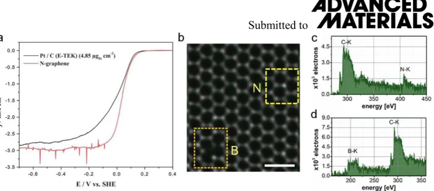
commercial noble metal Pt, as shown in Fig. 7a. The localized defect states induced by the N
dopant atoms are near the Fermi level of graphene, benefiting in the electron transfer from
graphene to the antibonding orbitals of oxygen molecule in the oxygen reduction process[103].
Compared to the two-electron transfer in the pristine graphene, the N-doped system
demonstrates a much more efficient transfer of four electrons in the oxygen reduction
catalysis in alkaline fuel cells[104]. The N-doped graphene electrode yields large steady
catalytic current density with immunity to CO poisoning, superior to the commercial Pt
nanoparticle easily suffering from agglomeration and CO poisoning.
N atoms can be introduced through initial CVD growth[105], solvothermal process[106],
arc-discharge[107] and post-growth annealing of graphene or graphene oxide in ammonia[95, 108,
109]. The substitutional N dopants in the graphene lattice will adopt three configurations[108]:
triple-coordinated graphitic N in a hexagon, double-coordinated pyridinic N in a hexagon,
double-coordinated pyrronic N in a pentagon. And these bonding states of N dopant atoms
present different response to the ORR activity. The report by Geng et al.[95] suggested the
graphitic N species play an important role in the 4e- ORR in alkaline solution. Lai et al.[108]
found that the graphitic N was associated with the limited catalytic current density, while the
pyridinic N improved the onset potential of ORR. The results of Niwa et al.[110] showed that
the ORR activity of the doped graphene with more graphitic N content is higher than that of
doped graphene with more pyridinic edge N, which partially coincides with the DFT
prediction of the much lower energy barrier in graphitic N by Boukhvalov et al.[111]. However,
the lack of comparative investigation on doped graphene with pure graphitic N or pyridinic
edge N hinders a universal and persuasive conclusion on their contribution to the ORR
activity enhancement.
Bangert et al.[112] employed low energy ion implantation to dope monolayer graphene
can be successfully planted into the lattice of monolayer graphene in a high
substitution-to-vacancy ratio by dopants occupying the substitution-to-vacancy defects created. The whole monolayer
structure is mostly hexagonal graphene lattices except dopant impurities, as shown in Fig. 7b.
The annular dark field (ADF) imaging and single atom electron energy loss spectroscopy
(EELS) allows structural and chemical analysis of dopants in graphene including element
assignment and bonding nature[112]. Compared to the uniform ADF intensity of normal carbon
lattice atoms, the B dopant has a darker intensity and the N atom is brighter (in Fig. 7b) as
highlighted in the yellow dashed rectangles. Further spectrum imaging of the rectangular
areas by STEM-EELS confirms the chemical species of both dopants (Fig. 7c,d). The obvious
K-edges of B and N atom and their ADF images demonstrate their substitutional
incorporation into the graphene lattice in a sp2 hybridization. This detection is also an
atomic-scale imaging of graphitic N dopant atom, as mentioned above.
Dual-doped graphene by B and N atoms has been successfully illustrated by Wang et
al.[113] to tailor the band gap of graphene system with much better activity than the Pt/C. The
B, N co-doped graphene was also found by Zheng et al.[114] to exhibit more excellent catalytic
activity with a higher current density and larger onset potential than the single doped
graphene. The dominating pathway of four-electron transfer for oxygen reduction accounts
for the highly-enhanced ORR catalytic performance in the co-doped system.
3. Boron nitride system
Boron nitride (BN) has several crystalline phases: hexagonal, cubic, rhombohedral and
wurtzite with the space groups of P63mmc, F43m, R3m, P63mc, respectively [115]. The cubic
boron nitride is three-dimensional superhard material in a structure similar to the diamond and
thus has the same highest Mohs hardness scale with applications in cutlery and drill[116]. Only
the hexagonal phase BN will be discussed in this paper. Hexagonal boron nitride (BN) is
white in color and has a similar honeycomb graphene-like layered structure, the BN is also
called “white graphite” and used as a lubricant due to its low friction coefficient. Hexagonal
BN is an insulator with an energy gap of 5.8 eV[11] and has extreme chemical stability at high
temperature. Hence BN is often used as a high-temperature insulating ceramic or
corrosion-resistant coating layer, and holds promising potential in graphene-based nanodevices.
3.1 Structural property in BN
As a two-dimensional planar graphene-like structure, atomically thin BN has received
much research interest in its structural and electronic properties since its early preparation[117]
Submitted to
corrected TEM to reveal the hexagonal lattice structure of monolayer BN and directly
discriminate the chemical species. As shown in Fig. 8a, single B vacancy can be easily
distinguished in the HRTEM imaging of BN monolayer. Krivanek et al.[39] further employed
quantitative ADF imaging for atom-by-atom structural and chemical analysis of BN
monolayer containing C and O dopants (Fig. 8b). Each atom was unambiguously resolved and
identified. Under the electron beam irradiation, point defects such as single boron
vacancies[12] will be preferentially generated even at low voltage 80 kV. Continuous electron
bombardment to the BN monolayer leads to the aggregation of boron vacancies to form
triangular holes composed of three equivalent N-terminated zigzag edges. Similar
experimental observation of zigzag edges formed at 120kV was reported by Meyer et al.[118].
The initial formation of single B vacancy has a three-fold symmetry and these gradually
transforms into triangular holes under beam irradiation due to the asymmetric beam damage
mechanism of the two distinctive sublattice in BN thin film. Alem et al. observed both zigzag
and armchair edges in the BN nanosheet[119]. No vacancy reconstruction is found in the
monolayer system, indicating the instability of B-B or N-N bonds in this 2D lattice of BN.
Alem et al.[120] visualized the structural Jahn-Teller distortion of single point vacancies in
BN bilayer system via ultra-high resolution TEM where both spherical and chromatic
aberrations are corrected. The sub-• resolution image with a high signal-to-noise ratio show
convincingly the local lattice distortion of the individual point defects. Figure 9a shows the
exit-wave-reconstructed phase of a bilayer BN with the inset manifesting the image of a boron
monovacancy (VB) in either the bottom or the upper layer of the BN bilayer. Instead of the
expected threefold p3 symmetry for the VB vacancy, the experiments (shown in the inset of
Fig. 9a) revealed a reduced pm symmetry due to the B-N bond reconstruction between layers
caused by the Coulomb repulsion of the highly negative charge in the defect site. The DFT
calculated structure of single boron vacancy in a BN bilayer has an obvious distortion from
the three-fold symmetric structure, as shown in Fig. 9b, e. The experimentally reconstructed
phase of the exit wave function coincides quantitatively with the simulated phase (Fig. 9c, d, f,
g). The nearest-neighboring N lattice atoms around B vacancy get bonded with the B lattice
atoms in the other layer, thus the B-N bonds are reconstructed between layers. This study is
also important example of the advancement in the measurement of the three-dimensional
structure distortion of single defects in combination with DFT simulation, in picometer-scale
accuracy.
The sites neighboring single vacancies preserve remarkably different chemical bonding
and coordination environment compared to the faraway normal lattice sites, thus leading to
unique electronic states. The detection of ELNES in the core loss EELS can be used to
analyze the unoccupied electronic states of novel nanostructures or single point defects at the
single atom level and sensitivity.
3.2.1 Electronic states probed by TEM
Suenaga et al.[121] combined ADF imaging and EELS-ELNES in an aberration corrected
STEM to investigate the electronic properties of N atoms around the vacancy and N atoms
from the normal sublattices. Although the delocalization effect of EELS signal is inevitable
and limits the atomic-resolution chemical mapping of BN sublattices, the STEM-EELS
technique still provides an easy access to the density of empty electronic states of the target N
atom. Figure 10 a,b shows the ADF image of a BN monolayer with a B monovacancy and the
structural model in Fig. 10c shows the chemical coordination environment. The EELS line
profile conducted along the yellow arrow in Fig. 10b crosses the normal triple-coordinated N
atoms “1 and 3” and unsaturated double-coordinated N atom “2”. The K-edge fine structures
of each N atom are presented in Fig. 10d with the common r, peak at 401 eV, resulted from
the 1s r,transition. A prominent prepeak at 392 e↑ appears on the unsaturated N atom “2”,
which is highlighted in yellow. The structure of B vacancy indicates that this prepeak may be
signature of the dangling bonds of three N atoms around B vacancy[121]. As shown in Fig. 10e,
the DFT simulated ELNES spectra of normal N atom and unsaturated N atom around B
vacancy show the obvious chemical shift of r, peak in the vacancy case, highlighted by the
arrow head. The dangling bonds of N atoms is calculated to have unoccupied molecular
orbital with lower energy than that of the normal triple-coordinated N sublattice, thus giving
rise to lower 1s r,transition energy and behaving as a sharp prepeak at 391.7 eV. Contour
maps of the electronic states of the double-coordinated N atom in Fig. 10f display the spatial
distribution of the occupied deep-level 1s state and the 2p state at the lowest unoccupied
molecular orbital (LUMO). The 1s state deviates from the well-known spherical shape and
seems to be attracted towards the vacancy center and the 2p state gets closer to this center.
Three such equivalent N atoms do make contribution to the core-level transition as an obvious
prepeak in the K-edge spectrum.
Compared with previous identifications of the chemical species of BN monolayer simply
by quantitative ADF imaging or HRTEM phase reconstruction, Suenaga et al. provides a
more direct evidence for the atom-by-atom structural and chemical analysis by mapping the
Submitted to
3.2.2 Electronic structure and single photon emitter
The introduction of vacancies into BN monolayer system will lead to localized defect
states in the intrinsic band structure. Huang et al.[122] employed first principle calculations to
show the in-gap defect level in the electronic structure, as shown in Fig. 11a,b. for the relaxed
structure of vacancies VB, VN and VBN. The corresponding schematic electronic structure is
presented in Fig. 11b. The vacancy VB has a Jahn-Teller distortion with its symmetry
lowering from D3h to C2v. And two of the neighboring N atoms have the same spin direction,
in antiparellel coupling with the spin of the third N atom, hence the distribution of magnetic
moment of the neighboring N atoms in VB is 1, 1, -1 B, respectively. Defect states of VB are
complicated owing to the crystal field splitting and spin exchange splitting, resulting in one
spin-up state moving down into valence band. The other three hole levels above valence band
maximum indicate charge-neutral VB is a triple acceptor, as shown in the left of Fig. 11b.
While for vacancy VN, the structure remains three-fold symmetric (D3h) with the total
magnetic moment of 1 B from the three neighboring B atoms in the same spin direction[122].
The VBN has a C2v symmetry and the spin is unpolarized, thus VBN is nonmagnetic. For VBN,
the electronic structure in the right of Fig.11b imply that all the in-gap defect states are empty
and high in energy and thus VBN behaves as deep acceptors if in a charge neutral state.
The localized defect states induced by vacancies in BN may lead to novel physical
properties such as nanophotonic emission[123, 124]. Tran et al.[125] showed a polarized and
intense single-photon emission in hexagonal BN at room temperature (Fig. 11c). The photon
energy of the excitation laser at 532nm (~2.3 eV) was much smaller than the gap of BN (5.8
eV) and thus excitation of the defect states within the gap can be expected. The brightest
emission was found at 623nm (1.99eV) and localized within the atomically thin layers (see
emission mapping in the Fig. 11c inset), together with other weak emission doublets at longer
wavelength (1.99eV~1.79eV). The time-resolved fluorescence measurement of the brightest
emission shows a lifetime of 3ns as well as its antibunching nature consistent with the
characteristic of a single photon emitter. Linearly polarized dipole transition was also verified
for this quantum emitter by excitation emission polarization measurements. This linear
polarized dichroism actually reflects the highly anisotropy of the defect structure involved.
Among the possible intrinsic vacancy defects (VB, VN, NBVN), the DFT calculations further
support the anisotropic antisite-vacancy complex NBVN (N replaces one neighbouring B
around VN, Fig. 11c right inset) could be most likely defect responsible for the intense
sub-bandgap quantum photonic emission in BN. The origin for other weak emissions
3.3 Magnetic properties of dopant defects
Ideal monolayer hexagonal BN is a nonmagnetic material, similar to graphene. Doping
transition metal atoms to occupy the vacancy sites of BN monolayer system is shown to be a
theoretical possibility for chemical decoration and local magnetism. Exploring different
transition metal dopant atoms is also necessary for designing magnetic and even catalytic[126]
applications of BN nanosheets from the single atom perspective.
Huang et al.[122] calculated the relaxed structure of different transition metal adsorbates
on the vacancy sites of VB, VN and VBN in monolayer BN, as shown in Fig. 12a. The binding
energy of transition metal atoms on VB is obviously larger than that on VN and VBN (in Fig.
12b), which could be induced by a large charge transfer between metal atom and
nearest-neighboring N atoms around VB. And the geometry of absorption structure of each metal atom
in Fig. 12c can be understood by the structure and charge distribution. Metal atoms on VBN
have a smallest height above the BN monolayer surface due to the largest empty space of the
defects for the accommodation of the transition metal adatoms. The height of metal atoms on
VB is smaller than that on VN due to the negative charge state of neighboring N atoms in VB.
In the theoretical calculations[122] by Huang et al., the total magnetic moment for the
adsorption structures of single transition metal atoms on the vacancy sites is shown in Fig.
12d. For the case of vacancy VB, the metal adatom transfers three electrons to the three in-gap
hole states of VB and itself becomes a metal ion in a +3 valence state. All the transition metal
atoms are in the high-spin state because the exchange splitting is larger than the crystal field
splitting except for Fe, Co, Ni. In the case of Fe, Co, Ni adsorption on VB site, the large
crystal field splitting results in a low-spin state, for instance, d3 d2 for Fe3+. By increasing the
height of the adatom above the BN monolayer surface or applying an external electric field,
the magnitude of crystal field splitting energies can be reduced. Thus the Fe adatom on VB
will undergo a ‘spin crossover’ from low-spin state to high-spin state, and this spin transition
has been manipulated through spin-polarized STM experiments[127]. In the adsorption on V BN,
two electrons of the metal atom (M) transfer to the in-gap states of VBN and yield a M2+ ion.
The remaining valence electrons obey Hund’s rules, resulting in the total magnetic moment’s
linear relation with the atomic number Z (blue curve in Fig. 12d). For the metal adsorption on
VN, the electron arrangement is quite complex and differs from that on VB and VBN, due to the
hybridization of in-gap defect states of VN and valence electron states 4s, 3d of metal ligands.
Different spin configurations lead to various magnetic moments in the metal adsorption on VN.
As an important theoretical prediction for a doped BN monolayer, the nanomagnetism
spin-Submitted to
polarized STM at the single atom level[128-131]. As the ‘spin crossover’ and magnetic states
can be manipulated by varying the relevant crystal filed of vacancy defects as well as the
external electric field[132], they could have applications in external field driven memory
devices. The research into macroscopic scale magnetism in BN system should focus on valid
defect engineering and the development of large-scale magnetic decoration.
3.4 Band engineering by carbon doping
Doping impurity atoms in individual vacancy defects tailors the electronic structure
locally and plays a limited role in the change of the macroscopic properties, unless this doping
can reach a relatively high level. For traditional silicon semiconductors, a quite low doping
level ~ 10-6 is enough to considerably change the electric conductivity. However, in insulating
BN system, heavy doping to a high level will be needed to transform its electric properties.
Monolayer BN has a single-atom-thick honeycomb structure similar to graphene with
almost the same lattice parameters. The substitution of B or N by C atoms will not induce
obvious lattice mismatch, thus carbon doping in BN monolayers yields coherent hexagonal
BCN nanosheests. A transition from insulator to conductor after adequate doping was
predicted by many theoretical calculation[133, 134] and observed experimentally[135] in the BN
nanostructures such as nanosheets, nanotubes and nanoribbons.
3.4.1 Early researches on BCN bulk system
Watanabe et al.[136] measured the hall effect of chemical vapor deposited BC
2N thin film,
and found it’s a p-type semiconductor and its acceptor level is shallow, at between 5.5 meV
and 23 meV. Later spectroscopic measurements by scanning tunnelling microscopy[137]
revealed a characteristic optical gap of 2 eV, which is further verified by the low temperature
photoluminescence spectra showing a 600 nm peak at 4.2K. Furthermore, the
density-of-states of the occupied valence band measured by X-ray photoemission spectroscopy (XPS)
shows a threshold energy of 0.95 eV valence band maximum locates above Fermi level. It can
be deduced that the band gap must be larger than 1.9 eV, since the Fermi level is located
almost in the middle of the gap but closer to the valence band extreme in a p-type
semiconductor.
Chen et al.[138] remeasured the band structure of BC
2N thin film by angle-resolved
electron energy-loss spectroscopy (EELS) in a STM high vacuum system. The band gaps at
different parallel momentum transfers are derived from the onset energies of the low loss fine
structures. Measurements of band gaps as a function of momentum transfer present a
From the experiments by Watanabe et al. and Chen et al., the bulk BC2N material is an
indirect semiconductor with an indirect gap of 1.4 eV. The direct optical transition in bulk
BC2N has an energy of 2 eV, consistent with previous observations of a vertical gap by
photoluminescence and XPS[137] and with the DFT calculation by Liu et al.[134].
3.4.2 Recent advancement in monolayer BCN system
Mazzoni et al.[133] systematically predicted the electronic structure and energetics of
B-C-N hybrid graphene-like structures by first principle calculations. The formation energy of
different configurations show that the structure with a sequence of zigzag C-C bonds is the
most stable and no B-B or N-N bonds are favored. In the carbon-rich structure of BC2N, the
lowest formation energy lies in the configuration with the maximum of the number of B-N
and C-C bonds, indicating a tendency towards island-like structures in segregated phases[133].
The electronic structures of the considered BCN configurations show a wide range of band
gaps from zero to 2.5 eV. And some metallic structures are calculated to preserve relatively
low formation energy. An insulating, semiconducting to metallic transition is therefore
predicted with the increasing addition of carbon into the BN system. It is found that the hybrid
structure with large band gap generally have the higher stability and is usually correlated with
the chemical stoichiometry ratio of B/N ~1. In other words, under thermal equilibrium
condition, the large-bandgap structure in segregated phases with maximum zigzag C-C bonds
and B-N bonds is the most stable BCN hybridized system. The first-principles DFT
calculations by Mazzoni et al. predict theoretically the separated BN and graphene domains in
the carbon doped BN system[133].
Ci et al.[139] first synthesized two-dimensional hexagonal monolayer hybridized BCN
through chemical vapor deposition. Almost no substitutional doping of B or N into graphene
lattice occurs in this hybrid system. The ultraviolet visible absorption spectra of hybridized
BCN atomic layers present two peaks corresponding to pure graphene and BN, confirming
that this BCN system was phase-segregated with BN and graphene domains randomly
distributed. Furthermore, the domains are expected to be larger than a few nanometers to
screen the effect of short-period superlattice that makes a semiconductor. The optical response
of BCN atomic layers preserves both properties of graphene and BN. In their electric
measurements, the highly carbon-doped hybridized atomic layers present the electric
resistance increasing dramatically as the temperature decrease, which is the characteristic of a
semiconductor, indicating the graphene domain contribute to the insulating-semiconducting
transition[139]. However, other groups found ternary alloy BCN near the domain boundaries of
high-Submitted to
temperature growth[141]. This is inconsistent with the previous theoretical prediction of the
C/BN immiscibility by Yuge[142], and the contrasting experimental reports remain a
controversy.
3.4.3 In-situ doping in TEM
Wei et al.[135] employed in-situ TEM to observe the doping effect of carbon in BN
monolayer nanosheet, as shown in Fig. 13. They proposed a post-synthesis route[143] by
utilizing the electron beam irradiation effect to create B or N vacancies for subsequent doping
by carbon atoms decomposed from the hydrocarbon molecules intentionally introduced into
the TEM. In this way, the BN monolayer can be completely transformed into conducting
carbon system, and the intermediate state is semiconducting and magnetic BCN nanosheet. In
Fig. 13a, the selected area electron diffraction of the doped BN nanosheets confirms the
hexagonal lattice after long-time irradiation. During the continuous irradiation-damage
assisted carbon doping, the chemical analysis was conducted by electron energy-loss
spectroscopy and spatially resolved energy filtered TEM mapping. The comparison of the
core loss EELS before and after irradiation in Fig. 13b indicate the successful doping of
carbon atoms and the obvious r*peaks at 284 eV mark the introduction of carbon in sp2
hybridization. Energy filtered TEM image of B and C elements in Fig. 13c,d shows the
enrichment of carbon atoms in central particular sites of the BN nanosheet, which hints the
segregation of carbon phase domains. The in-situ electric transport measurements in Fig. 13e
shows that the pristine BN is insulating and the doped BN nanosheets become conducting.
And also the electric conductivity increases obviously with the irradiation time, indicating a
transition[135, 143] from insulator, semiconductor to conductor, which is in good agreement of
previous theoretical predictions on BCN system. This in-situ experiment by Wei et al.
demonstrated an effective and precise control of electric and magnetic properties of
two-dimensional nanosheets through irradiation-assisted doping of carbon.
3.4.4 Band edge excitation of BCN monolayer by EELS
Arenal et al.[144] employed spatially-resolved STEM-EELS to study the bandgaps of
single-wall and double-wall BN nanotubes. The low-loss electronic excitations of all
nanotubes show a threshold at ~5.8 eV, which is an independent nonoptical measurement of
the wide gap of BN nanostructures. Pan et al.[145] investigated the electron energy-loss
spectroscopy of BN nanosheets with different thicknesses and found unique extra electronic
excitations in the monolayer below its band gap threshold 5.8 eV. As shown in Fig. 13f, the
atomically-resolved ADF image of a BN monolayer shows abnormal intensities at some
intensity analysis discriminates the chemical species of dopants such as C atoms (in yellow),
O atom (in dark blue) from the normal B (light blue) and N (gray) atomic sublattices. Based
on this atomic model in Fig.13f, the DFT has been used to calculate the low-loss spectrum (by
WIEN2K package) which is shown as the black solid curve in Fig. 13g. This is to be
compared with the experimental low-loss spectrum shown as the gray curve. Two obvious
peaks at 6.3 eV and 14.3 eV are the typical r , u plasmon resonance of the BN monolayer.
Low-energy pre-peak extends to 3 eV on the shoulder of the r plasmon peak, and this
pre-peak structure appears only in some localized regions. Another shoulder structure at 7.5 eV on
the high-energy side of the r plasmon peak was also only selectively observed. These
abnormal low-loss fine structures[145] are believed to be associated with defects inside, which
can be inferred from the fact that only a few localized regions give these preplasmon or
postplasmon shoulder structures. This has been collaborated by the quantitative ADF imaging
and impurity atom assignment in Fig. 13f. Correspondingly, the calculated spectrum is
consistent with the experimental low-energy preplasmon structure, as indicated by the blue
arrows in Fig. 13g. The local substitution of carbon atoms in BN sublattices corresponds to
moderate doping, which make the electronic excitation extends to lower energy region of the
spectrum, suggesting the transformation into a semiconductor. This EELS measurement by
Pan et al. presents another non-optical and nonelectric experimental approach for the
checking of the insulator-to-semiconductor transition through electronic structure engineering
by carbon substitutional doping in monolayer BN.
4. Transition metal dichalcogenides (TMDs)
Among the two-dimensional graphene-like materials, layered transition metal
dichalcogenides (TMDs)[24, 146-148] have recently also attracted extensive research interest in
their atomic structure, unique electronic and optical properties, electric transport because of
its great significance in valleytronics[149-152] and electronics[23, 28, 153] application. As a typical
TMDs family, - group MX2 (M = Mo, W; X = S, Se) has three types of crystal phases:
1T phase as a metal; 2H phase and 3R phase as semiconductors. Among these polymorphs,
hexagonal MoS2 in 2H phase has already been investigated widely in materials research and
in industrial applications[154] of lubricants and hydrodesulfurization catalysts. As a
representative of TMDs, MoS2 has many structure, electronic, optoelectronic and catalytic
properties similar to other TMDs-MX2. Hence we mainly focus on MoS2 to limit the scope of
this section, where most contents are also applicable to other - group TMDs.
Submitted to
Monolayer 2H-MoS2 has a sandwiched structure in a trigonal prismatic coordination
formed by covalent bonding between Mo and S atom layers. The basic skeleton of single
layer MoS2 are assembled into its bulk counterpart through interlayer van der Vaals
interaction and specific interlayer stacking sequence, similar to h-BN and graphite. The
layered nature of the bulk MoS2 makes interlayer sliding easily happen when it’s subject to
external friction, therefore they are often used as lubricants. In addition, large interlayer
separation provides enough space for mass transportation of small molecules in the interlayer
channels with high specific surface area, thus there is considerable potential for applications
in lithium ion battery[155, 156] and hydrogen storage[157].
Since the weak van der Waals interaction between layers, micromechanical exfoliation[17,
158], liquid-phase ultrasonic dispersion[159] were widely employed to prepare MoS
2 atomic
layers. Laser[160] or plasma thinning[161] has also been adopted to obtain few layers from thin
flakes. However, these top-down methods are impractical for the scalable production.
Solutions such as chemical/physical vapour deposition enable wafer-scale production of
monolayer or few-layer MoS2 nanosheets. For the CVD growth approach, ammonium
tetrathiomolybdate[162, 163] (NH
4)2MoS4 can be decomposed in Ar+S gas at a temperature
1000 to form MoS2. Molybdenum oxides[164-166] (MoO3, MoO2) can also be reduced to
MoS2 under the flow of S vapor. So far, synthesis of large area high quality MoS2 by CVD
provides a very effective way for its electric and optoelectronic application.
The most attractive physical properties of layered MoS2 lie in the thickness-dependent
behaviour of its optical, electronic transport and optoelectronic properties which are deeply
rooted in the electronic band structure. Interesting quantum confinement effect[13, 158] appears
in the form of a crossover[167] from the indirect to a direct gap semiconductor when the layer
number of MoS2 decreases from bulk to monolayer. From multilayer to bilayer, the MoS2
present an increasing indirect bandgap from ~1.3 eV to ~1.6 eV. In the monolayer limit, MoS2
has been reported to behave as a direct semiconductor[158] with a bandgap 1.8 eV, indicating
its potential application in optoelectronics and photovoltaics[147, 168, 169]. Besides, the
monolayer MoS2 lacks an inversion symmetry that is present in the multilayer’s crystal
structure, leading to different interband transition selection rule in the vicinity of K and K’
points of the first Brillouin zone, giving rise to valley contrasting circular polarization
dichroism[149-151, 170]. This valley dependent dichroism has also been identified in the
electroluminescence measurements[171].
Monolayer MoS2-based field effect transistors[28] show a high current on/off ratio ~1!108,
exfoliated MoS2 monolayers have been utilized to fabricate FET devices to detect
environmentally detrimental gas NO[172] with a high sensitivity up to 0.8ppm. Most MoS 2
nanosheets used as the channel material in FETs are n-type semiconductors, and the origin of
this doping character is still unclear with some research suggesting either S vacancies or
impurity atoms[173].
Surface adsorbates, intrinsic structural defects[174] such as point defects, dislocations and
grain boundaries, and edge structures are all considered as important causes for the low
mobility of charge carriers in electric transport and highly enhanced catalytic activity.
Plentiful efforts have been taken to identify these nanostructures by recent atomically
resolved transmission electron microscopy. Atomic defects such as vacancies[174] (pristine)
and grain boundaries[164, 165] have been discovered in monolayer MoS
2 prepared by CVD
growth. Wang et al. have synthesized MoS2 nanoribbons[175] encapsulated in carbon
nanotubes. For nanoribbons, the armchair type presents a width-dependent semiconducting
gap, while the ferromagnetic zigzag nanoribbons are always metallic regardless of the width
[176, 177]. For consistency with the above sections, we will only discuss the defects in atomic
size including point defects, adatoms and impurity dopants in monolayer MoS2 system and
show how they tailor the electronic, magnetic and catalytic properties.
4.2 Point defects in MoS2
Direct semiconducting property with a proper bandgap of 1.8 eV makes monolayer MoS2
a proper candidate in field effect transistors, integrated logic circuits, photodetectors, gas
sensors and flexible optoelectronic or plasmonic devices. The widely-adopted synthesis of
MoS2 atomic layers by chemical vapor deposition[166, 178] help to bridge the gap between
large-scale high-quality crystal growth and the nanoelectronic applications. However, the
obtained electron mobility[179] of MoS
2 is much lower than that of the mechanically exfoliated
counterparts[180]. Furthermore, all experimentally reported electron mobilities of CVD, PVD
or mechanically-exfoliated MoS2 have almost one order of magnitude lower than its
theoretical limit[181] of 410cm2V-1s-1. Such large discrepancies are widely believed to arise
from charge carrier scattering centers such as point defects, grain boundaries, surface
adsorption, dangling bonds or Coulomb impurities. These defects are common in any crystal
materials, and have been thoroughly investigated in traditional Si or GaN semiconductors as
they play a crucial role in the electric and optical properties[49].
Zhou et al.[174] gave a systematic characterization of intrinsic atomic defects in CVD
grown MoS2 by atomic resolution annular dark field (ADF) imaging in an aberration