Rochester Institute of Technology
RIT Scholar Works
Theses Thesis/Dissertation Collections
2009
Gate-to-channel parasitic capacitance minimization
and source-drain leakage evaluation in germanium
PMOS
Raymond T. Krom
Follow this and additional works at:http://scholarworks.rit.edu/theses
This Thesis is brought to you for free and open access by the Thesis/Dissertation Collections at RIT Scholar Works. It has been accepted for inclusion in Theses by an authorized administrator of RIT Scholar Works. For more information, please [email protected].
Recommended Citation
Gate-to-Channel Parasitic Capacitance Minimization and
Source-Drain Leakage Evaluation in Germanium PMOS
By
Raymond T. Krom III
A Thesis Submitted
in Partial Fulfillment
of the Requirements for the Degree of
Master of Science
in
Microelectronic Engineering
Approved by:
Prof. _______________________________ Dr. Santosh K. Kurinec (Thesis Advisor)
Prof. _______________________________ Dr. Sean L. Rommel (Committee Member)
Prof. _______________________________ Dr. James E. Moon (Committee Member)
Jerome M. Mitard (IMEC Collaborator) Dr. Marc Heyns (IMEC Collaborator) Dr. Marc Meuris (IMEC Collaborator)
DEPARTMENT OF MICROELECTRONIC ENGINEERING
KATE GLEASON COLLEGE OF ENGINEERING
ROCHESTER INSTITUTE OF TECHNOLOGY
ROCHESTER, NEW YORK
ii
NOTICE OF COPYRIGHT
© 2008
Raymond T. Krom III
REPRODUCION PERMISSION STATEMENT
Permission Granted
TITLE:
“Gate-to-Channel Parasitic Capacitance Minimization and Source-Drain Leakage Evaluation in Germanium PMOS”
I, Raymond T. Krom III, hereby grant permission to the Wallace Library of the Rochester Institute of Technology to reproduce my thesis in whole or in part. Any reproduction will not be for commercial use or profit.
iii
Abstract
This work studies the behavior of both gate-to-channel capacitance (CGC) and
source-channel-drain/well leakage in metal-gate/high-κ/Ge PMOS technology
(W = 10 µm and L = 10; 5; 1 µm) under development at IMEC. The hole drift-mobility of
germanium is ~4X that of silicon, leading researchers to evaluate germanium as a
possible channel material replacement for PMOS expected at the 32 nm technology node.
In particular this study focuses on—but is not restricted to—(1) the presence of a
parasitic gate-to-channel capacitance (CGC), the large non-ideal trap assisted conductance
which contributes to it, and its function versus Ge-PMOS architecture and gate length; (2)
the existence of C-V tool compensation error due to CGC measurement technique resulting
in conductance measurement error; (3) the presence of large source-channel-drain/well
leakages characterized using a new MOS gated-diode measurement technique; (4)
extrinsic capacitance (CEXT), flatband voltage (VFB), and effective oxide thickness (EOT)
parameter extraction with discussion on inversion layer quantization.
This study found that excessive current leakages from the Ge-PMOS
source-and-drain into the channel led to a chuck-dependent parasitic capacitance during CGC
measurement. This excessive leakage is identified as a trap-assisted leakage through both
AC and DC analysis. The chuck-dependent parasitic capacitance was an unexpected side
effect of the PMOS architecture: namely the lack of N-Well isolation. The parasitic
capacitance—dependent on both applied bias and frequency—was separated into two
main capacitive components: a frequency-dependent source/well and drain/well
iv
junction leakage capacitance (CPara_GIJL). A third parasitic capacitance due to interface
trap (IT) contribution (CIT) during channel depletion was also identified.
This study also found that the new MOS gated-diode measurement technique
designed to separate and evaluate the source, channel, and drain leakage components is
superior to typical VGS versus IDS methods when attempting to quantify the CGC
measurement. The MOS gated-diode configuration allowed for temperature-dependent
analysis and activation energy extraction (EA), thereby providing a means to confirm
individual leakage components: diffusion; Shockley-Read-Hall (SRH); trap-assisted
leakage (TAL). TAL components include: Poole-Frenkel (PF); phonon-assisted tunneling
(PAT); trap-to-band tunneling (TBT).
In conclusion, it was found that the source-channel-drain/well leakages and hence
parasitic capacitances of PMOS built on relaxed germanium-on-silicon can be minimized
by reducing the source/drain area, reducing the source/drain-to-gate contact distance,
while increasing both the gate length and measurement frequency. The dominance of
SRH and TAL during Ge-PMOS operation disagrees with diffusion dominance predicted
by theory and as a result opens the door for future research. Future research includes
Ge-PMOS fabrication on substrates free of dislocations—to minimize SRH and TAL current
v
“The solution is not to be found in the result achieved, but
in the way of achieving it.”
vi
Acknowledgement
This research is a team effort that came to light through the assistance and
dedication of a number of people. I would like to thank first and foremost Dr. Santosh K.
Kurinec, who not only provided her guidance and moral support, but also provided the
author with the National Science Foundation (NSF) International Research and Education
Experience (IREE) opportunity (grant number EEC – 738337). Through this grant the
author was able to travel to IMEC located in Leuven Belgium, research their
state-of-the-art Germanium PMOSFET technology, and absorb the Belgian/European culture. If one
thing must be said, it is that this research is greater in both scope and depth due to her
constant mentorship.
IMEC is a world-leading independent research center addressing the next
generation of processes, chips, and systems utilized in nanoelectronics and
nanotechnology areas. Housing state-of-the-art 300 mm and 200 mm clean rooms
extended in 2006 for electrical characterization, IMEC is evaluating Ge—among other
materials—as a channel replacement material for PMOSFET and other advanced
technologies expected at the 32 nm technology node. Research at IMEC provided the
author with a great degree of resources, flexibility, and creative freedom. The author is
extremely grateful to this research center, its employees, faculty, and vision.
At IMEC, Dr. Marc Heyns’ support was invaluable. Besides sponsoring the
author, his leadership and professionalism provided the author with the means of
grounding. Jerome M. Mitard’s perspective, support, and superb guidance are greatly
vii
PMOSFET technology. The author thanks Guy Brammertz for being a mentor, helping
the author acclimate to the IMEC environment, and providing a perspective on electrical
test through testing InGaAs dot capacitors. Dr. Geert Eneman was essential for he
pointed the author in the right direction when identifying gate-induced-drain leakages.
The author is greatly thankful to the entire Germanium/III-V/EPI groups. Their passion
for research and life, as well as their ability to communicate and share information are
deeply respected- thank you.
The author thanks Dr. Sean L. Rommel for his superb insight into both
germanium and III-V semiconducting technology as well as our many conversations on
the future of aspect-ratio-trapping technology. The author thanks Dr. James E. Moon for
all his support and guidance, as well as imparting a unique perspective when accounting
for classical and non-classical behaviors in Advanced MOSFET technology.
The author thanks the friendship and support of Jacque, Mike, Jared, Joel, Dave,
Bob, and Kris. The author thanks family: for all you have sacrificed for me and continue
to do, I am completely grateful. Finally, the author would like to acknowledge the
support provided by RIT and the NSF grants EEC-530575; ECCS-0725760 that allowed
viii
Table of Contents
Title Page ... i
Library Release ... ii
Abstract ... iii
Acknowledgement ... vi
Table of Contents ... viii
List of Figures ... xi
List of Tables ... xiii
List of Symbols and Abbreviations... xiv
Chapter 1: Introduction and Motivation ...1
1. The 32 nm Technology Node and Germanium PMOS ...1
1.1.Silicon, Germanium and III-V ...3
1.2.Present Study: Relaxed Germanium-on-Silicon ...5
1.2.1. Architecture Modules D1, G3, J2 ...8
1.3.Statement of Problem and Thesis Contribution ...9
1.4.Organization of Thesis ...13
Chapter 1: References ...15
Chapter 2: PMOS Gate-to-Channel Capacitance (CGC) Equipment/Measurement ...16
2. Introduction ...16
2.1.C-V Equipment and Configuration ...17
2.2.Measurement of Capacitance and Conductance ...21
2.2.1. Auto Balancing Bridge Method ...22
2.3.Purpose of CGC, Regions of Operation, and Ideal Behavior ...24
2.3.1. Connection to Generic PMOSFET ...25
2.3.2. High Accumulation and High Inversion ...27
ix
Chapter 3: Germanium PMOS CGC Measurement ...31
3. Introduction ...31
3.1.Conductance Method ...32
3.2.CGC Measured Regions and Observed Behavior ...34
3.3.Parasitic CGC Chuck Dependence ...37
3.4.Parasitic CGC Source and Drain Geometry Dependence ...40
3.5.Parasitic CGC & Conductance versus Architecture ...42
Chapter 3: References ...48
Chapter 4: CGC Technique Affecting Conductance ...49
4. Introduction ...49
4.1.Grounding Germanium Substrate ...50
4.1.1. Negative Conductance-Capacitance Effect ...54
Chapter 4: References ...56
Chapter 5: Germanium PMOS Source-Drain Leakage ...57
5. Introduction ...57
5.1.Transistor Leakage Mechanisms...58
5.1.1. P/N Junction Reverse Bias Leakage (I1) ...60
5.1.2. Surface Generated Leakage (I7) ...64
5.1.3. Gate Induced Drain Leakage (I5) ...66
5.2.MOS-Gated-Diode and Expected ...69
5.3.Experimental Results ...70
5.3.1. Source/Drain-to-Well Reverse Bias Leakage (2I1) ...70
5.3.2. Gate Induced Junction Leakage (2I5) ...72
5.3.3. MOS-Gated-Diode Results ...73
5.3.4. Activation Energy Extraction ...76
x
Chapter 6: Ge PMOS CGC Parameter Extraction ...83
6. Introduction ...83
6.1.Extrinsic and Intrinsic Capacitance Non-idealities ...83
6.1.1. Extrinsic and Intrinsic Capacitance Extraction of J2 ...85
6.2.Effective Oxide Thickness (EOT) Calculation of J2 ...88
6.2.1. Inversion Layer Quantization ...89
Chapter 6: References ...91
Chapter 7: Conclusion Section...92
7. Conclusions ...92
xi
List of Figures
Fig. 1.1: Intel’s 2006 device trend-projection ...2
Fig. 1.2: Ge PMOSFET ...7
Fig. 1.3: Ge PMOS source/drain contact and gate contact layout ...8
Fig. 1.4: Gate-to-Channel Capacitance (CGC) for two ~10 µm x10 µm pMOSFETs ...10
Fig. 2.1: A SUSS Microtec. semiautomatic probe station PA300PS ...18
Fig. 2.2: Front Panel of the Agilent 4284A 20Hz-1MHz Precision LCR Meter ...19
Fig. 2.3: Impedance (Z) and admittance (Y) representations ...21
Fig. 2.4: Auto-Balancing Bridge Method impedance measurement ... 23
Fig. 2.5: Standard CGC connection and measurement for PMOS ...26
Fig. 2.6: Components of high accumulation and high inversion capacitance ...27
Fig. 3.1: Equivalent circuit for parallel conductance measurements ...32
Fig. 3.2: CGC for a 10 µm x 10 µm Ge PMOS device (D1) ...35
Fig. 3.3: Normalized conductance (G/ω) for Ge PMOS (D1) ...36
Fig. 3.4: Parasitic CGC removal for a 10 µm x 10 µm Ge PMOS device (D1) ...37
Fig. 3.5: Difference of CGC 1 MHz & 100 kHz (Float-Ground) ...38
Fig. 3.6: Absolute current leakage from front-side well contact to chuck ...39
Fig. 3.7: Difference of CGC 1 MHz & 100 kHz breakdown into CPara1 & CPara2 ...40
Fig. 3.8: Minimization of CGC Parasitic Capacitance ...41
Fig. 3.9: Extrinsic and parasitic capacitance J2 comparison with Si POR ...42
Fig. 3.10: Capacitance and conductance measurement of D1 architecture ...43
Fig. 3.11: Capacitance and conductance measurement of G3 architecture ...45
Fig. 3.12: Capacitance and conductance measurement of J2 architecture ...46
xii
Fig. 4.2: Ranging function present to measure impedance from low to high values ...53
Fig. 4.3: Difference calculation for (a1) G/Aω and (a2) CGC ...55
Fig. 5.1: The six transistor current leakage mechanisms ...59
Fig. 5.2: The three primary transistor current leakage mechanisms ...60
Fig. 5.3: Electron energy band diagram for Ge with deep-level impurities ...65
Fig. 5.4: Electron generation mechanisms ...66
Fig. 5.5: Gate-Induced Junction Leakage versus Gate-Induced Drain Leakage ...67
Fig. 5.6: Three regions of operation for MOS-Gated-Diode leakage ...70
Fig. 5.7: Reverse-bias source/drain-to-well ...71
Fig. 5.8: GIJL of two 10 µm x 10 µm Ge PMOS devices: D1 and J2 ...73
Fig. 5.9: MOS-Gated-Diode configuration showing ID&S-Well leakage and GIJL ...74
Fig. 5.10: MOS-Gated-Diode showing ID&S-Well leakage and GIJL stability ...75
Fig. 5.11: Temperature dependence of ID&S-Well for 10 µm x 10 µm Ge PMOS ...77
Fig. 5.12: Log of JR at VG = 0 V for 10 µm x 10 µm Ge PMOS J2 architecture ...78
Fig. 5.13: Energy extraction at each gate potential ...79
Fig. 6.1: Log of CGC for J2 architecture containing gate lengths of 10; 5; 1 µm ...85
xiii
List of Tables
Table 1.1: Si, Ge, and GaAs selected property comparison at 300K. ...3
Table 1.2: Summary of Ge-on-Si PMOS fabrication...5
Table 1.3: Difference between architectures D1, G3, and J2 ...9
Table 2.1: The three equipment configurations available to measure CGC ...16
Table 3.1: Summary of peak normalized conductance for Fig. 3.10-3.12...47
Table 6.1: Summary of CEXT and VFB from Fig. 6.1 ...86
Table 6.2: Summary of CINV and VINV from Fig. 6.2 ...88
xiv
List of Symbols and Abbreviations
Symbol Unit Description
A µm2 Gate area
ALD - Atomic layer deposition
ω rad/s Angular frequency (2πf)
B S Susceptance
BF2 - Boron difluoride
BTBT - Band-to-band tunneling
CEXT F Extrinsic capacitance
CGC F Gate-to-channel capacitance
CGCO F Intrinsic capacitance
CIF F Inner fringing field capacitance
CIT F Interface trap capacitance
CM F Measured capacitance
CMAT F Material capacitance
CMOS - Complementary metal oxide semiconductor
CO F Outer capacitance
COF F Outer fringing field capacitance
COV F Overlap capacitance
CP F Parallel capacitance
CPara F Parasitic capacitance
CPara_SD F Source/well drain/well leakage parasitic capacitance
CPara_GIJL F Gate-induced junction leakage parasitic capacitance
xv
CTOP F Top capacitance
DIT cm-2eV-1 Interface trap density
DUT - Device under test
E eV Energy difference (trap state vs. conduction band)
∆E eV Poole-Frenkel energy difference
EA eV Activation energy
EG eV Energy gap
εO pF/m Permittivity of free space (8.8542)
Emax V/cm Maximum electric field
ET eV Interface trap level
EMI - Electromagnetic interference
EOT nm Effective oxide thickness
f Hz Frequency
G S Conductance/Susceptance
GIDL - Gate-induced drain leakage
GIJL - Gate-induced junction leakage
GL A Photogenerated recombination-generation current
GP S Parallel conductance
GPIB - General purpose interface bus
HDD - Highly doped drain
HfO2 - Hafnium-oxide
HPC - High probe contacts
I1 A P/N junction reverse bias leakage
I2 A Subthreshold leakage
xvi
I4 A Hot carrier substrate-to-gate injection
I5 A Gate-induced junction leakage
I6 A Punchthrough
I7 A Surface generation leakage in channel
IDS A Drain-to-source current
IMEC - Interuniversitair Micro-Elektronica Centrum
I-V A-V Current voltage measurement
JDrift-Diff A/cm2 Drift-diffusion current density
JR A/cm2 Reverse-bias current density
JSRH A/cm2 Shockley-Read-Hall current density
JSRH_Chan A/cm2 Shockley-Read-Hall current density in channel
κ eV/K Boltzmann’s constant (8.617x10⁻⁵)
KOX - SiO2 dielectric relative permittivity
L µm Gate length
LEFF µm Effective channel length
LMAT H Material Inductance
LPC - Low probe contacts
ML - Monolayer
µeff cm2/Vs Effective carrier mobility
MOSFET - Metal oxide semiconductor field effect transistor
NA cm-3 Acceptor doping concentration
ND cm-3 Donor doping concentration
ni cm-3 Intrinsic carrier concentration
PAI - Pre-amorphization
xvii
PF - Poole-Frenkel
PMOS - P-type metal oxide semiconductor
PMOSFET - P-type MOSFET
POR - Product of record
PVD - Physical vapor deposition
q C Elementary charge (1.602x10⁻¹⁹)
Qi - Inversion charge
R Ω Resistance
RFI - Radiofrequency interference
R-G - Recombination-generation
RP Ω Parallel resistance
RS Ω Series resistance
SRH - Shockley-Read-Hall
SRH - Shockley-Read-Hall
T K Temperature
TAL - Trap-assisted leakage
TBT - Trap-to-band tunneling
TOX nm SiO2 thickness
τS/D_Trap s Time-constant for source/well and drain/well traps
VA V Applied bias
Vbi V Built-in potential
νsat cm/s Saturation velocity
VFB V Flatband voltage
VG V Gate voltage
xviii
VT V Channel threshold voltage
W µm Gate width
X Ω Reactance
Y S Admittance
1
Chapter 1
Introduction and Motivation
1. The 32 nm Technology Node and Germanium PMOS
Since the invention of the semiconducting transistor nearly 60 years ago,
semiconducting technology has grown exponentially in both complexity and application.
To date – and in no small way due to ingenious advancements in fabrication technology –
semiconductors are utilized in nearly every aspect of daily life from telling the time to
using a cell phone. Current research shows, however, that continued growth in this field
will encounter many challenges beyond the 32 nm technology node expected between the
years 2013 and 2015, the solutions to which will require the implementation of both new
materials and advanced non-classical Complementary Metal Oxide Semiconductor
(CMOS) capable of higher drive currents while at the same time minimizing current
leakages and short channel effects [1-4].
At present most state-of-the-art facilities are capable of 65 nm production, with
Intel being the world’s first producer of 45 nm consumer technology [5]. Second to Intel
is AMD currently deploying its 45 nm pilot line, expected to be available in the
second-half of 2008 [6]. These state-of-the-art semiconducting technologies implement process
and global induced strain engineering [5,6], high-κ metal gate stacks [5], and in some
cases—as in the case of AMD’s new 65 nm Barcelona processing technology—SiGe
hybrid source/drain replacement [6]. The replacement of SiO2 as the gate dielectric of
2
To meet device requirements at the 32 nm technology node while maintaining a
foundation in silicon, renewed interest in silicon-compatible germanium p-type Field
Effect Transistor (PFET) and III-V n-type FET (NFET) technologies has begun [1-7]. A
device trend-projection by Intel is shown in Fig. 1.1. Note the advanced non-classical
CMOS technologies currently in use and projected beyond 2008.
Fig. 1.1: Intel’s 2006 device trend-projection adopted from Chau [4]. Note that Intel’s
research projection is more aggressive than that of the ITRS. Intel plans on researching the 32 nm technology node starting 2009 versus 2013 for ITRS [2].
Most important to such technology and the main focus of this study, are the methods used
to characterize their electrical operation. This study focuses on IMEC’s Ge-PMOSFET
technology and reveals that one must quantify source-drain-channel leakage and its effect
on Gate-to-Channel Capacitance (CGC) before using CGC to extract critical device
parameters.
This figure is reprinted by permission of Intel Corporation,
[image:21.612.118.531.204.461.2]3
1.1. Silicon, Germanium, and III-V
As was briefly mentioned, researchers are interested in Ge and III-V materials for
the next generations of semiconducting technology. Such materials provide an extra
degree of freedom—mobility enhancement—in the manufacturing of complex
semiconducting technologies. With such freedom come complexities such as
characterization, fabrication, and integration of these advanced materials. This section
discusses the pros of increased electron and hole mobility versus the cons of material
density, cost, and the creation of threading dislocations due to lattice mismatch.
The focus of research on Ge and III-V materials resides in their increased hole
and electron mobility, when compared to silicon. This is shown in Table 1.1.
Table 1.1: Si, Ge, and GaAs selected property comparison at 300K [1,8].
Si Ge GaAs
Mobility [cm2/Vs]
Electron (µn) 1,500 3900 8500
Holes (µp) 450 1900 340
Density [g/cm3] 2.33 5.32 5.32
Bulk Cost in 2007 (approx.) [USD/kg] 2.05 800 460(Ga)2.30(As) Cost for 2 µm Thick by 200 mm
Diameter [USD]
- 0.27 0.15
Lattice Constant [Å] 5.431 5.646 5.653
Energy Gap [eV] 1.12 0.67 1.42
Intrinsic Carrier Concentration (cm-3) 1.0 x 10¹⁰ 2.0 x 10¹³ 2.1 x 10⁶
It is quite clear from Table 1.1, that a 322% hole mobility enhancement exists and a
467% electron mobility enhancement exists when changing the device material from Si to
Ge and from Si to GaAs, respectively. Problems reside in the increased density, bulk cost,
and creation of threading dislocations due to lattice mismatch of Ge and GaAs when
compared to Si. Wafer handling systems of 200 mm and 300 mm tools are calibrated for
4
that future technologies may not utilize 200 mm bulk Ge or GaAs substrates. Bulk Ge
and GaAs are currently impractical from both a manufacturing and cost standpoint.
Researchers are developing solutions to the density, cost, and threading
dislocation problems associated with these new materials. There are two main solutions
in place: first, the deposition of germanium on silicon wafers and subsequent annealing of
threading dislocations created due to the lattice mismatch between the two materials
(referred to as relaxed germanium-on-silicon) [9] and second, the deposition of
germanium and III-V in/on trenched-silicon-dioxide upon silicon wafers in which the
dislocations formed are contained in oxide trenches, resulting in a device layer nearly free
of dislocations (referred to as Aspect-Ratio-Trapping) [10, 11]. In both cases silicon is
used as the mechanical stabilizer thereby allowing germanium and III-V processing on
200 mm and 300 mm silicon substrates. Since these mobility enhancers are used in the
regions of interest only—namely as thin films within the channel regions of MOS
technology—wafer handling and expense becomes less of an issue. Table 1.1 shows that
2 µm of Ge and GaAs on a 200 mm wafer yields a bulk material cost of 0.27 USD and
0.15 USD, respectively.
Due to these two solutions, the strength of silicon in the future may reside in its
mechanical properties first and its naturally stable SiO2 second. This was observed during
this study in which the devices under test were Ge-PMOS fabricated through the use of a
200 mm silicon stabilizing substrate (the Ge PMOS gate interface was passivated using
SiO2/Si layers). Due to the trap-assisted leakage observed in this study and the known
fact that dislocations generate recombination-generation (R-G) centers, this study also
5
future so as to minimize threading dislocations, their effect on integration during
fabrication, and their effect on both electrical performance and characterization.
1.2. Present Study: Relaxed Germanium-on-Silicon
The devices in this study were fabricated on IMEC’s 200 mm silicon pilot line
and were the Product of Record (POR) throughout this study. The fabrication details are
summarized in Table 1.2 so as to provide background for the following chapters.
Table 1.2: Summary of Ge-on-Si PMOS fabrication adapted from [7].
1.) Starting Wafers ~2 µm epitaxial undoped Germanium-on-Silicon
Diameter 200 mm Orientation <100>
Dislocations 1x107 cm-2 and 1x108 cm-2
2.) Well Implants (P31) VT Adjust 1x1012 cm-2 90 keV 7° Tilt
Shallow Well 2.5x1012 cm-2 180 keV 7° Tilt
Deep Well 1x1013 cm-2 570 keV 7° Tilt
3.) Layer Anneal 600°C 5 min. N2
4.) Box Isolation 200 nm CVD SiO2
5.) Ge Gate Passivation Epitaxial Si 6ML=0.8 nm partially oxidized 6.) Gate Dielectric 4 nm ALD HfO2
7.) Gate Metal 10 nm PVD TaN
100 nm PVD TiN
8.) Halos (P31) 60 keV 4x1013 cm-2 25° Tilt
9.) S/D Implant (BF2) Extensions 8x1014 cm-2 11 keV 7° Tilt
10.) Spacer 90 nm wide Si3N4 with SiO2 Liner
11.) S/D Implant (Ge) Pre-amorphization (PAI) 35 keV
12.) S/D Implant (Boron) HDD 4x1015 cm-2 7.5 keV 7° Tilt 13.) Activation Anneal 500°C 5 min. N2
14.) Metallization TiN/Ti/Al/TiN
15.) Post Metal Anneal 350°C 20 min. H2 anneal with cool down in H2
The device fabrication details discussed in this section are nearly identical and limited to
the details published in the works of Nicholas et al. [7]. The small differences are
insignificant when considering the electrical behavior of the large devices (10 µm, 5 µm,
6
Fabrication started with 200 mm <100> Germanium-on-Silicon wafers obtained
from ASM. A Ge threading dislocation density between 1x107 cm-2 and 1x108 cm-2 is
typical of these substrates—as discussed in previous works [7,9]—and as such is
assumed for the devices investigated in this study. This epitaxial Ge layer is undoped and
approximately 2.0 µm thick [7,9].
The n-well is formed by implanting P31 through a 30 nm screening SiO2 layer in
three stages. The first stage consists of a threshold adjustment implant, followed by a
shallow well implant, concluded with a deep well implant as shown in Table 1.2. The
n-well is annealed at 600°C for 5 minutes in N2 ambient. Note that the n-well is not
counter-doped as is the case with most silicon CMOS technologies: this is important for
device isolation and will be discussed in the electrical characterization chapters.
After n-well formation, a 200 nm SiO2 Box Isolation—field oxide isolation—is
formed by chemical vapor deposition (CVD) thereby defining the device active region.
The surface of the active region is passivated with six monolayers (6ML) of epitaxially
grown silicon (~0.8 nm thick). The Si is partially oxidized with ozonated H2O resulting in
a final Si thickness of 0.6 nm and SiO2 thickness of 0.4 nm [7]. After forming the SiO2
layer it is immediately capped with 4 nm of HfO2 [7] using an ASM Pulsar 2000 reactor
[9] so as to prevent any further oxidation, which is followed by metal gate formation
using physical vapor deposition (PVD) [7]. The metal gate consists of 10 nm of TaN
capped by 100 nm of TiN [7]. One should note that active region passivation, Si partial
7
After defining the gate, halos are formed by implanted P31 so as to control short
channel effects. The source/drain extensions are formed by implanting BF2 and the
spacers are formed to a width of 90 nm: they consist of Si3N4 surrounded by a SiO2 liner
[7] so as to dampen additional stresses as seen by the Ge surface. The highly doped drain
is then formed by first preamorphizing the germanium surface through Ge implantation
and following it with a boron implantation: implanting Ge roughens the source/drain
surface thereby controlling the subsequent boron implant depth. The junctions are
annealed at 500°C for 5 minutes in N2.
Finally, the source drain regions are germanided through nickel deposition and
anneal. Back end processing consists of a TiN/Ti/Al/Ti metal contact stack [7]. The
devices are concluded with a final anneal at 350°C for 20 minutes in N2 [7]. The final
schematic of the fabricated Ge PMOSFET tested in this study is shown in Fig. 1.2.
Fig. 1.2: Ge PMOSFET adopted from [7]. Note that backend metallization has been
[image:26.612.140.509.421.648.2]8
According to the work of Nicholas et al. [7], the simulated doping concentrations for the
Well; Halos; Extensions; HDD are approximately 5x1017 cm-3; 5x1019 cm-3; 5x1020 cm-3;
9x1020 cm-3, respectively [7]. For simulated doping concentration profiles the reader is
referred to the work of Nicholas et al. [7].
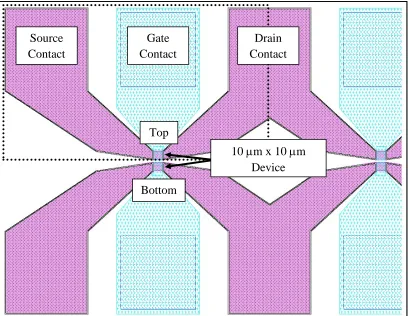
1.2.1. Architecture Modules D1, G3, J2
Three architectures were evaluated when conducting this study; they are
commonly referred to as D1, G3, and J2: all three have transistors containing 10 µm gate
widths. All three architectures have the same source/drain contact and gate contact layout
[image:27.612.121.529.340.656.2]as shown in Fig. 1.3.
Fig. 1.3: 10 µm x 10 µm (L x W) Ge PMOS source/drain contact and gate contact layout. This layout is the same for D1, G3, and J2 architectures.
Source Contact
Gate Contact
Drain Contact
10 µm x 10 µm Device Top
9
The device in the top of Fig. 1.3 is the same as the device in the bottom as noted. As one
moves device-to-device from left to right the gate length decreases: 10 µm; 5 µm; 1 µm;
0.8 µm; etc. Note in Figure 1.3 that the drain contact for this 10 µm x 10 µm (L x W) Ge
PMOS is also the source contact for the neighboring 5 µm x 10 µm (L x W) device. This
is important when considering the reverse bias source and drain leakages. The 10 µm
device has in essence one source and two drains, whereas the 5 µm; 1 µm; and 0.8 µm
devices have two sources and two drains, indicating possible optimization for MOSFET
leakage performance.
The differences between the three architectures are in their source/drain areas,
source/drain contact areas, and distance of source/drain metal contact to gate. The
differences are listed in Table 1.3. These differences played a significant role in the
trap-assisted leakages as observed in the devices. This will be discussed in Chapter 5.
Table 1.3: Difference between architectures D1, G3, and J2.
Arch S/D Area [µm2] S/DContact Area [µm2] S/DContact to Gate Distance [µm]
D1 2.20x10⁴ 2.10x10⁴ 1.5
G3 74 43 3.0
J2 74 43 1.5
1.3 Statement of Problem and Thesis Contribution
The investigation presented in this study started in an attempt to identify the
source(s) leading to an abnormal behavior in CGC when measuring the devices described
in Section 1.2. Specifically, this unknown behavior was observed as a parasitic
capacitance during CGC measurement dependent on both applied bias and frequency: this
10
minimizing the Ge-PMOS source/drain area and gate to source/drain-contact distance,
while maximizing both gate length and measurement frequency.
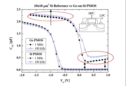
-2.0 -1.5 -1.0 -0.5 0.0 0.5 1.0 0.0
0.5 1.0 1.5 2.0 2.5
10x10 µµµµm2 Si Reference vs Ge-on-Si PMOS
1 MHz 100 kHz
C G
C
[
p
F
]
VG [V]
1 MHz 100 kHz
Ge PMOS
Si PMOS
HPC
[image:29.612.111.542.140.437.2]LPC
Fig. 1.4: Gate-to-Channel Capacitance (CGC) for two ~10 µm x 10 µm pMOSFETs. Plot reveals a large voltage and frequency-dependent parasitic capacitance in channel-accumulation for the Germanium PMOS resulting in a positive shift in CGC. This behavior is contrary to theory as shown by the Silicon PMOS. The source of this behavior was unknown prior to this study.
Fig. 1.4 shows the measurement of two PMOS technologies containing identical
TiN/TaN/HfO2/SiO2/Si gate stacks as outlined in Section 1.2. The Si-PMOS technology
behaves as predicted whereas the Ge-PMOS technology has a large voltage and
frequency-dependent parasitic capacitance resulting in a vertical shift of the CGC curve.
This raises concern in Ge-PMOS CGC values obtained in high channel-inversion, such as
those used to evaluate effective oxide thickness (EOT) and in Ge-PMOS CGC values
11
capacitance (COV). Prior to this study the parasitic capacitance was removed
mathematically at each frequency by subtracting the minimum parasitic capacitance
observed in accumulation at that frequency from the entire CGC curve of that frequency.
This provided questionable EOT results and no COV information (mathematical
subtraction results in a COV = 0.0 F) as observed in Chapter 6.
Initially, during C-V analysis reliable conductance information could not be
obtained. In all cases conductance was negative. To determine the Ge-PMOS leakage a
new DC measurement technique was created and called a MOS-Gated-Diode
measurement. The configuration of this measurement—designed to be similar to the CGC
configuration as shown in the inset of Fig. 1.4—shorts the Ge-PMOS source to the drain
and reverse biases them to the well, while sweeping the gate. This allowed leakage
mechanism evaluation and temperature-dependent analysis. It was found that leakage was
architecture-dependent: in terms of reverse bias leakage magnitude (IR): IR_D1>IR_G3>IR_J2.
Using the best device (J2 architecture 10 µm x 10 µm device), activation energy
extraction at each VG of the MOS-gated-diode measurement indicated which leakage
components were contributing throughout the CGC measurement. When analyzing the J2
architecture, results show that a significant amount of trap-assisted leakage (TAL) and
gate-induced-junction leakage (GIJL) existed at source/drain-to-well reverse biases as
low as 10 mV. Results also reinforced why conductance information had initially not
being obtained.
Obtaining reliable conductance information required the learning of two lessons:
counter-12
doped well technology and second, that grounding the substrate resulted in conductance
measurement error. The MOS-gated-diode measurement led the investigator to the cause
of the conductance measurement error. This study reveals that for obtaining reliable
conductance information the Ge-PMOS substrate must not be grounded during CGC
measurement. It was found that grounding the substrate during AC analysis induced a
compensation error in the C-V unit during measurement which remained—for at
minimum three re-compensations—thereafter. In extreme cases the capacitance would
shift to negative values.
This study links the trap-assisted and gate-induced-junction leakage mechanisms
observed during DC analysis to trap-assisted and gate-induced-junction conductance
observed during AC analysis. As a result the parasitic capacitance is broken into two
main components: a frequency-dependent source/well and drain/well trap-assisted
leakage (TAL) capacitance (CPara_SD) and a frequency-voltage dependent
gate-induced-junction leakage capacitance (CPara_GIJL). A third component due to channel depletion and
generation by traps is also identified (CIT). TAL was identified as a major leakage
component instead of Shockley-Read-Hall (SRH), because the activation energy
extracted during DC analysis was less than half the bandgap of Ge (bandgap of Ge is
0.66 eV).
Furthermore, the Conductance Method—first proposed by Nicollian and
Goetzberger in 1967 for use with capacitors but related to the CGC measurement of this
study—was used, revealing a Gaussian distribution in conductance versus frequency
attributed to trap-conductance. This trap-conductance is found to be geometry and
13
10 µm x 10 µm devices and become faster for smaller gate lengths throughout all
architectures. The trend in trap frequency response also corresponds to the DC leakage
evaluation performed.
1.4. Organization of Thesis
This thesis is broken down into seven chapters so as to better communicate the
study. Chapter 1 is an introduction and motivation section discussing why researchers are
interested in Germanium and III-V semiconducting technology and what this technology
actually entails. Chapter 2 describes the PMOS CGC measurement setup used in this
study, what equipment was used and why it was configured in the manner it was. This
chapter also discusses the parallel model assumption, the role of the high probes, the role
of the low probes, the CGC regions of operation, and ideal CGC behavior. The
experimental data in Chapter 2 is normalized so as to explain CGC and support the CGC
results presented in Chapter 3.
In Chapter 3 the CGC results are presented for the Ge PMOS devices described in
Section 1.2 of Chapter 1. The frequency dependence of CGC and conductance are
discussed. The capacitance and conductance of architectures D1, G3, and J2 are
measured for 10 µm; 5 µm; 1 µm gate lengths showing the parasitic capacitance behavior
as a function of both architecture and gate length. The Gaussian distribution of
conductance versus frequency reveals trap-assisted leakage behavior. Finally, the
parasitic capacitance is minimized using J2 architecture with 10 µm gate length. Chapter
4 discuses C-V tool compensation error due to measurement technique: grounding the Ge
14
Chapter 5 begins by discussing the typical leakage components—diffusion,
generation/trap-assisted, and gate-induced junction leakage—observed in reverse-biased
p/n junctions so as to discuss the MOS-Gated-Diode Measurement used in this study. In
Chapter 5 the source/drain to well leakage components are compared between
architecture modules and identified on the J2 Module through activation energy
extraction of the MOS-Gated-Diode measurement.
Chapter 6 extracts the extrinsic and intrinsic capacitances (CEXT) and (CGCO),
respectively. A new definition for CEXT is developed in considering the effect of CPara_SD ,
CPara_GIJL, and CIT. This definition relies on proper determination of VFB. From CGCO the
inversion capacitance is determined and the effective oxide thickness (EOT) extracted.
This EOT is compared to theoretical. The results do not match. The discrepancy is
explained through inversion layer quantization and compared to results published in
research. Finally, Chapter 7 is the conclusion of this work in which results are briefly
revisited along with a discussion of the future work needed to identify and further
15
References for Chapter 1
[1] R. M. Todi and M. M. Heyns. 2007. Germanium: The Semiconducting Comeback Material. IEEE Potentials: 34-38. http://ieeexplore.ieee.org/ (accessed March 17, 2008).
[2] International Technology Roadmap for Semiconductors. 2006. Process Integration, Devices, and Structures. 1-37. http://www.itrs.net/ (accessed August 15, 2008).
[3] B. De Jaeger, B. Kaczer, P. Zimmerman, K. Opsomer, G. Winderickx, J. Van Steenbergen, E. Van Moorhem, V. Terzieva, R. Bonzom, F. Leys, C. Arena, M. Bauer, C. Werkhoven, M. Caymax, M. Meuris, and M. Heyns. 2007. Ge Deep Sub-micron HiK/MG pFETs with Superior Drive Compared to Si HiK/MG State-of-the-art Reference. Semiconductor Science and Technology: 221-226.
http://www.sciencedirect.com (accessed March 12, 2008).
[4] R. Chau. 2006. Challenges and Opporunties of III-V Nanoelectronics for Future Logic Applications. Device Research Conference (DRC): 1-18.
“http://download.intel.com/technology/silicon/Chau_DRC_062606.pdf “ (accessed August 19, 2008).
[5] Intel. http://www.intel.com(accessed March 17, 2008).
[6] Advance Micro Devices, Inc. http://www.amd.com(accessed March 17, 2008).
[7] G. Nicholas, B. De Jaeger, D. P. Brunco, P. Zimmerman, G. Eneman, K. Martens, M. Meuris, and M. M. Heyns. 2007. High-Performance Deep Submicon Ge pMOSFETs With Halo Implants. IEEE Transactions on Electron Devices, vol. 54, no. 9: 2503-2511. http://ieeexplore.ieee.org/ (accessed March 17, 2008).
[8] U.S Geological Survey. http://minerals.usgs.gov/minerals/pubs/commodity/ (accessed November 5, 2008).
[9] P. Zimmerman, G. Nicholas, B. De Jaeger, B. Kaczer, A. Stesmans, L-A
Ragnarsson, D. P. Brunco, F. E. Leys, M. Caymax, G. Windericks, K. Opsomer, M. Meuris, and M. M. Heyns. 2006. High Performance Ge pMOS devices using a Si-compatible process flow. IEDM: 11-13. http://ieeexplore.ieee.org (accessed March 17, 2008).
[10] J.-S. Park, J. Bai, M. Curtin, B. Adekore, M. Carroll, and A. Lochtefeld. 2007. Defect reduction of selective Ge Epitaxy in trenches on Si(001) substrates using aspect ratio trapping. Applied Physics Letter, vol. 90, no. 052113: 1-3.
http://apl.aip.org/ (accessed August 15, 2008).
[11] J. Z. Li, J. Bai, J.-S. Park, B. Adekore, K. Fox, M. Carroll, and A. Lochtefeld. 2007. Defect reduction of GaAs epitaxy on Si (001) using selective aspect ratio trapping.
16
Chapter 2
PMOS Gate-to-Channel Capacitance (C
GC)
Equipment/Measurement
The goal of this chapter is to describe the C-V equipment configuration used in
this study, the C-V measurement setup used in this study, and the ideal behavior of
PMOS Gate-to-Channel Capacitance (CGC) so as to provide background for the deviation
in Ge-PMOS CGC behavior observed and discussed in the next chapter. During this study
three equipment configurations were briefly evaluated as shown in Table 2.1.
Configuration-3 was found to be the best due to both its open compensation (correcting
for stray admittance due to the test fixture) and short compensation (correcting for stray
impedance due to the test fixture) capabilities [1]. The Keithley K4200 in
Configuration-1 and Configuration-2 allowed for open compensation only. As a result, all CGC
measurements presented in this study were performed using Configuration-3.
Table 2.1: The three equipment configurations available to measure CGC.
Configuration Probe Station C-V Meter C-V Control and Data
Acquisition 1 Cascade Microtech
Manual Microchamber
Agilent 4284A 20 hz-1 MHz Precision LCR (Agilent 4284A)
Keithley K4200 through General Purpose Interface Bus
(GPIB) 2 SUSS MicroTec
PA300PS
Agilent 4284A Keithley K4200 through GPIB 3 SUSS MicroTec
PA300PS
17
Besides the compensation capabilities of Configuration-3 in Table 2.1, it was
found that the lack of a switching matrix—utilized in both Keithley setups—provided a
system with less Unknown Terminal to DUT separation. This meant less cable length
resulting in better cable calibration. Lastly, the Keithley CGC measurement program of
Configuration-1 and Configuration-2 grounded the Ge-PMOS substrate resulting in C-V
Meter compensation error. This will be described in more detail in Chapter 4.
Configuration-3 did not ground the Ge-PMOS substrate. As a result, Configuration-3 will
be the only configuration discussed in this chapter.
2.1. C-V Equipment and Configuration
The Suss MicroTec PA300PS probe station used in Configuration-3 of this study
and shown in Fig. 2.1 is a semi-automatic device characterization tool [2]. Consisting of a
Semiautomatic Wafer Controller, iVista Microscope, Probe Shield Technology, and
PH110 SUSS Microtec Micromanipulators, this station is capable of accurately analyzing
devices located on single chips or on wafers as large as 300 mm in diameter.
The Semiautomatic Wafer Controller of the PA300PS allows for both easy
movement die-to-die and probe lift/drop during measurement (provided the height and
location of the probe tips inside the probe shield housing are set correctly to minimize
contact scratching). This allows one to map the die performance of an entire wafer. The
iVista Microscope allows one to zoom in on the contacts vertically and view them
laterally thereby ensuring connection between the probe tip and device contact. The
Probe Shield Technology provides an environment free from both electromagnetic
requirement from an expensive EMI/RFI shielded room. Shielding is extremely important
[image:37.612.159.489.141.446.2]when performing precise noise
Fig. 2.1: A SUSS Microtec.
Aside from the features above, the Probe Station floats on hydraulic feet, thereby
protecting the wafer and probe tips from minor vibrations, such as in those caused by the
slamming of a door, making it perfect for time
heater and chiller are attached to the station, allowing temperature
measurements. Finally, the wafer handling system is designed for wafer fragility [2]
making it perfect for Germanium and III
Semi-auto Controller
iVista Microscope
Probe Shield Technology
18
requirement from an expensive EMI/RFI shielded room. Shielding is extremely important
when performing precise noise-free C-V analysis.
A SUSS Microtec. semiautomatic probe station PA300PS adopted from [2].
Aside from the features above, the Probe Station floats on hydraulic feet, thereby
protecting the wafer and probe tips from minor vibrations, such as in those caused by the
slamming of a door, making it perfect for time-dependent electrical analysis. A chu
heater and chiller are attached to the station, allowing temperature
measurements. Finally, the wafer handling system is designed for wafer fragility [2]
making it perfect for Germanium and III-V devices.
Wafer Entry uto Controller
iVista Microscope
Image Reproduced with Permission Courtesy of SUSS
Microtec.
requirement from an expensive EMI/RFI shielded room. Shielding is extremely important
semiautomatic probe station PA300PS adopted from [2].
Aside from the features above, the Probe Station floats on hydraulic feet, thereby
protecting the wafer and probe tips from minor vibrations, such as in those caused by the
dependent electrical analysis. A chuck
heater and chiller are attached to the station, allowing temperature-dependent
measurements. Finally, the wafer handling system is designed for wafer fragility [2]
Entry
Image Reproduced with Permission, Courtesy of SUSS
The C-V Meter used in this study cons
Precision LCR Meter—
[image:38.612.110.543.169.526.2]through a General Purpose Interface Bus (GPIB).
Fig. 2.2: Front Panel of the
from [3] showing location of the Unknown Terminals and their connection/configuration with the Connector Plate through the Coax Cable Extensions. The total cable length (1) is composed of the triax cable extensions (2), in connection with the coax cable extensions (3) and the probe tips (4). The cable lengths are not to scale. The cable length between (2 3) is exaggerated here for illustration only.
The configuration of the HP
perhaps the most important aspect of the
measurement accuracy at low and high frequ
© Agilent Technologies, Inc. 2001. Reproduced and Modified
with Permission, Courtesy of Agilent Technologies, Inc.
19
Meter used in this study consists of an Agilent 4284A 20Hz
—shown in Fig. 2.2—controlled by a Unix Computer System
through a General Purpose Interface Bus (GPIB).
Front Panel of the Agilent 4284A 20 Hz – 1 MHz Precision LCR Meter adapted from [3] showing location of the Unknown Terminals and their connection/configuration Plate through the Coax Cable Extensions. The total cable length (1) is composed of the triax cable extensions (2), in connection with the coax cable extensions (3) and the probe tips (4). The cable lengths are not to scale. The cable length between (2
s exaggerated here for illustration only.
The configuration of the HP-4284A Unknown Terminals with respect to the probe tips is
perhaps the most important aspect of the C-V equipment configuration when considering
measurement accuracy at low and high frequencies. This is due to the need for software
(1)
(2) (3) (4)
Agilent 4284A 20Hz-1MHz
controlled by a Unix Computer System
MHz Precision LCR Meter adapted from [3] showing location of the Unknown Terminals and their connection/configuration Plate through the Coax Cable Extensions. The total cable length (1) is composed of the triax cable extensions (2), in connection with the coax cable extensions (3) and the probe tips (4). The cable lengths are not to scale. The cable length between
(2-4284A Unknown Terminals with respect to the probe tips is
equipment configuration when considering
encies. This is due to the need for software
20
calibration of cable length and compensation of stray admittances and impedances due to
the testing fixture.
In general the following conditions are sought and labeled in Fig. 2.2
appropriately. The signal path between the 4284A and the probe tips (1) should be as
short as possible; High Current (HCUR), High Potential (HPOT), Low Potential (LPOT), and
Low Current (LCUR) coax extension cables (2) should be as short as possible and they
should be connected as close as possible to the DUT (3+4); the distance between the
DUT and the shields of the coax extension cables (4) should be as short as possible [3].
Following these four conditions minimizes the cable length calibration required. This
minimizes stray capacitive, inductive, and resistive components existing between the
Unknown Terminals and the probe tips thereby allowing for more accurate open/short
compensation. By obtaining better parasitic admittance/impedance compensation, one
may obtain an effective capacitance value as close as possible to the true theoretical value
of the DUT.
The terminal configuration shown in Fig. 2.2 is close to one known as a
5-Terminal Pair Configuration used in typical frequency measurement ranges of 10 mHz –
100 MHz [1], but different in the fact that, first, it contains two Low Probe Contacts
(labeled S and D) and, secondly, it does not contain shield shorting at the end of the coax
cables near the DUT (4). Shield shorting at the end of the coax cables near the DUT was
not performed in any measurements conducted within the scope of this study due to the
21
2.2. Measurement Setup of Capacitance and Conductance
To understand how capacitance and conductance are extracted from the DUT, it is
important to understand the role of impedance. Impedance (Z) is defined as the
measurement of the total opposition of a device or circuit to AC current flow [1]. When
measured it exists as a complex quantity containing both real and imaginary quantities
known as resistance (R) and reactance (X), respectively. Reactance (X) can take on an
inductive or a capacitive form as shown in Eq. 2.1 and Eq. 2.2, respectively where ω is
the angular frequency of the applied signal, Lmat is the material inductance, and Cmat is the
material capacitance.
2 (2.1)
(2.2)
If resistance and reactance are in series with one another the impedance is
measured as the mathematical sum of the two. This is shown as inset (a) of Fig. 2.3.
Fig. 2.3: Impedance (Z) and admittance (Y) representations adopted from [1]. (a)
Impedance series configuration of resistance (R) and reactance (X). (b) Impedance parallel configuration transformed into a simpler expression known as admittance (Y). Admittance is composed conductance (G) and susceptance (B).
(a)
(b)
Real and imaginary components in series
Real and imaginary components in parallel
© Agilent Technologies, Inc. 2001. Reproduced and Modified with Permission,
22
If, on the other hand, these quantities are in parallel to one another—as in the case of
gate-to-channel capacitance evaluated in this study—impedance is measured as shown in
the top of inset (b) of Fig. 2.3. In this case it is often much more convenient
mathematically to consider Admittance (Y) as shown in bottom of this inset.
Admittance, as is shown in the bottom of inset (b) of Fig. 2.3 and in Eq. 2.3, is the
inverse of impedance and is measured in Siemens. Admittance is also a complex
quantity, composed of both real and imaginary quantities known as conductance (G) and
susceptance (B), respectively.
(2.3)
There are several methods available to measure the impedance or admittance of a
DUT. Such include the Bridge, Resonant, I-V, RF I-V, Network Analysis, and Auto
Balancing Bridge methods. Reference is made to the Agilent Technologies Impedance
Measurement Handbook [1] for specific details on each of these methods. All have their
advantages and disadvantages. The Agilent 4284A used in this study uses the
Auto-Balancing Bridge Method.
2.2.1. Auto-Balancing Bridge Method
The Agilent 4284A uses an Auto-Balancing Bridge Method to measure
impedance of the DUT. The advantage of this method is that, first, it has wide frequency
coverage (20 Hz – 110 MHz provided the C-V meter supports it); second, it has high
accuracy over a wide impedance measurement range provided the equipment
23
main disadvantages are 1.) frequency ranges higher than 110 MHz cannot be measured
and 2.) grounded DUT measurements—though possible by grounding the DUT as shown
in Fig. 2.4—are difficult to perform because the measurement signal current can bypass
the Low Probe amplifier network shown in Fig. 2.4, which can provide erroneous
[image:42.612.117.534.219.443.2]capacitance and conductance values [1].
Fig. 2.4: Auto-Balancing Bridge Method impedance measurement adapted from [1]. The
potential at the High Probes (HPC) varies through time as it is the input signal (DC sweep with AC signal superimposed). The potential at the Low Probes (LPC) is maintained at zero volts: it is called “virtual ground” for current passing through R is balanced with the current passing through the DUT using the I-V converter amplifier [1]. The impedance is calculated using the voltage at the HPC terminal and the current which crosses the resisting network R [1].
The most important aspect of the Auto-Balancing Bridge method is the fact that
the measured impedances—in the case of this study translated to admittance—are only as
accurate in value and behavior as the assumptions made about the DUT. In the case of the
Auto-Balancing Bridge, it is assumed when using the parallel model—where the
conductance and susceptance are parallel to each other resulting in the admittance
representation—that, first, little current flows from the High Probes through the DUT to
V
V
OSC
R
HPC
LPC
DUT
Z
© Agilent Technologies, Inc. 2001. Reproduced
24
the Low Probes and, second, that any current flowing into or out of the Low Probe is a
result of DUT leakage from the high probe. The first case was found to be true in this
study for DC analysis revealed gate leakage in the 1x10-11 A to 1x10-12 A range. The
second case was found not to be true and affected the measured impedance which
translated into non-ideal capacitance and non-ideal conductance behavior.
2.3. Purpose of CGC, Regions of Operation, and Ideal Behavior
In order to compare new germanium MOSFET technologies with existing silicon
MOSFET technology basic electrical analysis is required. This section will discuss a
measurement known as Gate-to-Channel Capacitance (CGC), in common use during both
gate stack characterization and the benchmarking of advanced devices. During gate stack
characterization, parameters such as Effective Oxide Thickness (EOT), channel threshold
voltage (VT), and Interface Trap Density (Dit) [4, 5] are commonly sought. During the
benchmarking of advanced devices, parameters such as External Capacitance (CEXT),
Effective Channel Length (LEFF), Inversion Charge (Qi), Effective Carrier Mobility (µeff),
and Saturation Velocity (νsat) [5-9] are commonly sought.
Due to the wide use of CGC as a foundation for Ge MOSFET characterization—
µeff and νsat require MOSFET IDS versus VGS analysis [7,8], also referred to as Split C-V
Analysis—CGC accuracy is an extremely important issue. This is especially true at
smaller channel lengths where the drain and source regions become a significant
contributor to CGC [6]. During this study the investigator observed that Ge MOSFET CGC
did not always obey the known behaviors as expected from literature [10], research [4-9,
25
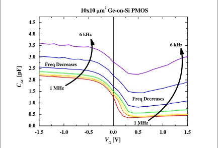
In particular, the Ge CGC observed during channel accumulation was
frequency-dependent and larger than expected (in the pF range versus the fF range) [12] resulting in
a vertical shift in the CGC curve as seen in inversion [12]. The exact reason for this was
unknown until this study and will be discussed in Chapter 3. To better understand the CGC
measurement let us look at its configuration with a PMOSFET.
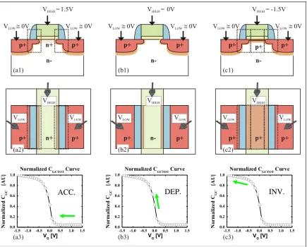
2.3.1. Connection to Generic PMOSFET
In this study CGC was measured by connecting the High Probe Contact (HPC) and
the two Low Probe Contacts (LPCs) – initially shown in Fig. 2.2 – to the MOSFET DUT
as follows: the HPC is connected to the Gate, one of the LPCs is connected to the Source
and the other LPC to the Drain. This CGC connection scheme is shown in the (a1; b1; c1;
a2; b2; c2) insets of Fig. 2.5. The LPCs are kept at virtual ground, meaning that the C-V
meter senses the LPCs and biases them appropriately to maintain a 0 V bias on the
Source and Drain. The HPC is swept from accumulation to inversion and vice versa
while superimposing an AC voltage signal throughout the biasing range. This AC voltage
signal is used to determine the admittance in the parallel model—composed of a
26
Fig. 2.5: Standard CGC connection and measurement for PMOS. Horizontal (a1, b1, c1) and vertical (a2, b2, c2) illustrations of HPC (VHIGH) and LPCs (VLOW) connections.
Normalized CGC Curve (a3, b3, c3) illustrate modes of operation. There are three general
CGC modes: that at accumulation, depletion, and inversion.
The result of this CGC connection as measured at accumulation, depletion, and
inversion of a Si-PMOS is shown in Fig. 2.5. Notice that the CGC capacitance is
normalized to the maximum capacitance as observed in high inversion so as to illustrate
the regions of MOSFET operation. In accumulation the capacitance measured between
the HPC and LPC is illustrated in insets (a1, a2) and shown in inset (a3) of Fig. 2.5. It is
observed that in accumulation the capacitance is extremely small. During depletion
(b1-b3) the capacitance increases. It is here that the CIT contributes. As the gate is swept to
inversion as illustrated in insets (c1, c2), the capacitance becomes very large. The
capacitance in accumulation is typically referred to as the extrinsic capacitance, for most
of it resides near the peripheries of the MOS channel; whereas that in inversion is
typically referred to as the intrinsic capacitanc
2.3.2. High Accumulation and High Inversion
Fig. 2.6 can help explain why the accumulation capacitance is very small when
compared to the inversion capacitance. Fig. 2.6 illustrates the extrinsic capacitance
observed in channel accumulation and the intrinsic capacitance observed in channel
inversion. The gate-to-channel capacitance measured in high inversion is the sum of the
extrinsic and intrinsic capacitances in parallel.
Fig. 2.6: Components of high accu
components of accumulation capacitance and (b) the component of as adapted from [10].
Referring to inset (a) of Fig. 2.6, it can be inferred that during accumulation there
exists no inversion channel. As a result, in accumulation only the capacitances between
HPC and LPCs are observed. These result from gate overlap with the source/drain (
inner fringing fields between the gate and source/drain (
27
capacitance in accumulation is typically referred to as the extrinsic capacitance, for most
of it resides near the peripheries of the MOS channel; whereas that in inversion is
typically referred to as the intrinsic capacitance, for it resides within the MOS channel.
High Accumulation and High Inversion
Fig. 2.6 can help explain why the accumulation capacitance is very small when
compared to the inversion capacitance. Fig. 2.6 illustrates the extrinsic capacitance
bserved in channel accumulation and the intrinsic capacitance observed in channel
channel capacitance measured in high inversion is the sum of the
extrinsic and intrinsic capacitances in parallel.
Components of high accumulation and high inversion capacitance
components of accumulation capacitance and (b) the component of inversion capacitance
Referring to inset (a) of Fig. 2.6, it can be inferred that during accumulation there
no inversion channel. As a result, in accumulation only the capacitances between
HPC and LPCs are observed. These result from gate overlap with the source/drain (
inner fringing fields between the gate and source/drain (CIF), outer fringing fields capacitance in accumulation is typically referred to as the extrinsic capacitance, for most
of it resides near the peripheries of the MOS channel; whereas that in inversion is
e, for it resides within the MOS channel.
Fig. 2.6 can help explain why the accumulation capacitance is very small when
compared to the inversion capacitance. Fig. 2.6 illustrates the extrinsic capacitance
bserved in channel accumulation and the intrinsic capacitance observed in channel
channel capacitance measured in high inversion is the sum of the
mulation and high inversion capacitance. (a) The four inversion capacitance
Referring to inset (a) of Fig. 2.6, it can be inferred that during accumulation there
no inversion channel. As a result, in accumulation only the capacitances between
HPC and LPCs are observed. These result from gate overlap with the source/drain (COV),
28
between the gate and source/drain (COF), and top capacitance as seen through the
insulator between gate and source/drain contact (CTOP). Likewise, inset (b) of Fig. 2.6
shows that during ideal inversion there exists an inverted channel below the gate
connecting source to drain. From this connection an additional capacitance between the
HPC and LPCs, known as the inversion capacitance (CGCO), is observed. Assuming the
inversion layer is at the channel surface, this inversion channel capacitance is considered
a parallel plate capacitance proportional to the gate area and dielectric constant and
inversely proportional to the dielectric thickness. This gate-to-channel capacitance (CGC)
is the sum of the extrinsic and intrinsic capacitance in parallel.
The ideal CGC—as shown in Eq. 2.4—is the mathematical sum of the ideal
extrinsic capacitance (CEXT), the ideal inversion capacitance (CGCO), and the ideal
parasitic capacitance (CPara).
CV, f#|%&'()_+', C-V# C./0V# C1232V, f# (2.4)
The extrinsic capacitance in Eq. 2.5 is twice the CIF that is gate-bias dependent—
meaning that it is decoupled during inversion—and twice the outer capacitance (CO) that
is geometry and material dependent as shown in Eq. 2.6.
C./0V# 2C4%V# 2C- (2.5)
C- C0-1 C-% C-5 (2.6)
Due to line calibration and open/short compensation error, a small CPara may exist
29
frequency and voltage-dependent. It is common to mathematically subtract CPara from
CGC after measurement. By subtracting CPara from the CGC curve it is quite obvious that
one removes the COV information while maintaining the CGCO information. Minimizing
CPara prior to measurement allows one to approach the effective total capacitance, which
provides a near true CGCO and COV.
![Fig. 1.1: Intel’s 2006 device trend-projection adopted from Chau [4]. Note that Intel’s research projection is more aggressive than that of the ITRS](https://thumb-us.123doks.com/thumbv2/123dok_us/56985.5280/21.612.118.531.204.461/intel-device-projection-adopted-intel-research-projection-aggressive.webp)
![Fig. 1.2: Ge PMOSFET adopted from [7]. Note that backend metallization has been omitted](https://thumb-us.123doks.com/thumbv2/123dok_us/56985.5280/26.612.140.509.421.648/fig-ge-pmosfet-adopted-note-backend-metallization-omitted.webp)
![Fig. 2.1: A SUSS Microtec. A SUSS Microtec. semiautomatic probe station PA300PS adopted from [2]](https://thumb-us.123doks.com/thumbv2/123dok_us/56985.5280/37.612.159.489.141.446/suss-microtec-suss-microtec-semiautomatic-probe-station-adopted.webp)
![Fig. 2.2: Front Panel of the from [3] showing location of the Unknown Terminals and their connection/configuration with the Connector Plate through the Coax Cable Extensions](https://thumb-us.123doks.com/thumbv2/123dok_us/56985.5280/38.612.110.543.169.526/showing-location-unknown-terminals-connection-configuration-connector-extensions.webp)
![Fig. 2.4: Auto-Balancing Bridge Method impedance measurement adapted from [1]. The potential at the High Probes (HPC) varies through time as it is the input signal (DC sweep with AC signal superimposed)](https://thumb-us.123doks.com/thumbv2/123dok_us/56985.5280/42.612.117.534.219.443/balancing-bridge-method-impedance-measurement-adapted-potential-superimposed.webp)