N A N O E X P R E S S
Open Access
Influence of the ratio of gate length to
drain-to-source distance on the electron mobility in
AlGaN/AlN/GaN heterostructure field-effect
transistors
Yuanjie Lv
1, Zhaojun Lin
1*, Lingguo Meng
1, Chongbiao Luan
1, Zhifang Cao
1, Yingxia Yu
1, Zhihong Feng
2and Zhanguo Wang
3Abstract
Using measured capacitance-voltage curves with different gate lengths and current–voltage characteristics at low source voltage for the AlGaN/AlN/GaN heterostructure field-effect transistors (HFETs) of different drain-to-source distances, we found that the dominant scattering mechanism in AlGaN/AlN/GaN HFETs is determined by the ratio of gate length to drain-to-source distance. For devices with small ratio (here, less than 1/2), polarization Coulomb field scattering dominates electron mobility. However, for devices with large ratio (here, more than 1/2), longitudinal optical (LO) phonon scattering and interface roughness scattering are dominant. The reason is closely related to polarization Coulomb field scattering.
Keywords:electron mobility, drain-to-source distance, AlGaN/GaN heterostructures, polarization Coulomb field scattering
Background
Owing to potential applications in high power and high frequency electronic devices associated with outstanding material properties, AlGaN/GaN heterostructure field effect transistors (HFETs) have attracted extensive re-search to improve the device performance [1-3]. The strained AlGaN/AlN/GaN heterostructure with a thin AlN interlayer has been the popular material structure for AlGaN/GaN HFETs due to the improved transport properties of two-dimensional electron gas (2DEG) and electron mobility [4,5]. According to our former report, it is found that the ratio of gate length to drain-to-source distance has an important influence on electron mobility and determines the dominant scattering mech-anism in the AlGaN/AlN/GaN HFETs with the drain-to-source distance of 100μm [6]. However, the above influ-ence on the electron mobility in AlGaN/AlN/GaN HFETs with different drain-to-source distances has not been investigated. Meanwhile, mainstream microwave
power AlGaN/AlN/GaN HFETs are in small-size drain-to-source distances [7]. Therefore, it is of great import-ance to investigate the influence of the ratio of gate length to drain-to-source distance on the electron mo-bility in AlGaN/AlN/GaN HFETs with different drain-to-source distances. In this study, rectangular AlGaN/ AlN/GaN HFETs with different drain-to-source dis-tances and gate geometrical areas were fabricated, and the influence of the ratio of gate length to drain-to-source distance on the electron mobility in AlGaN/AlN/ GaN HFETs with different drain-to-source distances was investigated.
Methods
The heterostructure layer employed in this study was grown by molecular beam epitaxy on a (0001) sapphire substrate. The structure consists of a 40-nm AlN nucle-ation layer, followed by a 3-μm undoped GaN layer, a 0.5-nm AlN interlayer, and a 22.5-nm-thick undoped Al0.28Ga0.72N layer. Hall measurements indicated a sheet carrier density of around 1.1 × 1013 cm−2 and an electron mobility of 1,800 cm2/Vs at room temperature.
* Correspondence:[email protected]
1School of Physics, Shandong University, Jinan 250100, China
Full list of author information is available at the end of the article
For device processing, mesa isolation was performed using Cl2/BCl3 reactive ion etching. The source and drain ohmic contacts were formed by depositing Ti/Al/ Ni/Au using e-beam evaporation and lift-off and then were annealed in a rapid thermal annealing system. With transmission line method patterns, the specific resistivity of the contacts was measured to be 7 × 10⁻⁵Ωcm2. The source and drain contacts were rectangular: 100 μm wide and 50μm long. Drain-to-source distances with 60, 20, 15, and 9 μm were prepared. Ni/Au (60/160 nm) Schottky contacts of varying areas were then deposited symmetrically in the middle between the source and drain ohmic contacts by e-beam evaporation. The Schottky contact sizes in AlGaN/AlN/GaN HFETs with a 60-μm drain-to-source distance are 12/100 (length/
width), 24/100, 36/100, and 48/100 μm which are
marked as 60-a, 60-b, 60-c, 60-d, respectively. The Schottky contact sizes in AlGaN/AlN/GaN HFETs with a 20-μm drain-to-source distance are 4/100 (length/ width), 8/100, 12/100, and 16/100μm which are marked as 20-a, 20-b, 20-c, 20-d, respectively. Schottky contacts of 3/100 μm (length/width) were deposited in AlGaN/ AlN/GaN HFETs with 15- and 9-μm drain-to-source distances which are marked as 15-a and 9-a, respectively. Capacitance-voltage (C-V) measurements were per-formed at room temperature using an Agilent B1520A (Agilent Technologies, Inc., Santa Clara, CA, USA) at 1 MHz, and current–voltage (I-V) measurements for the AlGaN/AlN/GaN HFETs were also performed at room
temperature using an Agilent B1500A semiconductor parameter analyzer.
Results and discussion
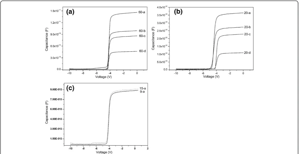
Figure 1 shows the C-Vcurves of the Ni Schottky con-tacts with different areas for the devices with drain-to-source distances of 60, 20, 15, and 9 μm, respectively. The C-Vmeasurements were obtained using the source contact and the Ni Schottky contact. The different threshold voltages of samples 20-c and 20-d with respect to samples 20-a and 20-b were due to the different strains under the Schottky contacts caused by the differ-ent Schottky contact areas [8]. The 2DEG electron dens-ity (n2D) under different gate biases with different Ni Schottky contact areas can be obtained by the integra-tion of the measured C-Vcurves [9], and the calculated results are shown in Figure 2.
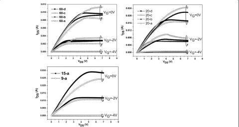
[image:2.595.56.540.454.703.2]The I-V characteristics for the rectangular AlGaN/ AlN/GaN HFETs with different drain-to-source dis-tances were measured and shown in Figure 3. The satur-ation current is higher with shorter gate length due to the long distance between the drain and gate edge. The abnormality of 60-d and 20-d may be due to the nonuni-formity of the AlGaN/GaN heterostructures or the ohmic contacts. The electron mobility of the 2DEG in the strained AlGaN/AlN/GaN heterostructures can be calculated with the I-V characteristics and 2DEG elec-tron density as described in [6]. Due to the low specific resistivity of the ohmic contacts (7 × 10⁻⁵Ωcm2), the
source and drain resistances were ignored during the calculation. The calculated results are shown in Figure 4. Also, the 2DEG electron mobility of the rectangular
AlGaN/AlN/GaN HFETs with drain-to-source of
100μm in [6] was also shown in Figure 4a, and from the
smallest to the largest in Schottky contact sizes, they are marked as 100-a, 100-b, 100-c, and 100-d.
[image:3.595.58.538.89.330.2]As one can see from Figure 4, the 2DEG electron mo-bility increases with gate voltage for the devices with small ratio of gate length to drain-to-source distance Figure 2Calculated 2DEG electron densityn2Dunder different gate biases.They are for samples with drain-to-source distances of 60 (a), 20
(b), and 15 and 9μm (c).
[image:3.595.58.539.448.704.2](here, less than 1/2),but it decreases for the one with large ratio (here, more than 1/2). It is well known that there are mainly five kinds of important scattering mechanisms to affect the 2DEG electron drift mobility in AlGaN/GaN HFET samples, and these scattering mechanisms are ionized impurity scattering [9], disloca-tion scattering [10], polarizadisloca-tion Coulomb field scatter-ing [6,9], longitudinal optical (LO) phonon scatterscatter-ing, and interface roughness scattering [11]. The ionized im-purity scattering and dislocation scattering can be ignored in our samples as discussed in [6]. The variety of electron mobility according to the gate bias can be explained as follows.
The Schottky gate produced a partial strain relaxation in the AlGaN layer, and then the polarization charges at AlGaN/AlN interface are distributed irregularly (spatial correlation is only partial) [8]. Thus, an additional scat-tering potential (polarization Coulomb field scatscat-tering potential) in comparison with the un-gated heterostruc-ture is formed. For polarization Coulomb field scatter-ing, the electron mobility rises with the increasing
[image:4.595.57.540.90.439.2]the dominant scattering mechanism in the AlGaN/AlN/ GaN HFETs is determined by the ratio of gate length to drain-to-source distance. With the ratio of less than 1/2, the polarization Coulomb field scattering dominates the 2DEG electron mobility in the AlGaN/AlN/GaN HFETs, while with the ratio larger than 1/2, the LO phonon scattering and the interface roughness scattering are dominant in the devices.
Conclusions
In summary, Ni Schottky contacts of different geomet-rical areas were deposited on strained AlGaN/AlN/GaN heterostructures with different drain-to-source distances. With the measured C-Vcurves and the I-V characteris-tics of AlGaN/AlN/GaN HFETs, we have investigated the influence of the ratio of gate length to drain-to-source distances on the electron mobility of the 2DEG in rectangular AlGaN/AlN/GaN HFET devices. We found that the dominant scattering mechanism in the AlGaN/AlN/GaN HFETs is determined by the ratio of gate length to drain-to-source distance. For the devices with small ratio (here, less than 1/2), the polarization Coulomb field scattering dominates the 2DEG electron mobility. For the devices with large ratio (here, more than 1/2), the LO phonon scattering and the interface roughness scattering are dominant.
Competing interests
The authors declare that they have no competing interests.
Acknowledgments
This work was supported by the National Natural Science Foundation of China (grant nos. 10774090 and 11174182), the National Basic Research Program of China (grant no. 2007CB936602), and the Specialized Research Fund for the Doctoral Program of Higher Education (grant no.
20110131110005).
Author details
1School of Physics, Shandong University, Jinan 250100, China.2Science and
Technology on ASIC Laboratory, Hebei Semiconductor Research Institute, Shijiazhuang 050051, China.3Laboratory of Semiconductor Materials Science,
Institute of Semiconductors, Chinese Academy of Sciences, Beijing 100083, China.
Authors’contributions
YL designed this study and drafted the manuscript. ZL instructed this study and revised the manuscript. LM and CL performed the sample preparation. ZC and YY carried out the experimental measurements. ZF and ZW participated in the critical discussions. All authors read and approved the final manuscript.
Received: 6 June 2012 Accepted: 14 July 2012 Published: 3 August 2012
References
1. Ambacher O, Foutz B, Smart J, Shealy JR, Weimann NG, Chu K, Murphy M, Sierakowski AJ, Schaff WJ, Eastman LF, Dimitrov R, Mitchell A, Stutzmann M:
Two dimensional electron gases induced by spontaneous and piezoelectric polarization in undoped and doped AlGaN/GaN heterostructures.J Appl Phys2000,87:334–344.
2. Gonschorek M, Carlin JF, Feltin E, Py MA, Grandjean N, Darakchieva V, Monemar B, Lorenz M, Ramm G:Two-dimensional electron gas density in
Al1−xInxN/AlN/GaN heterostructures (0.03≤x≤0.23).J Appl Phys2008,
103:093714.
3. Mizutani T, Ito M, Kishimoto S, Nakamura F:AlGaN/GaN HEMTs with thin InGaN cap layer for normally off operation.IEEE Electron Device Lett2007,
28:549–551.
4. Shen L, Heikman S, Moran B, Coffie R, Zhang NQ, Buttari D, Smorchkova IP, Keller S, DenBaars SP, Mishra UK:AlGaN/AlN/GaN high-power microwave HEMT.IEEE Electron Device Lett2001,22:457–459.
5. Lee JS, Kim JW, Lee JH, Kim CS, Oh JE, Shin MW, Lee JH:Reduction of current collapse in AIGaN/GaN HFETs using AIN interfacial layer.Electron Lett2003,39:750–752.
6. Lv YJ, Lin ZJ, Zhang Y, Meng LM, Luan CB, Cao ZF, Chen H, Wang ZG:
Polarization Coulomb field scattering in AlGaN/AlN/GaN heterostructure field-effect transistors.Appl Phys Lett2011,98:123512.
7. Chung JW, Hoke WE, Chumbes EM, Palacios T:AlGaN/GaN HEMT with 300-GHz fmax.IEEE Electron Device Lett2010,31:195–197.
8. Lin ZJ, Zhao JZ, Corrigan TD, Wang Z, You ZD, Wang ZG, Lu W:The influence of Schottky contact metals on the strain of AlGaN barrier layers.J Appl Phys2008,103:044503.
9. Zhao JZ, Lin ZJ, Corrigan TD, Wang Z, You ZD, Wang ZG:Electron mobility related to scattering caused by the strain variation of AlGaN barrier layer in strained AlGaN/GaN heterostructures.Appl Phys Lett2007,91:173507. 10. Jena D, Gossard AC, Mishra UK:Dislocation scattering in a
two-dimensional electron gas.Appl Phys Lett2000,76:1707–1709. 11. Ridley BK, Foutz BE, Eastman LF:Mobility of electrons in bulk GaN and
AlxGa1−xN/GaN heterostructures.Phys Rev B2000,61:16862–16869.
doi:10.1186/1556-276X-7-434
Cite this article as:Lvet al.:Influence of the ratio of gate length to drain-to-source distance on the electron mobility in AlGaN/AlN/GaN heterostructure field-effect transistors.Nanoscale Research Letters2012
7:434.
Submit your manuscript to a
journal and benefi t from:
7 Convenient online submission
7 Rigorous peer review
7 Immediate publication on acceptance
7 Open access: articles freely available online
7 High visibility within the fi eld
7 Retaining the copyright to your article