THE AES - 80
MICROPROCESSOR
:
I
:
:
MICROPROCESSOR
REFERENCE
MANUAL
PROPRIETARY NOTICE: This publication contains proprietary information of Automatic Electronic Systems Inc. and shall not be reproduced, copied, or used for any purpose other than the consideration of technical content without the express written permission of a duly authorized represen-tative of Automatic Electronic Systems Inc.
AUTOMATIC ELECTRONIC SYSTEMS INC., 5455 Pare Street
I .
II.
AES MICROPROCESSOR
TABLE OF CONTENTS
System Design Features
Page 1 1.~ 1.1 1.2 1.3 1.4 1.5 1.6 1.7 1.8 1.9 1.1~
General Characteristics Physical Configuration System Organization Instruction Memory Data Memory
Arithmetic Logic Unit Registers
1.6.~ P-Register 1.6.1 A-Register 1.6.2 L-Register 1.6.3 LA-Register 1.6.4 B-Register 1.6.5 U-Register Decision Flags Push Do\vn Stack
Instruction Timing Input/Output Interface
1 1 2 2 3 4 4 4 4 4 5 5 5 5 6 6 6
Microinstruction Repertoire 1~
2.~ 2.1 2.2 2.3 2.4 2.5 2.6 2.7 2.8 2.9 2.1~ 2.11 2.12 2.13 2.14 2.15
Instruction Formats 1~
2.~.~ Function 1~
2.~.1 Decision l~
2.~.2 ROM Address 11
2.~.3 RAM Address 11
2.~.4 Data Literal 11
2.~.5 ALU Literal 12
III.
IV.
V.
VI.
Input/Output
3 .~
3.1 3.2 3.3 3.4
Timing
4.
JJ
4.1 4.2 4.3serial I/O
3.~.1 I/O Bus Structure
3.~.2 Modular System Unit Bus Interface
3.~.3 Typical I/O Board
3.~.4 Serial I/O Interrupt Interrupt Structure
Parallel I/O
Multiprocessor Configuration I/O Instructions
3~4.l U-Register Instructions
3.4.2 I/O Register Select Instructions 3.4.3 I/O Channel Select Instruction 3.4.4 Serial I/O Clock, Load and R/W
3.4.5 3.4.6 3.4 .. 7 3.4.8
Instructions
Relinquish Bus Control Instructions Serial I/O Timing Instructions
Interrupt Instructions Other I/O Instructions
Function and Literal Timing Branch Instruction Timing Subroutine Timing
I/O Timing
Program Development and Control Console
Software Development
Page 23 23 23 24 24 25 26 26 27 27 28 28 28 29 29 29 3~ 31 35 35 35 35 35 41 45
VII. Appendices
A.I
A.2 Table of Binary to Octal to ASCII Conversion Operation Code List
Illustrations
A.l B.l
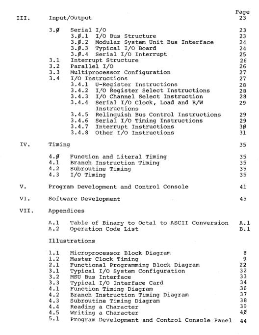
[image:4.623.66.594.60.741.2]1. SYSTEM DESIGN FEATURES
l.g. General Characteristics
The AES microprocessor is a byte oriented general purpose computer designed primarily for OEM use in dedicated applications. The main features and characteristics which describe its operation can be summarized as follows:
Instruction Memory Size - up to 4~96 l2-bit words Data Memory Size - up to 4~96 8-bit words • Tri-State Data bus
• 2k direct addressing of Instruction Memory · lk direct addressing of Data Memory
• 24~ nanosecond instruction time (full cycle) assuming all bipolar memory
• Single clock cycle (1 state) per full instruction cycle
• 6 Registers
• All modes of 8-bit ALU under software control · Easy interchange and intermix of memory types and
speeds within the same processor
· Both parallel and serial I/O capability
· 16 level automatic push down stack for routine linkage
· Comprehensive instruction set. (49 basic one word
instructions plus 43 arithmetic and logic instructions) · TTL Integrated Circuitry
• Operating Temperature ~oC to 7~oC or -55°C to 125°C depending upon grade of IC's used.
The microprocessor executes one complete instruction_during one cycle of the basic timing clock. There are no sub-cycle tlme slots, or states, used within the basic instruction cycle. Conse-quently, the power of the individual instructions are some¥!hat less than those of a higher level processor, such as a "minicomputer". However these higher level instructions are available by writing
"micro-programs" or "micro-routines" and give the flexibility of, in effect, writing an instruction set in addition to writing higher level routines.
1.1. Physical Configuration
The basic AES microprocessor is contained in one AES
modular system unit. The MSU is a standard package configuration with the capabili ty of containing 9 plug in cards. All cards are
7.9191"
x 7.35" and spaced
91.6"
apart. The cards are interconnected either by an artwork or by a wire-wrap backplane. The microprocessor MSU contains the following cards:1) Timing Generator 2) Control Logic A 3) Control Logic B
4) 1.'J24 x 8 Data Memory (RAM)
Most configurations leave a slot reserved for a maintenance and control interface card that interfaces the microprocessor to a program development and control console, thus enabling the operator to monitor and/or c6ntrol the microprocessor during maintenance, test or programming.
The remaining 3 positions can be used for a variety of functions. For example if more ROM or RAM capability is required, then a combination of these cards can be inserted into the remaining positions.
Another slot may be reserved for the serial Input/Output control card. There are two versions of this card. In the simpler version the I/O address select, data and control lines are all TRI-state* outputs and inputs. The more complex version of the I/O card is identical to the simpler one in all respects except that differ-ential line drivers and receivers are used in place of the TRI-state logic. The latter card, whose primary purpose is increasing the al-lowable load on the I/O bus, is used in cases where the I/O bus is longer than 2~ ft and/or when more than 5 I/O channels are used. The remaining two slots may be filled by two parallel I/O interface cards, or 1 interface card and one parallel I/O buffer expander. The parallel I/O buffer card is meant (as in the case of the complex serial I/O card) for increasing the allowable I/O bus loading.
The ROM memory card may be removed and in its place a ROM simulator interface card inserted. This card is used to interface the microprocessor to a ROM simulator which is a part of the program development and control console. The ROM simulator, which is actually a fast bipolar random access memory, behaves exactly as a ROM card where the microprocessor is concerned. I t is, however, possible to write
instructions into the ROM simulator via an ASR 33 TTY, or a tape reader, thus enabling the programmer to develop and ve,rify the final software before masking the program into the Read Only Memory.
1.2. System Organization
The AES microprocessor is a bus organized machine designed around a data transfer concept. An 8-bit TRI-state processor bus is used as the main highway for data traffic between registers and data memory. The source and destination of data travelling along
the processor bus is under complete microprogram control. The basic microprocessor elements are shown in the block diagram of Figure 1-1.
1.3. Instruction Memory
upon the particular instruction decoded, literal data can be out-putted directly from RO.r.1.
1.4. Data Memory
The Data Memory is available with from 1 to 16 256 word by 8-bit modules for a maximum capacity of 4,96 words. These modules can be selected from any of the following types and intermixed with-in the same processor.
Tfiee 1 High speed parallel bipolar scratch pad memory. T 1S type of 256 word memory module has a cycle time faster than the basic machine cycle time of 24~ nano-seconds. Thus data can be read out of or written into this memory during a single machine clock cycle.
Tyae 2 Non volatile random access read/write core memory mo ule. This type of memory module has a cycle time of
1 micro-second.
T*ee 3 MOS static random access read/write memory module. T 1S module is partially powered by a rechargeable battery for standby powe~ applications so that the memory remains non volatile for up to 48 hours after external power is removed.
Type 4 Bipolar read only memory module.
Type 5 Special purpose function modules.
As can be seen from figure 1-1, data is both read out of and written into data memory via the high speed 8-bit Tri-State processor bus. Thus, for real time applications, where time is at a premium, memory modules of type 1 should be used because of its speed. This type of memory module also satisfies the need for high speed general storage and working registers.
Memory module types 2 or 3 should be used in cases where momentary power failure can occur but where i t is necessary -to retain data stored into data memory prior to the power off condition.
Bipolar ROM modules may be used within the data memory bank for storing constants and other predefined data which will never be altered during a program.
1.5. Arithmetic Logic Unit (ALU)
The arithmetic logic unit operates on two 8-bit variables the tri-state processor bus and its own output buffer accumulator. The ALU is capable of performing up to 16 logic operations on its two input variables and a variety of arithmetic operations; the most important being add and subtracto The mode of the ALU is selected by the ALU command register which is set by executing a single ALU. literal instruction.
1.6. Registers
1.6.~o P-Register: The 12-bit P (Program Counter) register indicates the address of the next instruction to be fetched out of instruction memory. The P-register automatically increments by one after the execution of each instruction except in the following cases. If the previous instruction was one of the following:
- a conditional branch instruction whose jumping criteria has been met,
- an unconditional jump instruction, or
- a jump to subroutine instruction,
the least significant 11 bits of the P register are loaded with the ROM output data, thus defining the current page jump address.
Similarly if the previous instruction was a return from subroutine instruction, the P-register is loaded with the return address last stored into the push-down stack.
1.6.1. A-Register: The 12-bit A (Data Memory Address) register holds the address of the data memory cell being read from or written into. During a RAM address command, its contents may be altered and the l~-bit operand field of the instruction loaded into the least significant ].~ bits of the A register.
In ad~ition, three instructions alter the A-register so tha-t:
- the contents of the A register may be incremented,
- the least significant 8 bits of the A register may be loaded with the data present on the TRI-state processor bus, or
- the most significant 4 bits of the A register may be loaded with the 4 least significant bits of the processor bus.
1.6.3. L.A.-Register: The 8-bi t LA (ALU Conunand) register is similar to the L-register in that an 8 bit literal from ROM is loaded into i t during an ALU literal instruction. The output of the LA-register selects the operating mode of the ALU.
1.6.4. B-Register: The 8-bit B (ALU Output Buffer) register is the ALU accumulator in which all results of the arithmetic and logical operations are stored. Using the appropriate instructions, the B registei may be:
a) partially loaded by the 4 least significant bits of the ALU output,
b) partially loaded by the 4 most significant bits of the ALU output,
c) completely, loaded by all 8 output bits of the ALU,
d) rotated right by one bit, or
e) cleared.
1.6.5. u-Register: The U (Universal) register is an 8-bit parallel in, parallel out, serial in or serial out register. It is primarily used as the serial I/O buffer register. To output an 8-bit character onto the serial I/O data bus, data is loaded into the U register from the TRI-state processor bus. When an I/O output command is initiated, the data from the U-register is automatically shifted out onto the I/O data bus. The data is also recirculated back into the U-register so that the character can be retransmitted if necessary. To input a character from the I/O data line, an input command is initiated and the 8-bit character is automatically shifted into the U-register. Appropriate instructions permit the U register to be merged (inclusive "OR" ed) with the data on the TRI-state
processor bus, and also to be cleared.
The U-register is also a temporary storage buffer 'of data on the TRI-state processor bus. It is commonly used as a temporary storage for one byte of a 2 byte address' pointer (2 word indirect add~ess) from data memory.
1.7. Decision Flags
within the microprocessor there are various status flag bits which are addressed by the appropriate decision instruction. These decision flags are tested by the microprogram to determine whether (or not) a conditional branch operation is implemented.
If the decision instruction is decoded, for example, as lIbranch if decision flag 5
=
logic 1", the next instruction will be inter-preted as a jump address, or ignored, depending upon whether the1.8. Push Down Stack
'rhe AES microprocessor has a 16 level au"t:omatic push down stack which is used for routine linkage 0 When a jump to subr.outine
command is read from the instruction memory, -the contents of the P
register plus "2" is stored into the push down stack as a return address to be used when returning from the subroutine 0 After the
return address is stored, the stack is virtually pushed down so that a lower level return address may be stored. This occurs when the subroutine itself calls up yet another subroutine. The next instruction will then automatically be interpreted as a jump address defining the starting location of the subroutine., When a return from subroutine command is read from ROM, the return address will be transferred to the P register from the push down stack during the next machine cycle. When an overflow (eoge greater than 16 sub-routine levels) or an underflow occurs in the push down stack, a decision flag is set.
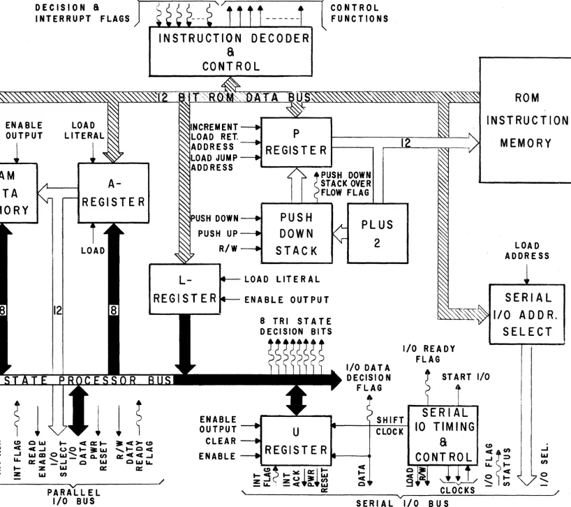
1.9. Instruction Timing
The basic clock is a 12.5 MHz crystal oscillatorD The
f~equency of this oscillator is divided down by 3, producing the
m~croprocessor master clock~ This clock has a pulse width of 8~
nano-sec. and a total period of 24~ nano-sec~ as shown in Fig. 1.2.
This period forms the basic machine cycle time and all instructions are executed wi thin this time slot. In some cases {I where the
in-struction or data memory has an access time longer than 16~ n sec, a memory ready flag from the memory device being accessed maybe used to lengthen or delay the master clock in increments of 8~ nano-sec. This feature of having a variable cycle time is normally not used. I t does, however, provide the flexibility of intermixing both slow and fast memory types within the same microprocessor
with-out completely slowing down the master clock to accommodate the slowest memory module. I t should be noted that only the leading and trailing edges of the master clock pulse are used for strobing or setting the various logic functions throughout the control ,logic of the microprocessor. No other sub-clocks delay lines or one-shots are used for timing purposes. When the P register is incremented or loaded, the new instruction address is available. After the
memory access time has been reached, data is available for instruction decoding. Both the leading and trailing edges of the next clock
pulse are used for executing the instruction just read. The detailed timing diagrams for the various instructions are provided in section
IV.
l.l~. Input/Output Interface
line. This I/O bus is used to transfer 8 bit serial characters
into or out of the microprocessor at rates up to one character every 9 .12 micro-seconds.
As soon as the selected' peripheral has been addressed, and the data to be transferred is ready either in the U-register
(for transmitting) or on the addressed I/O device (for receiving}, a start I/O instruction is executed. The clocking and transfer of I/O data then becomes automatic, with the microprocessor free to execute other instructions during the I/O interval. As soon as the I/O transfer is complete,the I/O ready decision flag is set. This enables the microprocessor to branch when I/O is complete. In
addition to the serial I/O, a parallel I/O capability is available. This is normally used as a means of providing hardware processor options such as hardware multiply/divide or sine/cosine function hardware etc.
This bus is also used as a means of accessing a large data base such as a disc or magnetic tape unit, where maximum data throughput is necessary.
The parallel I/O bus· consists of 12 address lines, 8 I/O data lines, a wri te strobe, 'a read enable line, an interrupt flag, a device ready flag and an interrupt acknowledge line. The I/O address and data lines are the same as those used for accessing the microprocessor data memory, i.e. the 8 bit TRI-state processor bus
is the same as the I/O data bus, and the A-register outputs are also the 12 addressing lines for the parallel devices. A power reset pulse is sent to all peripherals both on the serial and parallel I/O bus when the power on reset condition is present.
LOAD
LITERAL
LA-REGISTER
DECISION
a
J
INTERRUPT FLAGS
D=B FLAG
CARRY
OUT
FLAG
ENABLE
R/W OUTPUT
LOAD
LITERAL
8
BIT
F
FIG. I - I
RAM
DATA
MEMORY
- - - SHIFT
- - - CLEAR
---LOAD
---- ENABLE
1
~
MICRO PROCESSOR
~ (!)U <I:
<I: -I
La..
l-BLOCK
DIAGRAM
z
I--
Z-"
A-REGISTER
1 1 1
f
o UJ I- <I: a: I- ~c:t>(!)
<I:-J (')Ol-~IJJ ... I - o e
IJJ CD 0 IJJ ... <I: Q. (I) o:::Cc:t-J
0::: c:t ~ -J - 0 kI QUJL&..
Z LLI a:: 0:::
LLI (I)
v
PARALLEL
I/O BUS
INSTRUCTION DECODER
a
CONTROL
NCREMENT-..
LOAD RET.
ADDRESS
-
..
AD JUMP-..
( CONTROL
FUNCTIONS
ADDRESS
'---r---P"""""USH DOWN
PUSH UP-.w
R/W-...
PUSH
DOWN
STACK
L-
---
LOAD LITERAL
STACK OVER
FLOW FLAG
PLUS
2
REGIST ER---
ENABLE OUTPUT
8
TRI STATE
DECISION BITS
I/O OAT A
DECISION
FLAG
I/O READY
FLAG
ROM
INST
RU C T I ON
MEMORY
LOAD
ADDRESS
SERIAL
1/0 ADOR.
SELECT
START I/O
SERIAL
ENABLE
SHIFT
10 TIMING
OUTPUT
U
CLOCK
CLEAR
a
(!).
-I
CONT RO L
~
Sg:
kIENABLE
La.. I- In
c:t
e:)
~~~r-Q c:t
0
l- e
°11-I-
:5
I- (.) ~ kI C9
'--~ ... (I) ...z
z
(I)/ _LL: _<t a.. kI 0
CLOCKS
a: /
"
v [image:12.1229.338.1157.36.762.2]12,5 MHZ CLOCK OSC.
BASIC MASTER CLOCK
A
12.5 MHZ CLOCK
05(.
ROM ADDRESS IN
ROM
DATA OUT
B
I
jROM DATA READY FLAG
~-I
J
MASTER CLOCK
I
Ii
II
II
II
II
II
II
II
I , I I ,¢
8¢
16¢
24¢
32'/J
4¢¢
48¢
56¢
64~
72¢ 8¢¢
FIG. 1.2 MASTER
CLOCK TIMING
(A) CONSTANT
ACCESS
TIME
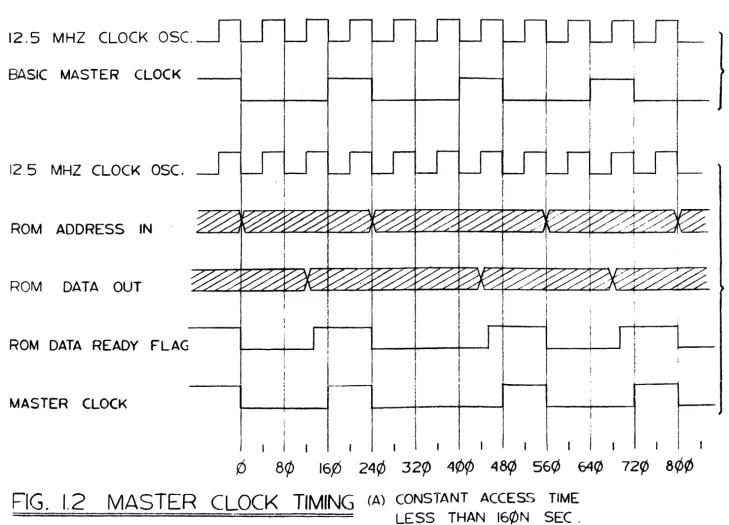
[image:13.804.31.761.638.1163.2]II. Micro-Instruction Repertoire
The AES micro-processor has 92 basic one-word instructions, all executable in 24~ nanoseconds. This section describes all of these micro-instructions. with each description is a diagram
showing the format of the command, the mnemonic used in referencing i t and also the two character ASCII code. The latter is used as the binary paper tape format when loading the ROM simulator via an ASR 33 TTY or paper tape reader.
2.~. Instruction Formats
There are six basic instruction formats. Each micro-instruction is 12 bits in length and is contained in a single read-only memory location.
The formats are for.function, decision, ROM address, RAM address, Data Literal and ALU literal micro-instructions.
2.~.~. Function
The function micro-instructions have the following format:
11 l~ 9 8 7 6 5 4 3 2 1 ~
The function type of micro-instruction is used for setting or clearing various control signals within the machine.
The simplest type of function is a latching function. In this case, execution of the instruction implies setting or clearing the logic signal defined by the function select code, depending upon whether bit 7 is a 1 or a ~ respectively. The second type of function is a strobing function. This type of instruction sets
the addressed function line for one machine cycle period only. This type of function is used for strobing latches and clocking registers etc. Bit 7 is not decoded in this case.
The third type is a mutually exclusive function. The setting of one function within a mutually exclusive group also implies the clearing of all other func·tions wi thin that group. If one mutually exclusive function is cleared, all functions within that group will also be cleared.
The last type of function is a strobe, branch type of instruction. This behaves like a strobe function, but in addition the next instruction is unconditionally treated as a branch address. The only function of this type is the jump to subroutine instruction explained in section 2.11.
2.~.1. Decision
The decision micro-instruction has the following format.
When bits 8-11 of the micro-instruction are ~, the first seven bits form a selection address to interrogate one of 27
possible decision flags. If the flag is equal to the value of bit 7, the next micro-instruction will be treated as a branch address.
2.~.2~ ROM Address
The ROM address micro-instruction has the following format:
CURRENT PAGE ROM ADDRESS , • , , , I , ,
11 l~ 9 8 7 6 5 4 3 2 1
The ROM address micro-instruction is defined by a 1 in bit 11. After the execution of a valid decision or a strobe branch function, the least significant II-bits of the next word of memory data coming from ROM is loaded into the P register. Bit 11 of the P register remains unchanged, A HOM address command located any-where else in a micro-program is ignored. The combination of a decision followed by a ROM address can be thought of as a two word conditional branch instruction.
2.~.3. RAM Address
The RAM address micro-instruction has the following format:
I
fI , 1I
CU,RRE,NT fAG,E~M ~DD,RES,S
11 10 9 8 7 6 5 4 3 2 1fI
When bits 11 and Ifl are
fI
and 1 respectively, the remain-ing bits are stored into the least significant Ifl-bits of the A register. Bitslfl
and 11 of the register are left unchanged. 2.~.4. Data LiteralThe Data Literal address micro-instruction has the following format:
LITERAL
I ,
11 10 9 8 7 6 5 4 3 2 1
fI
When bits 11, l~, 9 and 8 are
fI,
~, 1 andf1
respectively, the 8 bit literal, defined by bits ~-7, is stored into the2.~.5. ALU Literal
The ALU Literal address micro-instruction has the following format:
~ ~ 1 1 ALU COMMAND
11 If1 9 8 7 6 5 4 3 2 1 ~
In a similar fashion to the data literal micro-instruction, the ALU literal command enables the 8 bit literal defined by bits ~-7 onto the LA register.
2.1. Terms, Mnemonics and Symbols
[image:16.618.80.566.404.773.2]For example:
The modified ASCII representation of the following function
.[~,~,~,
1 1 ~ ~ Y1 ~ 1 1 111 1
fa'
9 8 7 6 5 4 3 2 1fa'
is FG.
Some of the symbols and terms used in the description of
instructions are:
JIS,xxx
JIC,xxx
#
t
A'
+
Set contents of Al equal to A
2• A2 is
left unchanged.
Jump if flag xxx is set.
Jump if flag xxx is clear.
Logical OR operation.
Logical AND operation.
Logical EXCLUSIVE OR operation.
Logical Complement of A.
Arithmetic plus operation.
Arithmetic minus operation.
The rest of section II is devoted to describing the AES
Microprocessor instructions. The detailed functional programming block diagram shown in Fig. 2.1. way be used as a guide in under-standing these commands.
2.2.
set.
Load Data Bus
Mnemonic
D=L
D=M
D=U
D=B
Instructions
ASCII
F@
FA
FB
FC
Description
Load data bus with contents of the L-register.
Load data bus with data memory output.
Load data bus with contents of the U- register.
Load data bus with contents of the B-register.
2.3. Load Literal Buffer Instruction
Mnemonic
L
=
xxx·
ASCII
HCL
Ioc. Joe.
K.«.
2.4. ALU Mode Instructions
Description
Load L-Register with octal number
xxx (xxx
may take on the valuesr-
3m).~will be one of the 64 ASCII characters li~ted in Fig. 2.1.
This group comprises the instructions for performing logical and arithmetic operations on two 8-bit quantities namely D (8 bit processor data bus) and B (B-register output), and
providing an 8 bit quantity as an output, termed F. This output may be stored into the B register by using the appropriate
instruction. The ALU mode of instructions may further be subdivided into the fOllowing groups.
Loading Instructions
Mnemonic ASCII
F=D L@
F=D' LP
F=B LZ
F=B' LU
F=-l LC
F=!1 LS
Description
Set the ALU output equal to the data bus.
Set the ALU output equal to the complement of the data bus.
Set the ALU output equal to the B-register output.
Set the ALU output equal to the complement of the B-register output.
Set the ALU output equal to minus I (2's complement), i.e. all bits of F are logic 1.
Logic Instructi~.
Mnemonic ASCII
-F=D#B LA
F=D#B' LB
F=D' #B LX
F=D' #B' LT
F=D.B L [
F:;::D.B' I.lW
r=D'
.B LRF=D' • B' LQ
F::;:DtB
LV
F=DtB' LY
Arithmetic Instructions
Mnemonic ASCII
F=D+D LL
F=D+B LI
F=D+D+l L,
F=D+B+l L)
F=D-B L&
Description
Set the ALU output equal to the logical or of D and B.
Set the ALU output equal to the logical or of D and ~
Set the ALU output equal to the logical or of
5
and B. Set the ALU output equal to the logical or ofD
andB.
Set ALU output equal to the lo~ical and of D and B. Set ALU output equal to the logical and of D and B.
Set ALU output equal to the logical and of
IT
and B.Set ALU output equal to the logical and of
5
and B. Set ALU output equal to the exclusive or of D and B.Set ALU output equal to the exclusive or of D and
B.
Description
Set ALU output equal to D plus D.
Set ALU output equal to D plus B.
Set ALU output equal to D plus D plus 1.
Set ALU output equal to D plus B plus 1.
Mnemonic ASCII Description
F=D-B-l LF Set ALU output equal to D minus B minus 1.
F=D+l L(space) Set ALU output equal to D plus 1.
F=D-l LO Set ALU output equal to D minus 1.
Combined Logical and Arithmetic Instructions
In the following qroup of instructions, i t is assumed that logical operations are done before the arithmetic ones.
Mnemonic
F=D#B+D
F=D#B'+D
Mnemonic ASCII
F=D#B+l L!
F=D#B+D+l
L-F=D.B+D LH
F=D.B+D+l L(
F=D.B-l LK
F=D#B+D.B' LE
F=D#B+D.B'+l L%
Shift Rotate Instructions
Mnemonic ASCII
F=BSL LL
F=BRL ML
EBR N@
ASCII
LM
LN
Mnemonic ASCII
F=D#B'+l Lit
F=D#B'+D+l L.
F=D.B'+D LD
F=D.B'+D+l L$
F=D.B'-l LG
F=D#B'+D.B LJ
F=D#B'+D.B+l L*
Description
Set thp ALU output equal to
the B-register shifted left one bit. The LSB of the ALU output is set to ~.
Set the ALU output equal to the B register rotated left one bit. Thus the LSB of the ALU output is equal to the MSB of the B-register.
Set the B-register into the rotate mode.
2.5. Load Accumulator Instructions
Mnemonic ASCII
B=f6 PH
B=F FI
B=FH FJ
B=FL FK
B=BRR FI
Description
Clear the accumulator or B-register.
Load the B-register with the output of the ALD.
Load the B-register's most significant 4 bits with those of the ALU output. The least significant 4 bits of the B register are left unchanged.
Load the B-register's least significant 4 bits with those of the ALU output. The most significant 4 bits of the B-register are left unchanged.
Rotate the B-register right one bit.
These instructions all fall under the category of strobe functions. The last preceding ALU Literal command before a B=BRR instruction must be EBR. On the other hand, the last preceding ALU Literal before B=F, B=FH or B=FL must not be EBR. B=~ will clear the accumulator in both cases.
2.6. RAM Address Instructions
Mnemonic ASCII
A=xxx
AL=D FE
AH=D FF
Description
Load A register with address xxx (xxx is the l~ bit RAM . addreSS-and may take on the
values {6 - 1777 8).
Depending on the address chosen,~ will be one of the following
ASCII characters:
(P, Q, R, S, T, U, V, W, X, Y,
Z, [ " ,] , t , or +-) and j3 \vill be one of the 64 ASCII characters
listed in Appendix 1. Bits lf6 and 11 of the A-register are left unchanged.
The data bus is loaded into the 8 least significant bits of the A-register. Bits 8, 9,
1,
and11 of the A-register are left un-changed.
A=A+l F:
~, 1, 2 & 3 of the data bus . respectively.
Increment the contents of the A-register.
2.7 Store Into RAM Instruction Mnemonic ASCII
M=O FL
Description
Load data bus into RAM. The address in RAM must be previ-ously defined by a RAM address instruction. The data memory is normally in the read mode and the M = D instruction, which is a strobe function,
sends a write pulse to the
RAM for the duration of the machine cycle.
2.8. Conditional Branch Instructions
This group comprises the ins·tructions that direct the
program to a nonsequential address for execution of the instruction located there. As previously shown in section 2.~.1, bits ~ to 6 of the ROM data define which of the possible 27 decision flags will define the logical condition for execution of the jump. The jump address is contained in the next word from instruction memory. Each of the following branch instructions comes in complementary pairs, i.e. jumping when the decision flag is either set or ·cleared.
Mnemonic JIS,BR7 JIS,CRY JIS,D=B JIS,DB~ JIS,DBI JIS,DB2 JIS,DB3 JIS,DB4 JIS,DBS JIS,DB6 JIS,DB7 Mnemonic
for
compIement JIC,BR7 JIC,CRY JIC,D=B JIC,DB~ JIC,DBI JIC,DB2 JIC,DB3 JIC,DB4 JIC,DBS JIC,DB6 JIC,DB7ASCII ASCII Description
for
Comprement
BC @C Jump if B-register bit 7 is Set/Clear ..
BD @D Jump if ALU carry output flag is Set/Cleare This flag is a "I" when there is an overflow or under-flow during an ALU addition or subtraction respectively.
BE @E Jump if data bus and B-register are equal/not equalo ALU must be in F=D-B-l mode. (see pg.16) .
BH @H BI @I
BJ @J Jump if bit n of the BK @K data bus is set/clear BL @L where n = .~ to 7
Mnemonic
JIS,PDS
Mnemonic for Comprement
,-TIC, PDS
ASCII
BW
ASCII Description
for comprement
@W Jump if push down stack
overflow flag is Set/ Clear. This flag is set when the 16 levels of push down stack are either overflowed or underflowed. It is automatically cleared when the microprocessor
is in the PORe condition. Thus, a reset instruction will clear it. (see
pg. 22).
The rema1n1ng conditional branch instructions are described in the section on Input/Output.
2.9. Set Page Instructions
As shown in Section 2.~.2, the least significant II-bits of a ROM address instruction enables the direct addressing of 2~48
memory locations. For addressing all the 4~96 locations, the following instructions should be used.
Mnemonic ASCII
PG=yY DT
PG=1 FT
Description
The most significant bit (bit 11) of the parallel input to the P-register is set to~. This means that the next valid decision to take place will cause a jump to page ~ of the instruction memory. The page is always set to ~
automatically after power goes on.
Bit 11 of the P-register parallel input is set to 1 so that the next branch will be to the upper page of instruction memory.
It should be noted that a PG=~ or PG=1 instruction does not change the page at the time of the command, but rather defines the page to be jumped to at the next branch.
2.l~. Unconditional Jump Instruction
Mnemonic ASCII
JMP B@
Description
This instruction causes an uncon-ditional jump to the ~ddress
2.11.
2.12.
2.13.
Jump to Subroutine Instruction
Mnemonic ASCII
JSR F{I
Description
This loads an address two greater than that in the P register into the push down stack6 After this return address is stored, the stack is pushed down ready to accept another return address. The next instruction from ROM will be treated as an uncondi-tional branch address to which the P register will be seto This instruction is a strobe branch function.
Return from Subroutine Instruction
Mnemonic ASCII
RET FN
Description
This instruction causes the push down stack to "push up", thus revealing the last return address stored into it. This return
address is then enabled onto the P register parallel input.
In addition to the next instruction from ROM being executed, the return address will be loaded into the P register causing a return jump to the subroutine calling program.
Nap and HALT Instructions
Mnemoni.c NOP HLT=, HLT=l HLT=2 HLT=3 HLT=4 HLT=S HLT=6 HLT=7 HLT=l, HLT=ll HLT=12 HLT=13 HLT=14 HLT=lS HLT=16 HLT=17
ASCII Description
@@ No operation is performed by this instruction except that a one machine cycle delay of 24~ nG seconds results.
F(space) If a maintenance and control
F! chassis is interfaced to the micro-F" processor, anyone of the 16 HALT F# instructions will stop the pro-F$ cessor master clock. In the case F% where no maintenance and control F& chassis is connected to the micro-F' processor all HAIJT instructions F( are ignored and treated as NOPs.
2.14. PORC and the RST Instruction
The PORC or power on reset circuit is used to provide the required hardware initialization when first turning the microproces-sor on. When power is firs·t turned on, PORC condition exists with-in the microprocessor for approximately l ' J milli seconds. During this condition the following is done.
a) The master clock oscillator is disabled from the microprocessor.
b) The P and A registers are cleared (set to address ~). c) A power reset pulse is sent to all peripherals both
on the serial and the parallel I/O bus.
d) The instruction memory page funct~on is set to J. e) The CLK, LD, R/W and RBC functions are all cleared.
These functions will be explained in the section on Input/Output.
f) The interrupt acknowledge function is set to ~.
g) The push down stack is set to subroutine level ~ and the overflow PDS flag is cleared.
h) The master interrupt flag is disabled.
The PORC condition may also be initiated in two other
ways. The first way is to press the reset button on the maintenance and control chassis, assuming i t is connected to the microprocessor. The second way is to execute a reset instruction.
2.15.
Mnemonic ASCII
RST F8
Description
Strobe the microprocessor into the PORC condition.
Real Time Clock and the RTC Instruction
The real time clock provides the setting of the decision flag at a crystal-controlled timing rate. The timing is derived from the microprocessor internal master clock which is divided down by some integral number as determined by optional strapping. This clock frequency may be strapped into the master interrupt circuit
(see sec. 3.1.) for use in interrupt mode, or may be used as a decision flag to be detected under program control. Although only one decision flag (RTC) is mentioned, more are available as an option.
Mnemonic Mnemonic for Complement Instruction
JIS,RTC JIC,RTC
ASCII ASCII for
ComElement Instruction
BF @F
Description
SERIAL 1/0 8US PARALL EL lI0 8 U S
/~ _ _ _ _ _ _ _ _ _ _ _ _ _ _ _ _ _ _ _ _ _ _ _ _ _ _ _ _ _ _ _ _ _ _ _ _ _ _ _ _ _ _ _ _ _ _ _ _ _ _ _ _ _ _ _ _ ~A~ _ _ _ _ _ _ _ _ _ _ _ _ _ _ _ _ _ _ _ _ _ _ _ _ _ _ _ _ _ _ _ _ _ _ _ __ _ _ _ _ _ _ _ _ _ _ _ _ _ _ _ _ _ _ _ _ , /~---~A~---~,
INT CLOCK CLOCK OUT IN
...-(-Ci.-K~
( CLK=' )
7
J
I/O READY1/0
I
II/O CLOCK PT TIMING CONTROL I/O I/O CLOCK START INT
J
I.
~~
R/W~
DATA-~
(R/~
( R/W = R J
2; - 22 27
It'
/V;
3
.L.
SERIAL 110 SELECT
/,,-_ _ _ _ _ _ _ _ _ _ _ _ _ _ _ _ _ _ _ _ A ' -_ _ _ _ _ _ _ _ _ _ _ _ _ _ _ , tNT ER R U PT
REGISTE R NO
~~~
~~~~~ ~
ACKCHANNEL NO LOAD
,
I 2 3 4 5 6 7SERIAL 1/0
POP INT FLAG
~
){){
I/O I/O SELECT DATA
~l;Q
v V
/ 12/ 8
R/W
A
READ ENABLE
I?
FLAG INT
Il){"
INT ACKS
,
RG=B )-t REGISTER H RG=lC )
SERIAL 1/0
CHANNEL SELECT
(IAK1:1 (LO= I ) ( ___ ,-RS,-,T~ ( RBC ) ( RST ) ( M;:O J O=M PFL PIN
CJAK";D
B NO
~
'"
.
,.
3/
LA IN ENABLEH F=X )
LA- REG I STE R EIN }-t
2' 25 24 23 22 21 2~
~
to
B
..
jJ
8 elN M S3 S2 SI S" D
~
D:B
8-BIT ALU
~
CARRY OUT
t:'
'\ 8
B = BR R ) ( EBR
~
J
\..~
ROTATE BIN LOAD/SHIFT
t B=FL )-t LOAD LOW LOAD 4-{ B."F
B-REGISTER
( B= FH
r
LOAD HIGH CLEAR 4-{ B = 0 BOUT( IAK =(J J ( LD=0 J l EBC )
&
1
(CHL=XX
INSTRUCTION DECODER 8
CONTROL
~ ~ ~---~
11---1
DECISION a INSTRUCTION INTERRUPT CONTROLFL AG
( L=XXX
I
A =Aft )
MI N R INCR _____ _
A SEL R H A=XXX ')
RAM ADDRESS~2[111 AOUT REGISTER. __ _ SEL D H AH -;;0) MOUT R/W S~~wD D HI
1
T £ ~8' ,( M=O ) ( AL=O)
v (IAK=0)
I
( PG = I ROM
( PG =0 )
8/ 2"-27
LIN ENABLE L
RET )---t R/PDS P LS.
~~
REGISTER
~
LOUT
}
1 __ _
W
DOUT DIN 4-BIT UP DOUT 16-WORD PUSH DOWN COUNTER ADD DOWN STACK
DOWN UP : R/W
( RET) JSR) ( JSR )
SIO )
(-6 >----+.--t---+---V-:6---o-,
~----~
CLOCK~--_--I----
UOUT 8 ...,.
... SER. IN
----
SER.OUTU - REGISTER D=U 0= B )
U=U#D SET ENABLE ( D=M
( U=0 CLEAR UIN
A
t
'",.
~ ~ ....
"\~
,
.. 0 8,.. BIT -.I.R ---.S.IA.LE ~ROCES S 0 BUS~
~~~~~~~~
~~~?
[image:26.1230.97.1174.32.723.2]III. Input/Output
The AES Input/Output system provides a powerful and flexi-ble interface between the microprocessor and the peripheral devices
that are connect to it.
The I/O system may be subdivided into two principal parts namely (a) serial I/O and (b) parallel I/O. A typical I/O system configuration is shown in Fig.3-1.
3.fI.
3.~.1.
Serial I/O
I/O Bus Structure
The I/O bus that interconnects the microprocessor to the external device has the following structural elements:
a) Address: 8 lines defining an 8 bit I/O select code for addressing up to 256 8 bit registers. 5 lines are used for defining one of 32 channels and the
remaining 3 are used for selecting one of 8 registers within the channel.
b) Control: 5 lines called LOAD, R/W, CLOCK, IAK and POP. The first three signals control the transfer of data to or from the external device and the fourth signal acknowledge an interrupt request. The POP signal is the power on pulse generated during a PORC condition.
c) Flags: A status flag corresponding to the I/O select code may be read on one line of the I/O bus. A serial I/O interrupt flag line is also available. This is the logical "OR" of all the interrupt flags within the system.
d) Data: One bi-directional line is available on the serial I/O bus for transferring 8-bit serial characters to or from the microprocessor.
e) Propagation Delay: Two additional clock lines exist within the seriaT bus. This permits the reading of
serial data into the microprocessor to be independent of the physical length of the bus. The clock which is used to shift I/O data through the U-register is "transmitted" onto the I/O bus from the microprocessor and "reflected" from the addressed peripheral. The return clock line is then used so shift serial data into the U-register.
Type 1: For simple systems (maximum of 2 I/O channels, proximity of less than 5 ft.), all unidirectional bus lines use standard TTL gates as both drivers and receivers and bi-directional lines use TRI-state'* TTL logic gates as drivers and standard TTL gates as receivers. For this system configuration no serial Input/ Output control card is necessary.
Type 2: For medium sized systems (maximum of 5 I/O channels, proximity of less than 2~ ft.) all bus lines use TTL TRI-state gates for both drivers and receivers. Each signal
line
is twisted with a ground line to form a twisted pair.Type 3: For large systems, using more I/O than types 1 and 2, all bus lines make use of "Party Line" differential line drivers and receivers. These drivers are able to drive up to l~~~ ft. of bus line at standard TTL speeds.
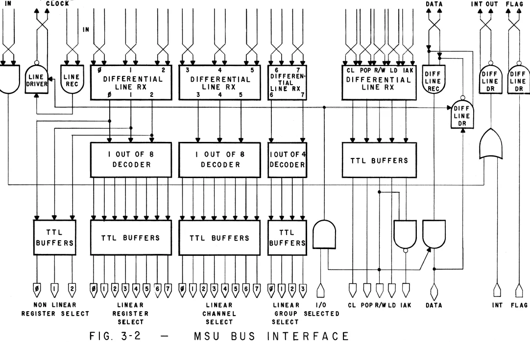
3.~.2 Modular System Unit Bus Interface
The modular system unit (MSU) bus interface card is designed to interface up to 8 I/O peripheral interface cards to the microprocessor serial I/O bus (see Fig.3.2). This card is intended for use in systems of type 3 and its primary function is to interface the differential driver and rec~iver signals to standard TTL logic levels. This card also decodes the eight address select lines to form 4 group, 8 channel and 8 register linear select signals for enabling the I/O cards within the modular system unit.
The I/O devices within the MSU provide an I/O selected signal which indicates if one of them has been addressed. When this signal is high~ the I/O flag status is enabled onto the I/O bus. When the I/O selected line
is
high and, in addition, the R/W line is in the read condition, both the data line and micro-processor I/O clock are enabled onto the I/O bus.3.~.3 Typical I/O Board
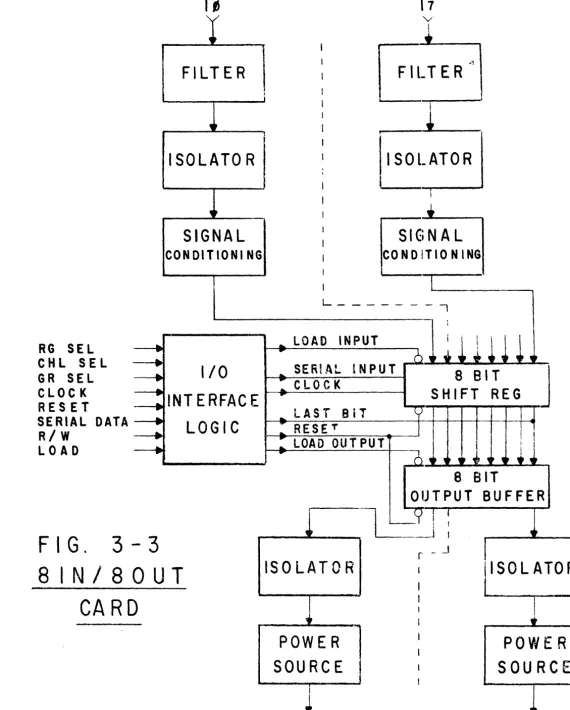
A typical MSU module contains 9 I/O cards which communicate with an AES microprocessor through an MSU bus interface card. A
typical example of the type of I/O cards is an 8 IN/8 OUT card. The block diagram of such a card is shown in Fig.3-3. The
following is a description of the functions of the various block interconnections~
The 8 IN/8 OUT provides the following capabilities:
1) Reading status of 8 external points and inputting the information to the microprocessor.
2) outputting drives (sinks) to 8 external points
The inpu·t and output of this information is under complete microprocessor program control.
The block labelled I/O INTERFACE LOGIC provides the media of interpreting microprogrammed sequences as well as decoding the destination address of these sequences~ The address decode is a strappable option. Consequently, if a string of commands
contains the address of the 8 IN/8 OUT board then READ/WRITE action is initiated depending on the request 0 For example, if the request is to read status from 8 external points then the 8 points in
question are strobed into the 8 BIT SHIFT REGISTER and a second sequence would automatically shift the dat.a onto the serial I/O bus and into the microprocessor. Similarly the outputting of data follows the same pattern.
Several other features are provided for by the card. Consider first the 8 input lines. The status input lines are isolated from the logic with photocoupled isolators. This separates the logic from any power or ground line noise induced on the status lines. Furthermore, each line has an input filter which can protect agains·t induced electrical transients (up to 3.5kV). A third feature is provided in the signal conditioning circuitry. This basically prevents any slowly changing status signals from causing the logic to operate in its linear region. Linear region operation would generate oscillations in the logic.
The output lines are also isolated from the logic and
are protected against electrical transients. An important feature for the outputs is the capability of providing either a source of power for the 8 external points or of sinking current from these same 8 sources. This source/sink capability is an option on the card.
3.~.4 Serial I/O Interrupt
All I/O interface cards within a Modular System Unit having an interrupt flag, output this signal which is logically "OR"ed within the MSU to form the interrupt flag line. The
interrupt flag lines from all Modular System Units are, similarly, logically "OR"ed to provide the serial I/O interrupt flag to the microprocessor.
3.1 Interrupt Structure
Eight decision flag bits are provided to designate a
particular interrupt condition. When any of these bits are high, the master interrupt flag goes high. The master interrupt flag bit may be tested by the microprogram to detect the interrupt condition. When the microprocessor has recognized the interrupt request, i t may respond accordingly.
The normal procedure for acknowledging an interrupt is to regularly monitor the master interrupt flag. This can be done by executing a decision instruction on the interrupt flag whenever returning from a subroutine. One must assume, of
course, that the maximum allowable interrupt response time is not exceeded by the maximum subroutine execution time.
Normally, the interrupt flag is low and only 2 machine cycle times (48. n seconds) are wasted looking at the flag. If, however, the flag is high, the microprocessor can proceed to execute an interrupt servicing routine which checks the 8 interrupt flags in order of their priority.
The master interrupt flag may be disabled or enabled by using the appropriate instructions.
Once the flag responsible for generating the interrupt is found, i t may be serviced. The interrupting flag should, however, be cleared prior to servicing the interrupt so that higher level interrupts may be monitored whil~ servicing the lower level one.
Decision flags may be assigned to be interrupt status
flags by strapping them into the master interrupt circuit. Flags normally assigned as interrupts are:
Push Down Stack Flag Console Alarm Interrupt Power Fail Interrupt Relinquish Bus Flag
Parallel I/O Interrupt Flag Serial I/O Interrupt Flag Real Time Clock Flag
3.2 Parallel I/O
As explained in section l.l~, the data memory and parallel I/O peripherals share the same high-speed bus. Thus the micro-processor views parallel I/O peripheral devices as active memory locations which perform special functions. There are some
differences, however, between the way the data memory and the parallel I/O devices are operated upon by the microprocessor.
It may be seen in Fig. 2.2, there are 3 control and 2
flag lines on the parallel I/O bus that are not used for accessing data memory. These are:
a) POP: Power on pulse generated during a PORC condition.
~is used for resetting all I/O devices.
b) PFL: I/O status flag usually indicates that I/O device being addressed is ready.
c) PIN: I/O interrupt flag used to indicate that at least
one
I/O device is interrupting.d) IAK: Interrupt acknowledge signal used for clearing the interrupt flag of the I/O device being addressed.
e) RBC: This line does not go onto the I/O bus, but rather, is used to disable the microprocessor from both the serial and parallel I/O busses.
In some cases the parallel I/O status flag may be used to delay the master clock until the device is ready, as explained in section 1.9.
3.3 Multiprocessor tonfiguration
A capability exists whereby the AES microprocessor can disable itself from both the serial and parallel I/O busses.
When a relinquish bus flag is sensed during an interrupt acknowledge routine, i t is possible to disable all I/O line drivers and
receivers from the I/O busses by executing a relinquish bus control instruction. This command is useful when there are 2
micro-processors on the same bus and where one of them is waiting on standby to take over bus control in the case of microprocessor failure.
3.4 I/O Instructions
The I/O instruction group is used for all communication between the computer and the peripheral devices that supply and receive data.
3.4.1
3.4.2
U-Resister Instructions
Mnemonicm ASCII Descrietion
U=~ FG Clear the U-Register (serial I/O register).
U-U#D FD Form the logical "OR" function of the D bus and U-register words and store this into the U-register.
I/O Resister Select Instruction
Mnemonic RG=~ RG-l RG-2 RG=3 RG=4 RG-5 RG-6 RG=7 RG=B ASCII FX FY FZ F[ F\ FJ F1 F4-FM Description
Set the least significant 3 bits of the serial I/O select address to the octal number n where .n = ~ to 7. This
defines the serial I/O register number.
Set the least significant 3 bits at the serial I/O select address equal to the least significant 3 bits of the B-register output.
These instructions form a mutually exclusive function set.
3.4.3. I/O Channel Select Instruction
The following instructions set the most significant 5 bits of the serial I/O select address to the number N, where N - ~ to 31. This defines the serial I/O channel number. Mnemonic CHL=~ CHL=l CHL=2 CHL=3 CHL=4 CHL=5 CHL=6 CHL=7 CHL=8 CHL=9 CHL-l~ CHL=l1 CHL=12 CHL=13 CHL-14 CHL=15 ASCII G@ GA GB GC GO GE GF GG GH GI GJ GK GL GM GN GO
Mnemonic ASCII
CHL=l6 GP
CHL-17 GQ
CHL=18 GR
CHL=19 GS
CHL=2~ GT
CHL=21 GU
CHL=22 GV
CHL=23 GW
CHL=24 GX
CHL=25 GY
CHL=26 G?
CHL=27 G[
CHL=28 G\
CHL=29 GJ
CHL=3~ G1'
3.4.4
3.4.5
3.4.6
Serial I/O CLOCK, LOAD
Mnemonic ASCII
CLK=fI DU
CLK=1 FU
LD=~ DV
LO-l FV
R/W=R DW
R/W=W FW
These instructions are
Relinguish Bus Control
Mnemonic ASCII
RBC FP
EBC DP
JIS,RBF BP
JIC,RBF @P
and R/W Instructions
Description
Clear the I/O clock line Set the I/O clock line Clear the I/O load line Set the I/O load line
Set the I/O R/W line to ~ (read) Set the I/O R/W line to 1 (write)
all latching functions.
Instructions
Description
Disable all serial and parallel I/O line drivers and receivers
Enable all serial and parallel I/O line drivers and receivers. These are automatically enabled during a PORC condition.
Jump if relinquish bus flag is set.
Jump if relinquish bus flag is clear.
Serial I/O Timing Instructions
Mnemonic ASCII
SIO
Fa
Description
Start the automatic transfer of serial data between the U-register and the addressed serial I/O device. Data will be transferred into or out of the U-register depending on the status of the R/W line.
This is a strobe function.
3.4.7
Mnemonic
JIS,IOR JIC,IOR
ASCII
BB @B
Interrupt Instructions
Mnemonic
JIS,SIN JIC,SIN
JIS,PIN JIC,PIN
DIN
EIN
JIS,INT JIC,INT
IAR=l IAI<=~
ASCII
BQ } @Q
BS @S
DQ
FQ
}
BU }
@U
FR DR
Description
Jump if the I/O ready flag is set/clear. This flag is nor-mally high. As soon as the
SIO instruction is executed, the lOR flag goes low and
remains there until the transfer of data is completed.
Description
Jump if the serial interrupt flag is set/clear.
Jump if the parallel interrupt flag is set/clear.
Disable the master interrupt
Enable the master interrupt
Jump if the master interrupt is set/clear.
Interrupt acknowledge. This latching function is used for setting or clearing both
serial and parallel interrupt and/or status flags. In order to clear a serial interrupt or status flag, the interrupting I/O device must be addressed and the R/W line equal to
3.4.8 Other I/O
Mnemonic
JIS,IOD JIC,IOD
JIS,SFL JIC,SFL
JIS,PFL JIC,PFL
JIS,ALM JIC,ALM
JIS,PWR JIC,PWR
Instructions
ASCII
BG }
@G
BR }
@R
BT
}
@T
BA
}
@A
BV }
@V
Description
Jump if serial I/O bus data line is set/clear.
Jump if serial I/O status flag is set/clear.
Jump if parallel I/O status flag is set/clear.
Jump if external alarm is set/ clear. This alarm flag decision line is not part of the serial or I/O bus but is reserved for I/O independent purposes such as operator interrupts or console alarms.
Jump if the power fail interrupt flag is set/clear. This flag should be connected to the "Power supply on" signal
available in some power supplies. This signal is the result of
12-81T
PARALLEL
I/O
ADDRESS
HARDWIRE
MULTIPLY
DIVI DE
OPTION
DISC TAPE
OR
DRUM UNIT
~
~,...---,,-
...
DATA
FLAG
~I~N~T=E~R~FA~C~E~~_~,~~~ ~-+
_ _~~-.
~
~
~
BOSE
~'-''''~
CHAUDHURI
.A ~ERROR
~.~~~--~
1 - -_ _ _CODE
~-
l'LG~E~N~E~R~A~J~O~R-r~
__
~~~~ ~-+--r--r~
~
"
~
A _ A"\ ~
_L~
CRT
~,,",",,C R i DISPLAY
~
I NTE R
:::::===========~
--
___
~ ~
FACE
~_---~-lNTERRUPT
FLAG
U - REGaSTER CLOCK RETURN
U"~E6ISTER CLOCK OUT
I'
,r
,r
I
t/O CLOCKMICRO
PROCESSOR
~/O INTERRUPT ACt< l.OAOI/O R/W
-POWER RESET
~rpULSE
uv
",
.,
r,
BUS INT.
"#
1
AID USU
,,,
h
n
h
~lANALOG
INPUTS
FIG, 3-1: TYPICAL I/O
SYSTEM CONFIGURATION
•
~ r--~..
-" \7
,r,
r,
r,
tV
n
\J
,.,
"
I 1r'r
BUS
INT. #2
r--~BUS INT.
#]
I---COMMUNICA-
DIGITAL
TIONS MS U
1/0 MSU
J~ n~
.
~ ~ ~.,r
,. ,.
,r
FULL
DUPLEX
DATA
COMMUNICAT
IONS
DIGITAL
INPUTS
~OUTPUTS
INT.
MICROPROCESSOR
1/0 BUS
IN
INTERN AL
CLOCK
DATA
I NT OUT
FLAG
IN
t)
A
t)
Q
~ ~ ~
-i!
t:i1!/f
LINE
~DRIVER
LI N E
REC
DIFFERENTIAL
LINE RX
DIFFERENTIAL
LINE RX
01 F F E
REN-TIAL
LI N
E
RX
~~
CL POP R/W LD IAK
DIFFERENTIAL
LINE
RX
"
01 F F
LI N E
REC
,
I
2
3
4
5
6
7
~~-+---~--~---+---+---~--~----~====~--=+=====F=9~+=~~----~~~~~F~
LI N E
DR
"
"
"
lOUT OF
8
DECODER
lOUT OF 8
DECODER
"
"
IOUTOF4
DECODE R
, " "
~, ~",
" " " "" """.""''1'"
~"~,,
"
TTL
BUFFERS
"
I
2
NON LINEAR
REGISTER SELECT
TTL BUFFERS
TTL BUFFERS
TTL
BUFFERS
fIl
I
2 3 4 5 .6 7
,
I
2 3 4 5 6 7
rJ
I
~
3
LI N EAR
REGIST E R
SELECT
FIG. 3-2
LINE A R
CHANNEL
SELECT
LI N EAR
I/O
GROUP SELECTED
SELECT
MSU BUS INTERFACE
.4~
"
"
"
"
.,
TTL BUFFERS
CL POP R/W LD IAK
DATA
~
DIFF
LINE
LINE
DR
DR
I
[image:37.1224.89.1171.58.757.2]RG SEL
CHl
SEL
GR
SEL
CLOCK
RESET
If}
r
FILTER
~,
ISOLATOR
~.
SIGNAL
CONDITIONI NG
I/O
----all NT E RFAC E
SERIAL DATA---
LOG Ie
RI
W
LOAD
FIG. 3-3
81N/80UT
CARD
!
:
I
7
'v'
I
~LTER"
I
,
!
+
'ISOL~TOR
I
I
I
~jNAL
IC
0 N 0 il T ION I NG
IL _ _ _ _ _ _ _ ,
LOAD
INPUT
SER~AL
INPUT
CLOCK
LAST BiT
RESET
LOAD OUTPUT
8 BIT
SHIFT REG
8 BIT
OUTPUT BUFFER
r -. -,
ISOLATOR
ilSOLATOR
I
1
/
POWE R
SOURCE
I
~
S~
l
POWE R
SOURCE
••
[image:38.1236.593.1163.42.752.2]IV. Timing
The AES microprocessor operates on a basic 24~ nano-second machine cycle. That is, a full execution cycle (read in-struction from memory and execute inin-struction) is performed in each 24~ n. second time interval (except in some special cases in which the period is extended: these cases were discussed in section 1.9). The timing diagrams presented in the following sections each correspond to a small program listed at the bottom of the diagram.
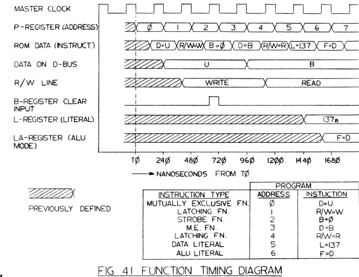
4.~ Function and Literal Timing
The program shown on figure 4.1 consists of a series of function and literal instructions. These are listed in an order which will demonstrate the strobing and latching properties of the command.
4.1 Branch Instruction Timing
The program shown in figure 4.2 consists of a series of unconditional and conditional jump instructions. The F
=
D - B-1 and D=
B commands are used in order to set the D=
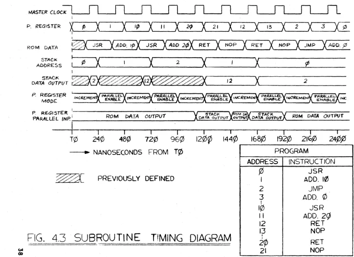
B flag high.4.2. Subroutine Timing
The program shown in figure 4.3 illustrates the execution of a routine having 2 levels of subroutine. Both jumps and returns from subroutine are demonstrated.
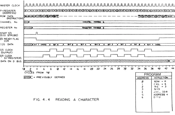
4.3. I/O Timing
Two I/O routines are illustrated. The first~figure 4.4~ reads an a-bit character into the microprocessor from a serial I/O device. It is assumed that the character being read has already been loaded into the external device transfer register. The serial I/O is first set into the read mode and the channel and register are chosen. The reading is started by a start I/O instruction and the character is automatically shifted into the V-register. The microprocessor then runs in a small program loop waiting for the I/O ready flag. As soon as this flag is set, the contents of the V-register is enabled onto the data bus where i t may be used for program requirements.