International Journal of Innovative Technology and Exploring Engineering (IJITEE) ISSN: 2278-3075,Volume-8 Issue-6, April 2019
Abstract: With the rise in tiny computing devices communicating end-to-end, followed the demand to reinforce security while not compromising on the constraints like area, power, memory, performance, latency etc. Lightweight cryptography is ideal for satisfying security requirements in resource constraint devices. LiCi is one of the recent lightweight ciphers with moderate emphasis on security for low-area overhead and low-power applications. In this paper, three different hardware architectures for this lightweight algorithm are proposed. The architectural strategies include a serialized architecture, a reduced datapath architecture and a pipelined architecture. The serial architecture consists of serially performing the operations with fewer resources using a control circuit targeting low-area and power at the expense of increased latency and low performance. The reduced datapath architecture targets a reduction in the width of the input bits for low-area and low-power with tradeoffs in security due to memory-based key-scheduling. The pipelined architecture targets high performance and throughput by reducing the critical path delay with the inclusion of registers at appropriate intervals. The proposed hardware designs target Xilinx FPGA platforms like Spartan 3, Virtex 4 and Virtex 6. The synthesis and implementation of the designs for Post Place and Route is done in Verilog using Xilinx ISE 14.6. The simulations for the same are observed in ISim Simulator. The power consumption is estimated using XPower analyzer. A fair comparison is performed with the existing ciphers in terms of slices occupied, latency, throughput and dynamic power for the targeted FPGA platforms. The dynamic power consumption of the proposed architectures is compared with the previous results for a clock frequency of 10 MHz for Virtex 6 FPGA. Among the three designs, reduced datapath design consumes the least dynamic power followed by the serial architecture.The pipelined architecture occupies higher power due to the increase of registers and clock transitions.
Keywords: LiCi cipher, IoT, RFID tags, Feistel Network, Security, Lightweight Cryptography, FPGA, Verilog, Slices.
I. INTRODUCTION
With the emergence of IoT (Internet of things), pervasive computing has increased to exponential levels. The devices interacting and communicating with each other are not limited to inanimate objects [1]. Recently introduced concepts like smart home, smart grid, smart city, ambient intelligence etc. are among the popular applications of IoT. This has led to a paradigm shift in the information transfer among the massive communication networks involving huge data transfer making the world a global village [2].
However, with this evolution came the need to constantly safeguard the data against security breaches. Any leakage of data can have severe and irreversible effects. Hence, itis also
Revised Manuscript Received on April 08, 2019.
Nigar Ayesha, Electronics and Telecommunications Engineering
Department, National Institute of Technology Raipur, Raipur, Chattisgarh, India.
BibhudendraAcharya, Electronics and Telecommunications
Engineering Department, National Institute of Technology Raipur, Raipur, Chattisgarh, India. *Corresponding Author
crucial to protect the data against potential threats by employing suitable cryptographic algorithms [3]. While popular ciphers like Advanced Encryption Algorithm (AES), Data Encryption Standard (DES) are excellent in providing tight security, the area requirements of these ciphers are not ideal for applications having constraints on the resources to be utilized.The same can be said to be true for embedded applications like Radio Frequency Identification (RFID) tags, sensor nodes and other distributed control systems where the devices are tiny with fixed resources. For example, RFID tags, smart cards require low-area and power with little emphasis on throughput. On the other hand, RFID reader device is tasked with reading out many devices at one go. Hence, in this case, higher throughput is significant with area and power not set as the deciding factors. In such applications, security is necessary but not as strict as the objectives in desktop-server environments [4].The domain of Lightweight cryptography, a subdomain of Cryptography serves the purpose of imparting adequate security as well as satisfying the criteria set on the resources [5]. Lightweight cryptography offers choices among the cipher algorithms to choose from constraints like area, power, latency, throughput, key-size, block-size and security objectives. The selection of the constraints based on the resources and security can result in a trade-off among the lesser important parameters. As a result, this makes each hardware design for a cipher to be application-specific, suitable to serve the specific purpose [6].The cryptographic structures are generally classified as SPN (Substitution-Permutation Networks) and Feistel networks. SPNs consist of a link of connected mathematical operations with a single round composed of a substitution layer and a permutation layer along with the key-scheduling. The substitution layer aims to provide confusion by mixing-up the relation between the plaintext and the key. The permutation layer is tasked with imparting diffusion by targeting major changes in the ciphertext for a minor change in the plaintext bits [7]. Examples of SPNs are PRESENT [8], Light Encryption Device (LED) [9], AES [10], RECTANGLE [11] etc. On the other hand, Feistel networks operate on one half of the input data in a single round and generally require a suitable repetition of the rounds for achieving the security objectives. Some of the examples for Feistel networks are PICCOLO [12], LiCi [13], SPECK, SIMON [14] etc.The choice and design of a lightweight hardware architecture is dependent on the constraints set along with trade-offs that can be tolerated. The popular architectural strategies are round-based implementation, serial,parallel/pipelined architectures.
VLSI Implementation of LiCi Cipher
Round-based structures lay emphasis on low-area and power with higher latency. Pipelined architectures focus on moderate area with better performance and increased maximum operating frequency. Serialized architectures are designed for minimized area and power consumption at the expense of high latency, low throughput and low operating frequency. With the flexibility in the design and choice of a cipher, the application can be safeguarded against some possible attacks while keeping the design constraints in check [15]. The rest of the paper is organized as follows. Section II deals with the algorithm for LiCi cipher. Section III describes each of the three proposed architectures. Section IV presents the hardware comparison of the results. Section V includes a discussion of the results. Section VI is the conclusion of the work.
II. CIPHEROVERVIEW
LiCi[13], is a balanced Feistel design with emphasis on software as well as hardware implementations. It focusses on reduced area and power consumption. It comprises of 64-bits plaintext, 128-bits key and the 64-bits ciphertext.
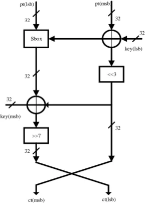
The Fig.1 shows that, from the 64-bits of the plaintext, 32-bits from the MSB are inserted into the S-box to get the substituted values. These are XORed with the 32-bits from the LSB of the plaintext and 32-LSB bits of the round key. The values obtained are then circularly shifted to the left by three and then XORed with the substituted bits of the plaintext and the 32-MSB bits of the round-key. The result obtained is then circularly shifted to the right by seven. These set of operations are performed for 31 rounds to obtain the corresponding ciphertext.
Key Scheduling
The key scheduling is similar to that of PRESENT cipher. The key-scheduling in this cipher is resistant to popular attacks and quite robust in its performance [8]. For a given 128-bits key, the 64 LSB bits are utilized in the XOR operations with the plaintext.
For a given key,
Key = a127a126a125 ……a2a1a0
Sbox
<<3
>>7 pt(lsb)
ct(msb) ct(lsb)
32
32 32
32
32
32 32
pt(msb)
key(lsb)
[image:2.595.87.233.545.748.2]key(msb)
Fig 1. Encryption in LiCi cipher. Klsb = a31a30a29………....a2a1a0
The key is updated as,
1. Key <<< 13 (Circularly shifted to the left by 13-bits) 2. S [a3a2a1a0] [a3a2a1a0]
3. S [a7a6a5a4] [a3a2a1a0]
4. [a63a62a61a60a59] ⊕Roundcounteri[a63a62a61a60a59]
Here RoundCounterigives the value of the round counter, which is to be XORed with the 5-bits from the key-bits (a63to
a59).
III. PROPOSEDARCHITECTURES A. Serial Architecture
This architecture is motivated by the serial architecture for PRESENT cipher for low-area with high latency and low performance [16]. The Fig.2 shows the proposed serial architecture designed with an input datapath of 8-bits. The first 16 clock cycles are required for the loading of plaintext and the key. The plaintext bits need a total 8 clock cycles for loading. The MSB and LSB bits are loaded in separate registers of 32-bits to facilitate easy processing of the operations involved. The loading of the input plaintext bits is done with the help of 2:1 multiplexers and shift registers. For the key, the data is loaded serially in a shift register of 128 bits. This constitutes for the first state (S0) of the FSM as
shown in Fig.3 wherein, the data is loaded and stored and then moves to the next state after 16 clock cycles.
In the state S1, the first XOR operation is performed with
the LSB bits of the plaintext and the substituted MSB bits along with the LSB bits of the key. For proper selection of the required bits to be XORed at each step, decoding logic is needed which incurs additional hardware. On successful completion of the XOR operation, the 32-bits intermediate result is circularly shifted to the left by 3-bits and stored in the MSB register. This state requires 4 cycles for substitution and the XOR operation is performed concurrently with the arrival of the substituted bits.
The substitution is performed with the help of two S-boxes as opposed to the eight S-boxes used in the original design. The substituted bits also need to be stored as the XOR in the next state is dependent on the substituted bits. Hence, in an attempt to decrease the area overhead, the same register used for LSB bits is reused for this purpose. The first XOR operation and the circular left shift by 3-bits is complete at the end of the 4th cycle of the state S1. This result is stored in
the MSB register, which also serves as the MSB input of the next round.
In the state S2, the second XOR operation is performed
International Journal of Innovative Technology and Exploring Engineering (IJITEE) ISSN: 2278-3075,Volume-8 Issue-6, April 2019 In the stage S3, the key-scheduling is performed to
calculate the key for the next
Key (lsb)
Key (msb)
2:1
Reg2
<<3
KeyReg
>>7
Reg1
Sbox
>>13 2:1
2:1 2:1
2:1
ld 8
8
8 pt
(lsb) pt
(msb)
8
64 rc
5
51 128
8 8
8 8
[image:3.595.53.298.77.253.2]8
Fig 2. Proposed Serial Architecture.
S0 S1
S2 S3
count<=15
count==15
count<=3
count==3
count==3 count<=3 start
Fig 3. FSM for Proposed Serial Architecture.
round as per the operations in the algorithm. The S-box used for substituting the plaintext bits is reused in this state, for substituting the 8-bits of the key for the next round. This requires a single clock cycle.The next state depends on whether or not a new input is being loaded or the next round from a total of 31 rounds is to be executed. In all, for a single round, the number of clock cycles needed are 4 for first XOR operation, another 4 for the second XOR operation and a single clock cycle for the key scheduling. Hence, a total of 9 clock cycles for a single round. With the inclusion of 16 clock cycles for the loading, 9clock cycles for the data processing and key scheduling for 30rounds and 8 clock cycles for the 31st round, a total of 294 clock cycles are needed to obtain the first output. The 31st round needs a clock cycle less due to the fact that key scheduling isn't required for the next round. As can be observed, the latency has increased, maximum frequency decreases with reduction in the area due to the reuse of S-boxes and registers. However, additional area is also incurred for the design of FSM and a counter to control its states. Also, suitable comparators and decoders are also needed for proper routing of the desired bits. It is to be noted that the output ciphertext is obtained through a 64-bits port. If it is required to reduce port size, additional registers would be needed to hold the MSB part of the cipher till the LSB part is calculated. In addition, a decoder would be necessary to output the bits in 8 clock cycles. However, this was not considered in the design proposed.
The design of serial architectures for Feistel networks is not as straight-forward as that of an SPN like PRESENT due to the non-uniform logic for the LSB and MSB sections [16]. Hence, the design should be such that the common logic for the MSB and LSB parts can be reused to incur less area.
ROM for Key Reg1
Sbox Reg2
>>7 <<3 2:1
2:1 Key(lsb)
Key(msb) 32
Key(lsb)
Key(msb)
Fig 4. Proposed Reduced Datapath Architecture.
S0 S1
S2
next
wait ld !ld
ld
Fig 5. FSM for Proposed Reduced Datapath Architecture.
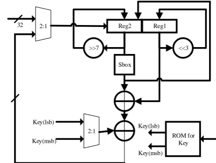
B. Reduced Datapath Architecture
[image:3.595.312.533.112.278.2]As per the proposed design, the initial loading requires 2 clock cycles by considering 32-bits data input at a time. The 32-bits of the LSB and the substituted segments of the MSB bits are stored in different registers. The substitution is done by the eight S-boxes as per the original algorithm. This accounts for the first state S0 as can be observed in the FSM
states shown in Fig.5
In the next state S1, the first XOR operation is performed in
one clock cycle with the stored LSB bits, substituted bits of the MSB part and the LSB key values from the ROM-module. The key values are selected from the ROM-module based on the control signals generated in the intermediate states. This XORed result is circularly shifted to the left by three and stored in the LSB register for reuse in the next state. In the following state S2,the second XOR
operation is performed with the stored substituted value, the result of the circular left shift by three bits in the LSB register and the MSB key values from the ROM- module. This XORed result is then circularly shifted to the right by seven bits and stored in the MSB register. The next state depends on whether a new input is being loaded or the next round from a total of 31 rounds is to be computed. Each round requires 2 clock cycles. Hence, the loading requires 2 clock cycles and for processing of all the rounds, 62 clock cycles are required. In all, 64 clock cycles are needed if a 64- bit output is considered as the ciphertext.
If the datapath width of the ciphertext is also to be reduced, another state for the proper rearrangement of the LSB and MSB segments are needed along with a decoding logic for proper direction of the ciphertext bits. In this design, the output considered was of 64-bits and simple wiring of the LSB and MSB parts was done to reduce the area consumption.
C. Pipeline Architecture
The Fig.6 shows the proposed pipelined hardware architecture for LiCi cipher. It was designed in an attempt to pipeline the round-based architecture. Although the latency is high in a round-based architecture, the area requirements are minimum as the same structure can be reused multiple times depending on the number of rounds required for encryption. The latency increases due to the dependence of the input of the next round on the output of the previous round.
In this design, the maximum operating frequency improves at the expense of larger area due to the additional registers required to store the intermediate results. The traditional round-based architecture can be designed without the intermediateregisters as there is no overlapped execution as
2:1
Sbox
2:1 2:1
Sbox 64
5 51 8 5
key(msb)
Shl<<3
Shr>>7
Shl<<13
ct(lsb) pt(msb) pt(lsb) key
128
32
32 key(lsb)
32 32
32 32
Fig 6. Proposed Pipelined Architecture.
in a pipelined design.
A complete loop-unrolled design is the easiest way to pipeline with the inclusion of intermediate registers at the end of each round. This consists of cascading all the XORs, S-boxes as many times as the number of rounds which results in a huge area and power consumption with high throughput [15]. However, it is unrealistic to categorize such a design under the lightweight domain.
In the Fig.6, it can be observed that the 64-bits input plaintext is separately routed through 32-bits 2:1 multiplexer and the input key through 128-bits 2:1 multiplexer. In the first stage, the LSB bits of the plaintext and the substituted values of the MSB bits are stored along with the 32 LSB bits of the key. These values are XORed and shifted to the left by 3-bits and stored in the intermediate registers on the next clock cycle. Concurrently, the previously substituted values in the first stage and the MSB bits of the key are passed through intermediate registers to calculate the XOR for the second stage and shifting the result circularly to the right by 7-bits. The previously shifted result of 3-bits from the previous stage and the result from the second stage account for the input of the next stage. The ciphertext results for the two inputs are obtained one after the other on successful completion of all the rounds.
As can be observed, due to the stagewise division of the combinational path, there is a possibility for the acceptance of a second input even before the first ciphertext is obtained. This is not feasible in the case of traditionalround-based architecture.However, due to the processing of dual inputs in a round-based structure, as opposed to a single input, thelatency is nearly double.
International Journal of Innovative Technology and Exploring Engineering (IJITEE) ISSN: 2278-3075,Volume-8 Issue-6, April 2019 It is to be noted that the results are not as enhanced as
expected in the case of SPNs. This is due to the variation in the data processing of the input plaintext which is dependent on the interchanging of the results from the previous stage. As a result, the MSB bits of the output need to be stored until the LSB bits are obtained which require additional registers to store the results.
IV. HARDWARECOMPARISON
The area consumption for a hardware design is measured interms of gate equivalents in ASIC implementations. However, in recent years, FPGAs have gained importance due to their short lifetime to market and reconfigurable nature.The designs under evaluation in Table I and Table II are referred as
1)Serial Architecture (S)
2)Reduced Datapath Architecture (Rd) 3)Pipelined Architecture (P)
The architectures were implemented at Register Transfer Level using Verilog. The results were tabulated for the implementation usingPost Place and Route option in Xilinx ISE 14.6. Further, the simulations were observed in ISim Simulator for an input stimulus. The power analysis was performed in Xilinx Power Analyzer (XPA) which is a part ofXilinx ISE. The other synthesis options were the default options set.The area consumption in an FPGA is usually discussed with regards to number of slices occupied. The performance can be estimated based on latency and throughput.Power
consumption by and large depends on the algorithm used, clock frequency, threshold voltage and the technology usedforimplementation.The dynamic power consumption is due tochange in the content of the flip flops due to clock transitions [20].
[image:5.595.98.504.299.620.2]The results for the architectures proposed are evaluated for
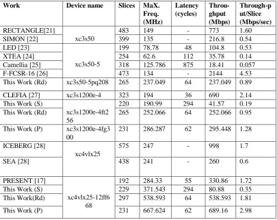
Table I: Hardware comparison of the proposed architectures with existing ciphers.
Work Device name Slices MaX.
Freq. (MHz)
Latency (cycles)
Throu-ghput (Mbps)
Through-p ut/Slice (Mbps/sec) RECTANGLE[21]
xc3s50
483 149 - 773 1.60
SIMON [22] 399 135 - 216.8 0.54
LED [23]
xc3s50-5
199 78.78 48 104.8 0.53
XTEA [24] 254 62.6 112 35.78 0.14
Camellia [25] 318 125.786 875 18.41 0.057
F-FCSR-16 [26] 473 134 - 2144 4.53
This Work (Rd) xc3s50-5pq208 265 237.049 64 237.049 0.89
CLEFIA [27] xc3s1200e-4 323 194 36 690 2.14
This Work (S)
xc3s1200e-4ft2 56
220 190.99 294 41.57 0.19
This Work (Rd) 265 252.066 64 252.066 0.95
This Work (P) xc3s1200e-4fg3 00
231 286.287 62 295.448 1.28
ICEBERG [28]
xc4vlx25
575 247 - 998 1.7
SEA [28] 438 241 - 260 0.6
PRESENT [17]
xc4vlx25-12ff6 68
192 284.33 55 330.86 1.72
This Work (S) 229 371.543 294 80.88 0.35
This Work(Rd) 297 538.593 64 538.593 1.81
Fig 7. Resource usage comparison of the proposed architectures.
Fig 8. Throughput per Slice comparison of the proposed architectures.
Table II. Comparison of Dynamic Power Consumption in milliwatts with previous results.
WORK DYNAMIC POWER
CONSUMPTION IN MILLI WATTS
LED[13] 100
PRESENT[13] 38
SPECK[13] 35
RECTANGLE[13] 31
LICI[13] 30
PICO[29] 28
THIS WORK(P) 27.86
THIS WORK (S) 15.19
THIS WORK(RD) 0.98
Xilinx FPGA series.The focus is on the Spartan 3 seriesand Virtex 4 series for faircomparison with the results from the existing ciphers.
V.DISCUSSIONOFRESULTS
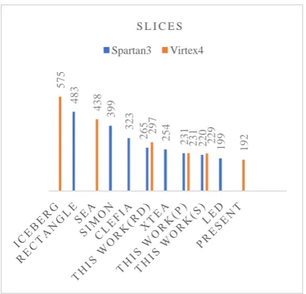
[image:6.595.75.270.309.500.2]The Fig.7 shows the resource usage comparison in terms of slices for Virtex 4 and Spartan 3 families. The proposed architectures occupy lesser area compared to most ciphers. However, they can be further optimized for lesser area to compete with SPNs like PRESENT and LED. The Fig.8 gives the throughput/slice comparison with the existing ciphers. It can be observed that among the three proposed architectures, the pipelined architecture has the best performance and operating frequency and the serial architecture has the least performance due to increased latency. The enhanced performance in the case of pipelined architecture can be attributed to the reduction in the critical path delay. The throughput per slice for the proposed architectures is found to be better than the popular ciphers like PRESENT and LED. The Fig.9 shows the dynamic power consumption results calculated in XPower Analyzer for a clock frequency of 10 MHz on Virtex 6 platform, the same family used by the authors in the base paper[13]. The proposed architectures were evaluated for xc6vlx75-3ff784. It can be illustrated from the results that the dynamic power consumption is very low in the case of reduced datapath.design. The pipelined architecture has more dynamic power consumption due to the
Fig 9. Illustration ofDynamic Power consumption comparison with the previous results.
483
399
323
265 254 231 220
199
575
438
297
231 229
192
S L I C E S
Spartan3 Virtex4
100
38 35 31 30 28 27
.8
6
1
5
.1
9
0
.9
8
D Y N A M I C P O W E R I N M I L L I W A T T S
[image:6.595.319.540.528.684.2]International Journal of Innovative Technology and Exploring Engineering (IJITEE) ISSN: 2278-3075,Volume-8 Issue-6, April 2019 increase in the number of registers. However, the dynamic
power consumption is lower than the other ciphers used for comparison.
It was found that the area consumption is least in the serial architecture. From Fig.9, it is observed that the dynamic power consumption of the pipelined architecture is higher compared to the other two proposed architectures at 10MHz frequency due to the intermediate registers involved. Nonetheless, it is lower than the remaining ciphers.
VI. CONCLUSION
In this paper, three different hardware architectures for the LiCi cipher are proposed. Choosing different constraints, a serial architecture, a reduced datapath architecture and a pipelined architecture are designed. The design strategy for the serial architecture is based on low area and power with serial processing of the input plaintext and key bits with tradeoffs in high latency and low performance. The reduced datapath architecture consists of reduction in the datapath width of the plain-text bits with a ROM based key-scheduling. This is designed choosing tradeoffs from security, moderate latency for low-area and minimal power. The pipelined architecture is designed for high performance with moderate area and moderate latency by reducing the critical path delay. The designs are implemented for FPGA boards like Spartan 3, Virtex 4 and Virtex 6.The area overhead is compared in terms of slices with the existing ciphers. Further, the latency and the maximum frequency obtained from the synthesized results is used to calculate the throughput and throughput per slice which gives an estimate of the performance. The power consumption is discussed in terms of dynamic power consumption at 10MHz clock frequency. There is further scope to enhance the results in terms of area or speed by utilizing the existing resources of FPGA like BRAM, SRL16 using efficient encoding schemes for the FSMs with implementation in RAM/ROM [30]. The usage of BRAM blocks in FPGAs can reduce the slice count with a reduction in speed. It can be concluded that the proposed architectures are well-suited for low-area and low-power applications based on moderate security. The tradeoffs must be chosen from area, power, throughput and latency thus making the architectures application specific.
REFERENCES
1. Silva, Bhagya Nathali, Murad Khan, and Kijun Han. "Internet of things:
A comprehensive review of enabling technologies, architecture, and challenges." IETE Technical Review. Vol 35, no. 2,pp. 205-220,2018.
2. Cooper, Joshua, and Anne James. "Challenges for database
management in the internet of things." IETE Technical Review vol.26, no. 5 ,pp. 320-329,2009.
3. J.H. Kong, L. M. Ang, and K.P. Seng, "A comprehensive survey of
modern symmetric cryptographic solutions for resource-constrained environments," Journal of Network and Computer Applications, vol. 49, pp. 15-50, 2015.
4. Poschmann, Axel York. "Lightweight cryptography: cryptographic
engineering for a pervasive world." In PH. D. THESIS. 2009..
5. K. A. McKay, L. Bassham, M. S. Turan, and N. Mouha, Report on
lightweight cryptography: US Department of Commerce, National Institute of Standards and Technology, 2017.
6. T.Eisenbarth, S. Kumar, C. Paar, A. Poschmann, and L. Uhsadel, "A
survey of lightweight-cryptography implementations," IEEE Design & Test of Computers, pp. 522-533, 2007
7. DeeptiSehrawat and Nasib S. Gill. “Lightweight Block Ciphers for IoT
based applications : A Review.” International Journal of Applied Engineering Research, vol.13, no.5, pp. 2258-2270,2018.
8. A. Bogdanov, L. R. Knudsen, G. Leander, C. Paar, A. Poschmann, M. J.
Robshaw, Y. Seurin, and C. Vikkelsoe, "PRESENT: An
ultra-lightweight block cipher," in International Workshop on Cryptographic Hardware and Embedded Systems, 2007, pp. 450-466.
9. J. Guo, T. Peyrin, A. Poschmann, and M. Robshaw, “The LED block
cipher,” Lecture Notes in Computer Science (including subseries Lecture Notes in Artificial Intelligence and Lecture Notes in Bioinformatics): Preface, vol. 6917, pp. 326–341, 2011.
10.National Institute of Standards and Technology. FIPS 197: Advanced
Encryption Standard. Available via
https://csrc.nist.gov/publications/fips/, 12. March 2019.
11.Z. Xiang, W. Zhang, Z. Bao, and D. Lin, "RECTANGLE: a bit-slice
lightweight block cipher suitable for multiple platforms," Science China Information Sciences, vol. 58, pp. 1-15, 2015.
12.K. Shibutani, T. Isobe, H. Hiwatari, A. Mitsuda, T. Akishita, and T.
Shirai, "Piccolo: an ultra-lightweight blockcipher," in International Workshop on Cryptographic Hardware and Embedded Systems, 2011, pp. 342-357.
13.J. Patil, G. Bansod, and K. S. Kant, "LiCi: A new ultra-lightweight
block cipher," in Emerging Trends & Innovation in ICT (ICEI), 2017 International Conference on, 2017, pp. 40-45.
14.R. Beaulieu, S. Treatman-Clark, D. Shors, B. Weeks, J. Smith, and L.
Wingers, "The SIMON and SPECK lightweight block ciphers," in Design Automation Conference (DAC), 2015 52nd ACM/EDAC/IEEE, 2015, pp. 1-6.
15.Rolfes, Carsten, Axel Poschmann, Gregor Leander, and Christof Paar.
"Ultra-lightweight implementations for smart devices–security for 1000 gate equivalents." In International Conference on Smart Card Research and Advanced Applications, pp. 89-103. Springer, Berlin, Heidelberg, 2008.
16.Hanley, Neil, and Maire ONeill. "Hardware comparison of the ISO/IEC
29192-2 block ciphers." In 2012 IEEE Computer Society Annual Symposium on VLSI, pp. 57-62. IEEE, 2012.
17.C. A. Lara-Nino, A. Diaz-Perez, and M. Morales-Sandoval,
"Lightweight hardware architectures for the PRESENT cipher in FPGA," IEEE Transactions on Circuits and Systems I: Regular Papers, vol. 64, pp. 2544-2555, 2017.
18.C. A. Lara-Nino, M. Morales-Sandoval, and A. Diaz-Perez, “Novel
FPGA-based low-cost hardware architecture for the PRESENT block cipher,” in Proc. Euromicro Conf. Digit. Syst. Design, Aug./Sep. 2016,pp. 646–650.
19.A. Moradi, A. Barenghi, T. Kasper, and C. Paar, “On the vulnerability
of FPGA bitstream encryption against power analysis attacks: Extracting keys from Xilinx Virtex-II FPGAs,” in Proc. 18th ACM Conf. Comput. Commun. Secur. (CCS), New York, NY, USA, 2011, pp. 111–124.
20.Xilinx Inc. Virter-4 FPGA User Guide, March,2019. Available at:.
https://www.xilinx.com/support/documentation/user_guides/ug070.pdf .
21.S. Feizi, A. Nemati, A. Ahmadi and V. A. Makki, "A high-speed FPGA
implementation of a Bit-slice Ultra-Lightweight block cipher, RECTANGLE," 2015 5th International Conference on Computer and Knowledge Engineering (ICCKE), pp. 206-211. Mashhad, 2015.
22.A.Aysu, E. Gulcan and P. Schaumont, "SIMON Says: Break Area
Records of Block Ciphers on FPGAs," in IEEE Embedded Systems Letters, vol. 6, no. 2, pp. 37-40. June 2014.
23.Anandakumar, N. Nalla, Thomas Peyrin, and Axel Poschmann. "A very
compact FPGA implementation of LED and PHOTON." International Conference in Cryptology in India. pp.304-321. Springer, Cham, 2014.
24.J. P. Kaps, "Chai-tea, cryptographic hardware implementations of
xtea,"INDOCRYPT 2008, Lecture Notes in Computer Science, vol. 5365,pp. 363-375. Springer, 2008.
25.P.Yalla and J.-P. Kaps, “Compact FPGA implementation of Camellia,”
in FPL 2009, M. Danˇek, J. Kadlec, and B. Nelson, Eds. IEEE, Aug. 2009, pp. 658–661.
26.D. Hwang, M. Chaney, S. Karanam, N. Ton, and K. Gaj, “Comparison
of FPGA-targeted hardware implementations of eSTREAM stream cipher candidates,” in Proc. State of the Art of Stream Ciphers Workshop, SASC 2008 , Lausanne, Switzerland, Feb 2008, pp. 151–162.
27.P.Proenca and R. Chaves, "Compact CLEFIA Implementation on
28.F. Mace, F. -. Standaert and J. -. Quisquater, "FPGA Implementation(s) of a Scalable Encryption Algorithm," in IEEE Transactions on Very Large Scale Integration (VLSI) Systems, vol. 16, no. 2, pp. 212-216. Feb. 2008.
29.Bansod, Gaurav, Narayan Pisharoty, and Abhijit Patil. "PICO: an ultra
lightweight and low power encryption design for ubiquitous computing." Defence Science Journal 66, no. 3, pp.259-265.2016.
30.P.Yalla and J. Kaps, "Lightweight Cryptography for FPGAs," 2009
International Conference on Reconfigurable Computing and FPGAs, Quintana Roo, 2009, pp. 225-230.
AUTHORSPROFILE
Nigar Ayeshais currently pursing M.Tech. in VLSI and
Embedded Systems from National Institute of
Technology, Raipur. Her research interests include hardware implementation and optimization of Lightweight
Cryptographic ciphers for resource constrained
environments, Digital System Design and Verification, VLSI System Design.
Bibhudendra Acharyareceived the M.Tech. and Ph.D.
degree in Electronics and Telecommunication from National Institute of Technology, Rourkela, India. He is currently the Head and Assistant Professor in the
Electronics and Telecommunication Engineering