Polyimide Film
Jacob Solomon Hughes
A thesis submitted for the degree of Doctor of Philosophy of
The Australian National University
December, 2018
c
Copyright by Jacob Solomon Hughes 2018
This thesis is an account of research undertaken between February 2013 and December
2018 at The Research School of Physics and Engineering, College of Physical and
Mathe-matical Sciences, The Australian National University, Canberra, Australia. Except where
acknowledged in the customary manner, the material presented in this thesis is, to the
best of my knowledge, original and has not been submitted in whole or part for a degree
in any university.
A Ph. D. is a gigantic undertaking and there are many people that I would like to
ac-knowledge and express my heartfelt thanks to.
Firstly, I would like to thank James Sullivan, my primary supervisor, the chair of my
supervisory committee, and the leader of the Positron Group at ANU. James’ direction
and support were paramount in the undertaking this work.
I would like to thank David Sprouster, who provided expertise in materials science and
helped design the experimental programme for this work, as well as great mentoring and
guidance.
I would like to thank Stephen Buckman not only for his role on my supervisory
com-mittee, but additionally for his role as a teacher in the Honours programme in the year
before I began my Ph. D.
I would like to acknowledge and thank the members of the positron group at the
Aus-tralian National University (in no particular order): Tamara Babij, Daniel Murtagh, Colin
Campbell, David Stevens, Simon Armitage, and Josh Mahacek. Ross Tranter and Stephen
Battison, the technical staff, were invaluable help and a continual source of support.
Cormac Corr and Sam Cousens from the Department of Plasma Physics helped with
the use of MAGPIE and generously spent a lot of their own time babysitting me and the
Kapton samples I was exposing to plasma.
Johannes Postler helped kick start all of the digital measurement efforts.
Gregory Lane at the Department of Nuclear Physics provided me with great advice in
spectroscopy and HPGe detectors.
Finally, my thanks go to the espresso machine in the positron laboratory, that is to
this day the hardest working member of the positron group. The laboratory and group
members would surely fall to ruin without the daily support of this under-appreciated
paragon of caffeinated beverages.
Studying and understanding the internal structure of materials is important to
develop-ment of device quality materials with well-defined electrical and mechanical properties.
More and more, modern materials for highly optimised applications are manufactured
material composites, or processed in some way. To understand macroscopic properties
exhibited by these materials often atomic or nano scale changes need to be characterised
and understood, as they can be the drivers for these effects.
Positron annihilation spectroscopy (PAS) is an established analytical technique used
to investigate the internal structure of materials, as the different techniques are
non-destructive and sensitive at the molecular (sub-nanometre) level. Developing high quality
positron spectroscopy experiments can aid in the understanding of the evolution of
mate-rials over time in damaging environments, or precisely monitor material behaviour during
fabrication and processing. The information obtained from PAS can identify the
un-derlying causes of desirable macroscopic material properties and inform the design and
manufacture of these materials for better performance.
At the Australian National University, the positron research group has developed
positron annihilation lifetime spectroscopy (PALS) which relates the time taken for an
im-planted positron to annihilate inside a material to defect size and concentration. This
the-sis outlines the implementation of a complementary PAS technique added to the positron
materials beamline, Doppler broadening of annihilation radiation (DBAR), which provides
additional information on the chemical environment at positron annihilation sites.
The successful implementation of the DBAR experiment was used to characterise ion
implanted and plasma exposed Kapton polyimide, in conjunction with existing positron
techniques. The damage study explored the effects of damage similar to
environmen-tal exposure in long term space missions, where Kapton components from satellites or
spacecraft interact with trapped ion plasmas inside the Earth’s magnetic field, planetary
atmospheres, and the solar wind.
Declaration iv
Acknowledgments vi
Abstract viii
Contents ix
List of Figures xiii
1 Introduction 1
1.1 Characterisation of Materials . . . 2
2 Positron Annihilation Spectroscopy 5 2.1 The Positron . . . 5
2.1.1 Positron Annihilation . . . 7
2.1.2 Positronium . . . 9
2.2 Positron Sources for Experiments . . . 11
2.2.1 Reducing Positron Energy . . . 13
2.3 Positron Interactions with Matter . . . 14
2.3.1 Implantation of Positrons into Solid Materials . . . 16
2.4 Positron Annihilation Lifetime Spectroscopy . . . 17
2.4.1 PALS Data . . . 18
2.4.2 Bulk PALS Systems . . . 19
2.4.3 Pulsed Beam PALS . . . 20
2.4.4 Resolution of Lifetimes . . . 21
2.4.5 The Tao-Eldrup Model . . . 21
2.5 Doppler Broadening of Annihilation Radiation . . . 22
2.5.1 Doppler Broadening in Positron Spectroscopy . . . 22
2.5.2 The S Parameter Measurement . . . 23
2.5.3 The W Parameter Measurement . . . 25
2.5.4 Information From DBAR Measurements . . . 26
2.6 Other Positron Techniques . . . 28
2.6.1 Reflection High-Energy Positron Diffraction . . . 28
2.6.2 Angular Correlation of Annihilation Radiation . . . 28
2.6.3 Age-Momentum Correlation . . . 28
3 Positron Annihilation Lifetime Spectroscopy at ANU 31 3.1 Overview of the PALS Experiment . . . 31
3.2 Experimental Set-up . . . 32
3.2.1 Source Stage and Primary Beam . . . 32
3.2.2 Trap Stage . . . 37
3.2.3 Sample Stage . . . 42
3.3 Typical Operating Parameters . . . 44
3.4 Preliminary Estimation and Simulation . . . 44
3.5 Data Analysis . . . 46
4 Development of a Doppler Broadening Spectroscopy Experiment 49 4.1 Motivation . . . 49
4.2 Positron Materials Beamline for DBAR Experiments . . . 50
4.3 High Purity Germanium Detectors . . . 51
4.3.1 Coaxial Standard Electrode HPGe Detector . . . 51
4.3.2 Detector Pre-Amplifier . . . 52
4.3.3 Detector Cooling System . . . 52
4.4 Initial Resolution Benchmark . . . 53
4.4.1 Manufacturer’s Calibration . . . 53
4.4.2 Experimental Set-up . . . 54
4.4.3 Calibrated results . . . 55
4.4.4 Conclusion . . . 56
4.5 Full Digital DBAR System . . . 56
4.5.1 Motivation for a fully digital DBAR system . . . 57
4.5.2 Experimental Set-up . . . 57
4.5.3 Digitiser Resolution . . . 59
4.5.4 Data Analysis . . . 60
4.5.5 Waveform Fitting . . . 60
4.5.6 Digital Results . . . 64
4.5.7 Investigating R2 adj . . . 66
4.5.8 Investigatingχ2 . . . 68
4.5.9 Digital Fitting Resolution . . . 69
4.5.10 Conclusion . . . 70
4.6 Digital Filtering . . . 70
4.6.1 Experimental Set-up . . . 70
4.6.2 Digital Filtering Results . . . 72
4.7 Analogue DBAR System . . . 76
4.7.1 Experimental Set-up . . . 76
4.7.2 Detector Efficiency . . . 77
4.7.3 Analogue Resolution Measurement . . . 80
4.7.4 Calibration Results . . . 81
4.8 Spectrum Post-Processing . . . 82
4.8.1 Experimental Set-up . . . 83
4.8.2 Post-Processing Method . . . 83
4.8.3 Post-Processing Results . . . 85
4.9 Conclusion . . . 85
5 Elemental Specificity using DBAR 89 5.1 Method . . . 89
5.1.1 Sample Measurement . . . 89
5.1.2 Treatment of data . . . 90
5.1.3 Details of Measured Materials . . . 92
5.2 Basic Metals . . . 94
5.3 Transition Metals . . . 96
5.3.1 Row 4 Transition Metals . . . 96
5.3.2 Group 6 Transition Metals . . . 98
5.3.3 Group 11 Transition Metals . . . 99
5.4 Semiconductors . . . 100
5.5 Organic Materials . . . 102
5.6 Discussion . . . 105
6 Experiments with Kapton Polyimide 109 6.1 Properties and Applications of Kapton . . . 109
6.2 Manipulating the Properties of Kapton . . . 110
6.3 Plasma Damage in Kapton . . . 111
6.4 The Space Environment . . . 111
6.4.1 The van Allen Radiation Belts . . . 112
6.4.2 The Solar Wind . . . 112
6.5 Recreating Space-like Conditions in the Laboratory . . . 113
6.6 Experimental Programme for Ion Damaged Kapton . . . 115
7 Ion Implantation into Kapton Polyimide Film 117 7.1 Sample Preparation and Experimental Set-up . . . 117
7.2 300keV Gallium Implantation . . . 120
7.2.1 Near Surface Region . . . 120
7.3 50keV Oxygen Implantation . . . 122
7.3.1 50keV Oxygen Implantation at Low Fluence . . . 122
7.3.2 50keV Oxygen Implantation at High Fluence . . . 127
7.4 100keV Oxygen Implantation . . . 131
7.4.1 100keV Oxygen Implantation at High Fluence . . . 131
7.5 Discussion . . . 133
8 Plasma Interaction with Kapton Polyimide Film 141 8.1 Sample Preparation and Experimental Set-up . . . 141
8.2 Plasma Exposed Kapton . . . 142
8.3 50keV Implanted Oxygen and Plasma Exposure . . . 142
8.4 100keV Implanted Oxygen and Plasma Exposure . . . 147
8.5 Discussion . . . 150
9 Conclusion 157 9.1 DBAR Experiment . . . 157
9.2 Space Relevant Damage in Kapton Polyimide Film . . . 158
9.2.1 Ion Implantation into Kapton Polyimide Film . . . 159
9.2.2 Plasma Interaction with Kapton Polyimide Film . . . 160
9.3 Future Work . . . 161
9.3.1 Positron Materials Beamline . . . 162
9.3.2 Expanded Characterisation of Damaged Kapton . . . 162
A Appendix A: Calibration data for the DBAR system 167 A.1 Efficiency and Resolution Calibration . . . 167
2.1 Feynman diagrams of positron-electron annihilation . . . 7
2.2 Feynman diagrams of less probable positron-electron annihilation . . . 8
2.3 22Na decay scheme . . . . 11
2.4 Distribution of emitted positron energy from22Na . . . . 11
2.5 Cartoon of positron interactions with matter . . . 15
2.6 Makhov implantation profiles of various energy for aluminium . . . 17
2.7 Example PALS spectra analysing as-grown and irradiated silicon . . . 19
2.8 The Tao-Eldrup model . . . 21
2.9 S parameter measurement region . . . 24
2.10 W parameter measurement region . . . 25
2.11 S parameter depth profile plot of germanium implanted as-grown crystalline germanium . . 27
3.1 Schematic of the entire beamline . . . 33
3.2 Schematic of source stage . . . 34
3.3 Typical grow curve for a solid neon RGS moderator . . . 36
3.4 Schematic of the Surko buffer gas trap . . . 37
3.5 Electrode potentials in the trap . . . 38
3.6 Electrode potentials in the trap cycle . . . 39
3.7 Tuning the positron pulse FWHM as a function of final electrode potential . . . 40
3.8 The time varying potential applied to electrode 8 . . . 41
3.9 Schematic of the sample stage . . . 42
3.10 Example simulated implantation of 300keV gallium ions into Kapton . . . 45
3.11 pyPenelope simulation of positron implanted OLED . . . 46
4.1 Typical absolute efficiency for coaxial Ge crystal . . . 54
4.2 Results of initial calibration . . . 55
4.3 Block diagram of full digital setup . . . 58
4.4 Example pre-amplifier waveform . . . 58
4.5 Example of digital data and fit . . . 63
4.6 Full fitting of the rising edge of the pre-amplifier waveform . . . 63
4.7 Detailed view of the waveform rising edge . . . 63
4.8 Parameter search to improve the resolution in137Cs . . . . 64
4.9 Spectrum of152Eu collected with the full digital experimental . . . . 65
4.10 Spectrum of137Cs collected with the full digital experimental . . . . 65
4.11 Histogram of R2 adj values from the spectrum of 152 Eu . . . 67
4.12 R2 adj discriminated spectrum of 152 Eu . . . 67
4.13 Histogram ofχ2 values . . . 68
4.14 χ2 spectrum of152Eu . . . 69
4.15 Comparison of digital and initial test resolution . . . 69
4.16 Digital filter frequency response . . . 71
4.17 Comparison of raw and filtered waveforms . . . 71
4.18 Direct comparison of the raw and digitally filtered pre-amplifier waveforms . . . 72
4.19 Comparison of the results of fitting the raw and filtered data . . . 73
4.20 Spectrum of152 Eu collected using the digitally filtered waveforms . . . 74
4.21 Effective resolution of digital filter compared to MCA data . . . 75
4.22 Block diagram of the analogue data collection stage of the DBAR experiment. . . 76
4.23 Normalised efficiency at 15cm . . . 79
4.24 Detector resolution at 15cm . . . 80
4.25 Final adjusted spectrum of152 Eu . . . 81
4.26 Final adjusted spectrum of137 Cs . . . 81
4.27 Investigation of laboratory background radiation environment . . . 82
4.28 Example DBAR spectra post-processing of c-Al . . . 84
5.1 Examination of uncertainty in ratio measurements . . . 91
5.2 Momentum broadening spectrum of basic metals . . . 95
5.3 Momentum broadening spectrum of basic metals in ratio to aluminium . . . 95
5.4 Momentum broadening spectrum of row 4 transitions metals . . . 97
5.5 Momentum broadening spectrum of row 4 transition metals in ratio to aluminium . . . 97
5.6 Momentum broadening spectrum of group 6 transitions metals . . . 98
5.7 Momentum broadening spectrum of group 6 transition metals in ratio to aluminium . . . . 98
5.8 Momentum broadening spectrum of group 11 transitions metals . . . 99
5.9 Momentum broadening spectrum of group 11 transition metals in ratio to aluminium . . . . 99
5.10 Momentum broadening spectrum of semiconductor elements . . . 101
5.11 Momentum broadening spectrum of semiconductor elements in ratio to aluminium . . . 101
5.12 Momentum broadening spectrum of organic materials . . . 104
5.13 Momentum broadening spectrum of organic materials in ratio to aluminium . . . 104
5.14 Comparison of elemental specificity by Asoka-Kumaret al. . . . . 106
5.15 Comparison of elemental samples measured by Asoka-Kumar . . . 106
6.1 Chemical structure of a single Kapton polyimide molecule . . . 109
7.1 Simulated implantation of 50keV oxygen ions into Kapton . . . 119
7.3 Simulated implantation of 300keV gallium ions into Kapton . . . 119
7.4 Near-surface momentum distribution of Kapton: 50keV oxygen at low fluence . . . 124
7.5 Maximum damage region momentum distribution of Kapton: 50keV oxygen at low fluence . 124
7.6 S parameter depth profile of Kapton: 50keV oxygen at 1×10¹⁴ ions·cm−2 . . . . 126
7.7 W parameter depth profile of Kapton: 50keV oxygen at 1×10¹⁴ions·cm−2 . . . . 126
7.8 Near surface momentum distribution of Kapton: 50keV oxygen at high fluence . . . 128
7.9 Maximum damage region momentum distribution of Kapton: 50keV oxygen at high fluence 128
7.10 S parameter depth profile of Kapton: 50keV oxygen at 1×10¹⁵ ions·cm−2 . . . . 130
7.11 W parameter depth profile of Kapton: 50keV oxygen at 1×10¹⁵ions·cm−2 . . . . 130
7.12 Near surface momentum distribution of 100keV oxygen implanted Kapton . . . 132
7.13 Maximum damage region momentum distribution of 100keV oxygen implanted Kapton . . . 132
7.14 S parameter depth profile of Kapton: 100keV oxygen at 1×10¹⁵ ions·cm−2 . . . . 134
7.15 W parameter depth profile of Kapton: 100keV oxygen at 1×10¹⁵ions·cm−2 . . . . 134
8.1 Near surface momentum distribution of plasma exposed Kapton implanted with 50keV oxygen144
8.2 Maximum damage region momentum distribution of plasma exposed Kapton implanted with
50keV oxygen . . . 145
8.3 S parameter depth profile of plasma exposed Kapton: 50keV oxygen at 1×10¹⁵ions·cm−2 145
8.4 W parameter depth profile of plasma exposed Kapton: 50keV oxygen at 1×10¹⁵ions·cm−2 146
8.5 Near surface momentum distribution of plasma exposed Kapton implanted with 100keV
oxygen . . . 148
8.6 Maximum damage region momentum distribution of plasma exposed Kapton implanted with
100keV oxygen . . . 149
8.7 S parameter depth profile of plasma exposed Kapton: 100keV oxygen at 1×10¹⁵ions·cm−2 149
8.8 W parameter depth profile of plasma exposed Kapton: 100keV oxygen at 1×10¹⁵ions·cm−2150
A.1 Efficiency at 7cm . . . 170
Introduction
The body of work presented in this thesis has been divided into two main sections. Firstly,
this work covers the design, implementation, and characterisation of a positron
annihila-tion spectroscopy experiment added to the established positron materials beamline in the
positron group at the Australian National University. Secondly, the suite of positron
an-nihilation spectroscopy measurements are used to characterise Kapton, a polyimide used
in spacecraft shielding, that has been damaged by ion implantation and plasma exposure,
in a manner related to the environmental conditions that are found in our solar system
and likely satellite orbit paths.
The positron materials beamline at the Australian National University makes use of the
positron annihilation lifetime spectroscopy technique (PALS), which correlates the lifetime
of a positron implanted into a material to the internal structure of that particular material.
The implanted positrons are sensitive to damage to the material in the form of vacancies,
pores, and voids, however a single measurement requires several hours to complete. The
additional experimental technique to be implemented examines the Doppler broadening
of annihilation radiation (DBAR), which measures the momentum of annihilation
pho-tons within material targets. By implementing the DBAR technique a complementary
and supportive measurement can be made in significantly less time, which augments the
information gained from the existing positron annihilation lifetime spectroscopy technique
already in use.
Following the implementation and characterisation of the Doppler broadening of
anni-hilation radiation technique, the experiment will be used to characterise Kapton polyimide
samples relevant to spacecraft applications. The polyimide samples, which are used for
thermal and electrical insulation in spacecraft, will be damaged to varying degrees by ion
implantation and exposure to plasma in a manner which relates to the type of damage
that could occur in the galactic environment or within atmosphere of a planet in the solar
system. The measurements aim to begin an investigation into not only the effects of ion
implantation at different preparation temperatures, but how any induced damage is
in-fluenced by exposure to plasma. The suite of conditions are designed to mimic the harsh
space environment that Kapton would be exposed to, while providing a set of experiments
that can characterise the damage found.
1.1
Characterisation of Materials
The manipulation of the electrical and mechanical properties of a material can be
per-formed by processing techniques that affect the base material at the molecular level, yet
still produce large scale changes. Well known examples of nanoscale material changes
that have important macroscopic effects are doped semiconductors. These materials are
extremely important for electronic devices, and are manufactured by introducing small
percentages of dopant species, which can dramatically change how these semiconductors
behave. Controlling the amount of dopants as a stoichiometric parameter will determine
whether these electrical properties manifest as desired: too little or too much and this
doped silicon will not function as desired and be useless.
Similarly to using dopants, using ions to damage a material can also change its
macro-scopic properties, as the implantation process damages the target material and
contam-inates the target with the implanted species. Careful control of the target material,
im-planted ion species, and implantation dose can transform the target material. An example
of this is the processing of organic polymer materials into molecular filters using ion
im-plantation.
Damage to materials can often be a slow process which builds up over time,
espe-cially when the damage is primarily from the environment in which the material operates.
In these cases chemical reactions can drive damage processes through exposed surfaces
interacting with the substances in the environment. Using high resolution techniques to
analyse these materials at different stages of environmental degradation, we can attempt to
determine which particular processes drive damage, as well as finding the likely outcomes
of this damage. The changes to specific properties can be characterised as a function of
The nanoscale changes that create macroscopic effects require a sensitivity of
mate-rial preparation and characterisation, and to be fully controlled the effects need to be
well understood. A key technique used for this type of study is positron annihilation
spectroscopy (PAS). PAS is a highly sensitive, high resolution, non-destructive technique
which is capable of sensing changes to materials at the atomic level.
Developing quality PAS experiments can help us to understand and improve material
Positron Annihilation
Spectroscopy
Positron annihilation spectroscopy (PAS) is a technique used in condensed matter and
materials physics studies to learn about the internal structure of a particular material.
The wider field of PAS is made up of several different experiment types, which each
exploit a particular facet of the physics surrounding positron annihilation in order to
reveal information about a sample.
To fully understand and interpret the information in the results of PAS techniques, it
is first important to understand the fundamental properties of the positron and mechanics
in positron-matter interaction.
This chapter will detail the physics involved in positron-matter interaction, in
partic-ular focusing in topics relevant to positron annihilation spectroscopy experiments. For
these positron spectroscopy techniques, the experimental method, data acquisition, and
data interpretation will be discussed, detailing the information obtained with each
tech-nique.
2.1
The Positron
The positron is the anti-particle counterpart to the electron and it is a charged lepton,
meaning it is an elementary particle with spin 1/2 which has a charge of +1e.
The discovery of the positron is relatively recent and the origins of the positron begin in
1929 with the publication of Dirac’s paperThe Quantum Theory of the Electron [1]. The
Dirac equation allowed for negative energy solutions, which could not be discarded due
to the quantum nature of the problem, unlike some negative energy solutions obtained
in classical mechanics. Early interpretations of these negative energy solutions caused
uncertainty in the scientific community at the time, and initially no-one had a universally
satisfactory explanation.
Throughout 1929 Dirac continued his work on these problems, with growing interest
and input from other physicists from around the world. Notably, at this time German
physicist Weyl attempted to reconcile gravitation and mass with the electromagnetic field,
using the Dirac equation, but failed [2]. The promising clue from his work points at these
“negative energy electrons” having the same mass as electrons. Dirac remained concerned
by the implications of his work so far. It appeared as though electrons could freely jump
from positive energy states to negative ones, which would have the effect of flipping their
charge, violating conservation of charge [3].
In 1930, Dirac suggests that the negative energy solutions could in fact be protons,
despite the huge difference in mass [4]. This suggestion is rebuked by Oppenheimer in a
letter, who comments that allowing protons and electrons to annihilate would make all
atoms very unstable, and since we observe a matter rich, stable universe, this cannot be
the case [5].
A new suggestion is put forward by Dirac in 1931 in the paperQuantised Singularities
in the Electromagnetic Field. Negative energy states must not be protons, thus this is
a new particle, yet to be observed: “A hole, if there was one, would be a new kind of
particle, unknown to experimental physics, having the same mass and opposite charge
to an electron” [6]. In parallel to the theoretical prediction of the positron from Dirac,
the experimental discovery of the positron was attributed to Carl Anderson. From 1930
to 1933, Carl Anderson was working for Millikan observing charged particles in cloud
chambers. Amongst other observations, he found unusual particles which curved in a
magnetic field like positively charged species, yet were unlike protons in that they left
light tracks through the chamber, much more like lightweight electrons.
To dispel any doubt on this unreported phenomena, a lead plate was installed in the
cloud chamber in order to slow incoming particles and high energy cosmic rays. The
“wrongly curving electrons” remained visible despite this shielding. The anti-electron had
been found.
Positive Electron. The ‘positron’ was suggested by the journal’s editor as a more elegant
name for this new particle [7].
In the same year, Blackett and Occhialini confirmed Anderson’s work [8], and Anderson
was awarded the Nobel Prize in Physics for his discovery in 1936.
In more recent work, further interpretations of particles and antiparticles have emerged
as the field of quantum mechanics evolves. Through CPT symmetry the positron is
equiv-alently an electron moving backwards through time [9,10].
2.1.1 Positron Annihilation
One of the most significant events in antimatter-matter interaction is annihilation. When
annihilation occurs, the rest mass energy of the interacting particle pair is released as
various products, with total energy related through Einstein’s famous equation:
E2=m2
0c4+p2c2 (2.1)
where m0 is the rest mass of the particle, c is the speed of light, and p is the particle
momentum.
In general, the products from annihilation can vary, depending on the rest mass energy
of the annihilating particle-antiparticle pair and the specific interaction that takes place.
In the case of positron annihilation, the total rest mass energy is approximately 1022eV
(2×me), and the annihilation products are photons. For other antimatter species, the
annihilation products are dependent on the energy released in the annihilation event and
the products can be much more complex. In the case of proton-antiproton annihilation,
for instance, the initial products are pions which then decay in a particle cascade [11,12].
e
−e
+γ
γ
(a) Two gamma annihilation
e
−e
+γ
γ
γ
(b) Three gamma annihilation
e
−e
−e
+A
2+(a) Radiationless annihilation
e
−e
+A
+γ
(b) One gamma annihilation
Figure 2.2: Feynman diagrams of less probable positron-electron annihilation
Two photon annihilation events in electron-positron annihilation are the most common
products, each photon taking half the total energy and angular momentum of the system.
higher numbers of photon products are also possible, but the probability decreases as the
number of photons increases. Three photon annihilation is the next most probable after
two photon annihilation, but still occurs frequently enough to provide an experimentally
significant background signal. The probability of three photon annihilation compared to
two photon was first calculated by Ore and Powell in 1949 [13] to be approximately 1/370,
and figure 2.1details the Feynman diagrams of these annihilation cases.
The two photon annihilation case is most useful for experimental physics, as at low
energy the two photons are emitted almost co-linearly, with their energy approximately
half the total energy from annihilation, ormec2= 511keV. This characteristic annihilation
signal fingerprints positron-electron annihilation and exploiting this allows experiments to
be conducted.
Three photon annihilation products cannot easily be used effectively for gathering
in-formation from positron-electron annihilation, and these photons will typically make up
the low energy background of the 511keV photopeak. Removing the three photon
back-ground can often improve experimental resolution in positron experiments that make use
of two photon events, and this is frequently done using detectors arranged in coincidence
arrangements.
Radiationless, or one gamma, decays can take place, but have a very low probability
2.2 illustrates these rarer processes, showing the required atomic interaction.
2.1.2 Positronium
Positronium (chemical symbol Ps) is a quasi-stable hydrogenic bound state of a positron
and electron and the system is electrically neutral. The idea was conceived somewhat
jointly between 1937 and 1945 by Ruark [14] and Wheeler [15]. Wheeler’s paper
investi-gated the “. . . structure, means of formation, and modes of decay . . . ” of “polyelectrons”,
a term Wheeler used to describe positronium and further combinations of bound electrons
and positrons [15]. Experimental evidence of the existence of positronium was found by
Martin Deutsch working at Massachusetts Institute of Technology [16].
Although a hydrogen-like atom, positronium differs from normal matter atoms in many
significant ways. The bound Ps atom is unstable as the positron-electron pair will
even-tually decay through annihilation, a decay channel not accessible to normal atomic
struc-tures. The ground state lifetime of the positronium atom is determined by the spin
alignment of the electron and positron, and excited state lifetimes can be significantly
different.
Rather than a very light electron bound to a much more massive single proton nucleus,
both particles in positronium have the same mass: that of an electron. The significant
mass difference gives positronium an inter-particle distance of four times that of hydrogen,
and the energy levels of the Ps system are half those of hydrogen, and results in the binding
energy of ≃6.8eV.
In the general case of positrons in materials, the electron density inside most metals
is too high for positronium formation to occur (as annihilation processes will dominate),
so this predominantly occurs in non-metallic solid materials. Positronium formation can
be induced in a material by creating large enough regions of low electron density, such as
pores and large defects.
Positronium formation in gas phase targets is dependent on the gas species, and often
positronium formation cross sections are quantities of interest in positron-gas scattering
Spin states of Positronium
When positronium forms in the ground state, two different states are possible depending
on the alignment of the spin of the positron and electron. The annihilation rates of these
spin states was calculated first by Ore and Powell in 1949 [13].
In the singlet spin state (S = 0), the electron and positron spins are anti-parallel
h↑↓i. This state is known as para-positronium, and has a 125 picosecond lifetime before annihilation (annihilation rate ≃8GHz).
The triplet state (S = 1), the positron spins are parallel h↑↑i. This state is known as ortho-positronium, and has a 142 nanosecond lifetime before annihilation (annihilation
rate ≃7MHz).
The annihilation rates of positronium are important to material science. The 125
picosecond lifetime from para-positronium self-annihilation is often too short to resolve
with most experiments, however the 142 nanosecond lifetime from ortho-positronium
self-annihilation is quite easily observed and fingerprints the formation of positronium within
a material. The ortho-positronium lifetime also marks an upper limit for positron lifetimes
inside a material, however lifetimes close to this limit are very rarely observed.
Exotic states of Positronium
Although there is some difficulty in creating and using positronium due to scarcity of
antimatter and the short lifetime of Ps, excited states of Ps can be created and used for
experiments. For instance, there are a series of experiments being conducted to examine
the effects of gravity on antimatter, using Rydberg states of positronium, since they have
lifetimes of 100s of microseconds [17].
As positronium is a neutral particle, forming a focused Ps beam for experiments is
harder than for charged particle beams and often comes with much lower count rates
than positron beam experiments. One method for forming Ps beams is to form Ps−,
the positronium negative ion, and use electrostatic and magnetic techniques to focus the
beam, like any other charged particle experiment. The additional electron is removed at
the last possible stage before it meets the target through photo-ionisation with a tuned
2.2
Positron Sources for Experiments
Positrons are most frequently found as the product of radioactive decay, known as the
β+ particle. Pair production can also be use to generate positrons, either in electron
accelerators or nuclear reactors. In either case, creating a positron source suitable for
precision experiments in physics can be a demanding task alone.
2+
3+ 22
11Na (2.6 years)
22
10Ne (stable) 0+
γ
(1.277MeV)
β+ 0.06%
(1.830MeV)
β+ 90.4%
(0.543MeV)
(a) Decay of22Na through positron emission
2+
3+ 22
11Na (2.6 years)
22
10Ne (stable) 0+
γ
(1.277MeV)
EC 9.5%
[image:27.595.121.545.501.710.2](b) Decay of22Na through electron capture
Figure 2.3: 22Na decay to 22Ne through either positron emission (≃90.4%) and electron
capture (≃9.5%). The 1.277MeV gamma is released approximately 3.7 picoseconds after the positron is emitted, as the 22Ne decays to the ground state [19].
100 101 102 103 104 105 106
Emitted Positron Energy (eV)
10−6
10−4
10−2
100
P
ro
b
ab
il
it
y
(a
rb
.
u
n
it
s)
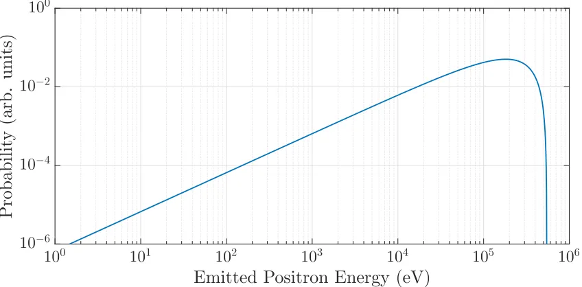
Figure 2.4: Distribution of emitted positron energy from22Na , calculated using the Fermi
equation for beta emission
positrons emitted from the source. A method is required to reduce the positron energy to
a range suitable for controlled beam formation and to perform the intended experimental
measurements. One way to reduce this energy is through the use of positron moderators.
There are various moderators used in positron experiments, including solid neon, nickel,
and tungsten, which are discussed in more detail in later in section 2.2.1.
Since we live in a matter dominated universe, a source of positrons is a rarity, and one
suitable for experimental purposes is harder still to obtain. Radioactive decay is one source
of positrons, and many isotopes emit this as one of their decay channels. Some of these
isotopes are naturally occurring, but ones used in laboratories are artificially produced
so that they are active enough for the count rates required for experiments. Artificial
production often means creating isotopes through enrichment at large scale facilities such
as cyclotrons, which can mean per gram antimatter is one of the most expensive items on
Earth. Table2.1lists some of the more commonly used sources of positrons for experiments
around the world.
Isotope β+ branching ratio Energy (MeV) Half-life
22Na 0.91 0.54 2.6 yr
58Co 0.15 0.47 70.8 d
18F 0.97 0.63 109 min
44Ti (44Sc) 1.0(0.94) (1.474) 60 yr (4 hr)
Table 2.1: Various atomic isotopes which produce positrons when they decay.
Positron tomography in medicine is a relatively common diagnostic tool. Cobalt-58
is used in medicine to test intestinal absorption of vitamin B-12 and is a tool which can
diagnose pernicious anaemia. Fluorine-18 is used in positron emission tomography (PET)
to locate cancerous growth in the body. The 18F is used to “label” sugars, which will
gather in areas of high metabolic rate, namely cancers or tumours. The 511keV photons
from positrons emitted by the 18F decay are picked up by position sensitive detectors,
allowing cancer sites to be located within the body [20].
Sodium-22 is a commonly used positron source for atomic and molecular physics
exper-iments, as well as materials science. The emitted positron energy and half-life make this
reaction:
Mg24(d, α)Na22 (2.2)
22Na is expensive to purchase, but with a∼2.6 year half-life a high activity quantity
enough to form an experimental source of positrons can last an experiment several years.
Titanium-44 has relevance for astrophysics as a potential candidate to account for
the abundance of galactic positrons, as titanium-44 is formed in particular supernovae
events [21]. It is also used by some groups for experimental physics with antimatter in
replacement of 22Na due to lack of access to a production facility [22]. 44Ti itself does
not emit positrons, however its daughter nuclei44Sc does. 44Ti decays at 100% branching
ratio to44Sc through electron capture, which then decays emitting a positron.
In addition to radioactive sources, pair production is used in some facilities as a method
to generate positrons. When high energy electrons in a cyclotron, linear accelerator, or
products from a nuclear reactor emit bremsstrahlung, pair production of positrons and
electrons will occur. The positrons can be used as a source for experiments when properly
collected and confined, however they typically have very high energy (≃30MeV). Several stages of energy reduction and confinement (beam bunching and chopping) are required to
bring the positrons down to low enough energy for experimental use, but source brightness
will typically remain very high.
2.2.1 Reducing Positron Energy
Slow and pulsed beam positron experiments make use of the positron sources mentioned
in the section above, however the initial energies and energy spread of the positrons are
not always suitable for experiments. To reduce the positron energy, interaction with
materials are used and these materials are known as “positron moderators”. There are
two commonly used types of of positron moderator: thin metal films, or rare gas solid
(RGS) based.
Metal foil moderators are thin foils of metals, typically tungsten or nickel. The
ef-ficiency for these materials as moderators varies between 0.1% to 0.001% depending on
the chosen metal [23,24]. They are relatively easy to build and maintain, but can require
metal films of the same material in moderation efficiency [25].
RGS moderators are harder to build but can provide higher efficiency. Neon is often
used, but argon and krypton can also be used. Neon has a lower freezing point than argon,
but has the highest efficiency spread of currently known moderators. The ability to create
RGS moderators in an experiment requires a cryogenic stage to cool your positron emitter
and grow a layer of solid gas close to it. Efficiency is approximately 0.7% for neon RGS
moderators and lower for argon and krypton [26]. The emitted positron energy spread
from RGS moderators is relatively high at around 1.5eV compared to approximately 0.5eV
for tungsten.
The trade off between RGS and metal foil moderators are effectively between efficiency
and energy spread. RGS moderators are more efficient with a larger energy spread, and
metal foil moderators are less efficient but have a smaller energy spread.
2.3
Positron Interactions with Matter
In this section an overview of the interactions between positrons and solid matter is
pre-sented in the context of a beam based PAS experiment [27].
Positrons can interact with solid in all of the various ways that matter particles do,
however as detailed previously positrons can also annihilate or form bound state
positro-nium.
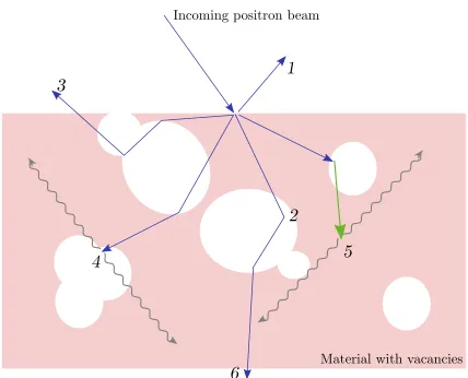
From the incoming positron beam, the majority of positrons will be implanted within
the material, but a small fraction can be reflected from the surface(1).
The implanted positron will interact with the material in ways which cause the positron
to lose energy, enabling other processes to occur. The positron loses energy through
interactions with the the constituent electrons and nuclei, for example ionisation, electronic
excitation, and nuclear scattering. These energy loss processes occur in the same manner
as ion implantation in general, and occur until the positron reaches the same temperature
as the material, ≃ 3/2kbT. The distance implanted positrons reach within a material is
important for PAS and explored in detail in section2.3.1.
The processes by which implanted positrons scatter is dominated by Coulomb
inter-actions. For this reason it is convenient to think of materials in terms of charge density.
4
5
1
6
2
3
Incoming positron beam
[image:31.595.117.545.94.440.2]Material with vacancies
Figure 2.5: Cartoon of the interactions of positrons from an incoming beam source. Num-bers reference processes detailed in the text.
become attractive or repulsive to the implanted positrons. Positron diffusion (2)is
influ-enced by the regions of effective charge and if defects are negatively charged (or neutral)
positrons will preferentially locate there. In a material with a large defect network, a
positron can move through the network and travel much larger distances than would be
possible without the presence of large electron-free volumes. In some cases, positrons that
enter a material like this can diffuse out of the material again, annihilating elsewhere
(3). Knowing the diffusion length of positrons in a material being studied can aid in the
interpretation of results for PAS experiments.
Thermalised positrons that diffuse through the material can annihilate (4), form
positronium (5), or escape the material through transmission(6).
In annihilation(4)the positron will annihilate with an electron from one of the atoms
that make up the solid. Generally this will be a valence electron - one furthest from
significant momentum. Annihilation with electrons in the bulk (rather than at a defect
site) will give the intrinsic lifetime of a material - how long the positron exists for within
the material before annihilating.
The formation of positronium(5)is possible in some materials, as long as the
positron-electron pair’s energy is above the 6.8eV binding energy. Following formation, the Ps can
further interact with the material before annihilation occurs.
2.3.1 Implantation of Positrons into Solid Materials
When positrons are implanted into a material, the depth z to which the positrons will
penetrate is dependent on the energy, E, of the incident positron and is modified by the
density, ρ, of the target. The formulation of the distribution of implanted positrons is
based on work by Makhov in 1961 on electron implantation [28,29].
The implantation profile is given by:
P(z, E) = mz
m−1
z0m exp − z z0 m (2.3)
z0 =
AEr ρΓ 1 + 1
m
(2.4)
The parametersA,m, and r are empirically determined, and the parameter values of
A = 4.0µgcm−2keV−r, m = 2, r = 1.6 are widely used based on the work of Vehanen et
al.[30].
The average distance an implanted positron travels through the material is given by
¯
z, the mean implantation depth. The calculation of ¯z uses the same constants as above:
¯
z= AE
r
ρ (2.5)
Theoretical work through Monte-Carlo simulation was performed by Valkealahti and
Nieminen to corroborate the work by Makhov resulted in the same profile and experimental
constants [31,32], however further simulation work was carried out by Ghosh showing that
the parameters for the profile vary with material [33].
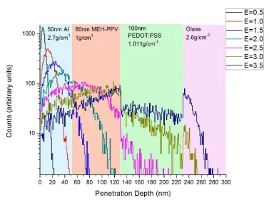
Figure 2.6: Makhov implantation profiles of various energy for aluminium (ρ= 2.70g/cm3).
The mean implantation depth ¯z is shown by the dashed line of the same colour for each energy plot.
for the same material sample, in this case aluminium. What is important to note is
that the distribution “smears out” as energy increases. The depth at which positrons
are implanted to doesn’t stay as tightly bunched at 2keV as for 1keV, and at 4keV the
positrons are sampling a range of depths in the aluminium sample over more than 400nm.
This can be a challenge for positron annihilation techniques as positrons implanted at
higher energies will also annihilate at the preceding depths in the sample. The mean
implantation depth is larger, but the relative percentage of positrons annihilating there
decreases, illustrated clearly with the values of ¯z shown on figure 2.6.
2.4
Positron Annihilation Lifetime Spectroscopy
Positron annihilation lifetime spectroscopy (PALS) is used to study the defect structure
(namely open volume defects) of materials, and the technique has been used and refined
for many years [34,35]. The lifetime of a positron is measured from a known starting time,
until a characteristic 511keV photon from positron-electron annihilation is detected,
re-peated over many measurements. Analysis of these lifetimes gives insight into the physical
properties exhibited by the material and in some cases the defect size can related to the
positron lifetime, for instance using the Tau-Eldrup model [36–41].
life-time within the material, ortho- and para- positronium characteristic lifelife-times if
positron-ium formation is possible within the the material, and a number of further lifetimes which
come from defects. The lifetimes from defects inside a material can range from specific
lifetimes, for example the di-vacancy in silicon has a positron lifetime of 320ps [42,43], or
a range of lifetimes for materials with a distribution of different sized defects. Comparison
of the presence of these lifetime characteristics in a material can reveal information on the
internal structure of the material sample.
Typically there are two types of PALS measurement, bulk PALS [44] and pulsed beam
PALS [45]. The two measurements differ in experimental set-up and the information gained
from the results, however theformof the results is the same. Bulk PALS systems are much
simpler than pulsed beam PALS and use as-emitted positrons from radioactive decay. The
positrons are therefore high energy with a large distribution of energies, meaning that they
will annihilate throughout the entire target and the bulk - hence the name, “bulk PALS”.
Pulsed beam PALS systems control the implantation energy of the positrons and therefore
probe only a selected region of the target, using a pulse of positrons which gives a specific
start point for the lifetime measurement.
2.4.1 PALS Data
A PALS spectrum is a histogram of positron lifetimes as observed from positrons implanted
into a particular material of interest. A typical histogram often contains 1−3.5×10⁶
counts. The spectrum typically shows a Gaussian resolution function convoluted with a
series of exponential decays for each present feature as mentioned previously.
The Gaussian resolution function is formed by the resolution in the detection system
in the experiment convoluted with the temporal width of the positron pulse.
To extract information from a PALS spectra, curve fitting programs are used to fit the
convolution of the resolution function and the positron lifetimes. The fitted exponential
decays give the lifetimes of positrons inside the material. The intensity is the amplitude
of the exponential decay. The generalised form of this is:
I0e−t
2/2σ2
Figure 2.7: An example PALS spectra, reproduced from the work by Saarinen and Ranki [46]. Here the PALS spectra of float-zone (Fz) refined silicon and Czochralski (Cz) grown silicon are compared after irradiation with 2MeV electrons. From the original work: “Positrons annihilate in the as-grown sample with a single lifetime of 220 ps corre-sponding to delocalized positrons in the lattice. In the irradiated samples the experiments reveal vacancies with positron lifetimes of 250 ps (V–As pair in Cz Si:As sample doped with [As] = 1020 cm−3) and 300 ps (divacancy in undoped FZ Si sample)”
where∗denotes the convolution. The coefficients are determined by fitting the spectrum, where I0e−t
2/2σ2
is the instrument function, and the Iie−τit terms are the lifetimes (τi)
and corresponding intensities (λi). An example of this data and fitting process is shown
in figure 2.7.
The intensity correlates to the relative presence of that lifetime, and in the case of
lifetimes arising from vacancies, correlates to the density of vacancies with that particular
positron lifetime. It can be thought of as the relative concentration of defects, although a
direct relationship between I and defect concentration is difficult to quantify.
2.4.2 Bulk PALS Systems
In a bulk PALS experiment, the material sample to be analysed is sandwiched between
22Na deposited on Kapton foil, and measurements are made using fast scintillation
detec-tors configured to collect the start and stop signals. The ‘start’ signal for the positron
the radioactive disintegration of a 22Na atom into 22Ne. The positron is emitted 3.7
pi-coseconds before the 1.27keV photon, see figure 2.3. These systems have good resolution
and can usually determine the intrinsic positron lifetimes of materials, even for metals,
which can be 100ps or less.
Since the positrons emitted in the decay of22Na have a large energy distribution and
are also of high energy, positrons that annihilate in the material will do so throughout
the whole sample without the possibility for singling out a particular depth or region of
interest within the sample. Additionally, since the22Na is deposited in some foil or other
layer outside of the sample, the material of the foil itself will interact in some way with
the emitted positrons, as radioactive decay is isotropic in emission direction. Positrons
may annihilate within the foil that they are prepared on, which can add complications to
analysing to the collected PALS spectra. The method also requires a lot of preparation
since a new radioactive source needs to be deposited on a foil for each sample measured.
2.4.3 Pulsed Beam PALS
Pulsed beam PALS forms positrons from a source into a controllable beam, and implants
the positrons into the target material in pulses at a well defined energy. The pulsing of
the beam gives the start signal for the lifetime measurement, and the annihilation photon
is again used as the stop signal. The pulsed beam system allows for depth profiling targets
with PALS since the energy of the positron pulse is defined by the experimental apparatus.
The simple model for the implantation depth of the positron beam is discussed in section
2.3.1.
The implantation distribution of the positrons is determined by the interaction energy
and so the energy of the positron pulse can be tailored such that annihilating positrons
sample regions of interest within the material being investigated. Preparation of samples
by irradiation can be systematically investigated from surface through to bulk.
Difficulties in these systems typically occur in the timing resolution of the experiment,
as this is determined by the temporal pulse width of the positrons. Trapping, bunching,
and accelerating positrons to form a pulsed beam is difficult task and many solutions have
2.4.4 Resolution of Lifetimes
The ability to resolve different lifetimes in a PALS spectrum depends on the full-width
at half-maximum (FWHM) of the resolution function in the experiment, as well as the
number of counts in the spectra. It is important to note that the FWHM does not limit
the experiment to only resolving lifetimes the same as or longer than the temporal width
of the FWHM. Collecting more data can allow you to resolve lifetimes shorter than the
inherent pulse width. However, in Poissonian statistics, the uncertainty scales as√n(the number of counts in the spectra), so diminishing returns will limit the practical benefit
to collecting more data for higher resolution. The impact of resolution and spectra total
counts was investigated by Yamawaki et al. [51].
2.4.5 The Tao-Eldrup Model
The relationship between positron lifetime and vacancy size was determined intially in a
semi-empirical model, the Tao-Eldrup model, and later reconciled in a more theoretical
framework relating to the quantum-mechanical size of the Ps wavefunction and in-material
cavity where it annihilates [38,39]. This work has more recently been reconsidered and
a fully quantum mechanical model was developed which agreed extremely well with the
previous Tao-Eldrup model [34,52]. Figure 2.8 illustrates the relationship between pore
dimension and positron lifetime for spherical or rectangular pores.
10-1 100 101 102 103
Pore dimension (nm)
0 20 40 60 80 100 120 140 160 P o si tr o n li fe ti m e (n s) Spherical model Rectangular model
It can be seen that the Tao-Eldrup model is not applicable to all systems with positron
lifetimes, and is un-physical for positron lifetimes below 400ps. For this reason it is
reliably used to relate positron lifetimes in molecular or organic materials, but not metallic
materials. The Tao-Eldrup model asymptotes to a lifetime of≃142ns, which is the lifetime of ortho-positronium in vacuum.
2.5
Doppler Broadening of Annihilation Radiation
Doppler broadening of annihilation radiation (DBAR) is a positron technique which
ob-tains information about the internal structure of a material by measuring the momentum
distribution of annihilation photons. DBAR is a comparative technique and the results
are unique to the particulars of the experimental apparatus used, however it is a
power-ful technique in determining the differences in internal structure of samples through the
changes in fractions of positrons that annihilate with electrons of different momentum.
DBAR can extract information on vacancies in materials and the chemical nature of
defects, and characterise changes in these properties as a function of depth through S and
W parameters respectively [53–55].
2.5.1 Doppler Broadening in Positron Spectroscopy
Generally speaking, when positron-electron annihilation takes place, the positron has
ther-malised within a material (Ee+ ≃ 3/2kbT, 40 milli-electron Volts at room temperature)
and hence has a low momentum. The other partner in the annihilation, the electron, does
not necessarily have a low momentum. Electrons in the outer shells or valence bands of
a material have low momentum, but the electrons which are much closer to the nucleus
can have very large momentum. In a case where a positron annihilates with a core shell
electron, the annihilation quanta undergo large Doppler shift due to the high momentum
of the core electron. Typically the Doppler broadening from positron annihilation with
valence shell electrons is ≃1keV, whereas positron annihilation with core shell electrons can result in broadening of ≥4keV.
In the frame of reference in which the centre of mass is at rest, the annihilation photons
the centre of mass is in motion from the momentum of the system, thus producing a
Doppler shift in the energy of the emitted gammas. The Doppler shift is give by:
∆E = 2mecvcmcosφ (2.7)
where φ is the angle between the motion of the centre of mass and one of the emitted
photons, andvcm is the speed of the centre of mass.
By analysing the annihilation photon energy from a particular target of interest, the
distribution of annihilation photon energies can be found. This allows a relative
measure-ment to be made, comparing the distributions of a damaged material with a pristine or
reference sample, which then gives information about the internal structure of the damaged
sample. Initial reporting of this phenomena was by DeBenetti in 1949 [56,57].
In an undamaged material, the distribution of photon energies is representative of the
physical structure of the material. In the case of a single crystal metal, the probability
of positron annihilation with valence or core electrons is the same throughout the whole
material sample. However, through damage a material may contain voids, dislocations, or
other defect types, and thus areas of effective negative charge are introduced. Positrons
implanted into a material like this will preferentially locate to these areas, and thus have a
higher probability of annihilating with a valence electron due to the lack of a neighbouring
atomic nuclei. This changes the annihilation photon energy distribution, and this can be
seen when comparing the damaged and pristine distributions [58,59].
In the comparison of positron annihilation distributions, two measurements are made:
the shape (S) parameter, and the wing (W) parameter measurements. These two
param-eters are comparisons of the area under a select region of the curve, in ratio to the total
area under the curve. The S and W parameter measurements each give information on
different aspects of the material being investigated.
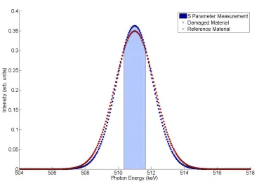
2.5.2 The S Parameter Measurement
The S parameter measurement is the ratio of the central peak in the spectra to the whole
area under the curve, as shown in figure2.9. The measurement region of the S parameter
is taken from the centre of the 511 peak to up to a few keV outwards. In figure 2.9, the
Figure 2.9: S parameter measurement region
An increase in S parameter signals an increase in the number of positrons annihilating
with low momentum electrons, and therefore an increase in the quantity of voids present in
the material. In a damaged sample there will be more 511keV photons from annihilation
from valence electrons in defect sites have the highest probability for annihilation.
S =
R
511+s511−s ndE
R
511+b511−b ndE
= Ns
Nb
(2.8)
For the work presented in this thesis in chapter 7 and 8, s is 1.2keV and defines the
central peak region, and bis 10keV, and defines the “whole area” of the peak.
The calculation of the uncertainty in the S parameter is based on Gaussian counting
statistics and given by:
σS =
1
√
Nb p
S(S+ 1) (2.9)
Depth profiling a sample with positrons and plotting the S parameter as a function
of depths is often a good way to find interesting features in a damaged sample, as the S
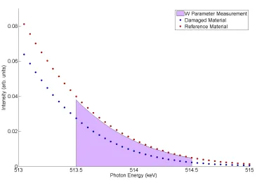
2.5.3 The W Parameter Measurement
Figure 2.10: W parameter measurement region
The W parameter measurement is the ratio of the high energy component of the spectra
to the whole area under the curve, as shown in figure2.10.
The W parameter measurement is generally taken in the region of 514 keV, so that
it does not interfere with the S Parameter measurement. The ratio is made using the
same limits for the whole peak area as the S parameter, which in the case of the work
presented in this thesis is 511±10keV. The W parameter gives information about the broadening due to high momentum electrons present in the material, which is determined
by the elemental species present.
Measurement of the high momentum region is harder to make than the S parameter
since the counts are fewer in this region than the centre of the 511keV photopeak and can
be swamped by background. This is particularly noticeable on the lower energy side of the
spectra, which has a higher background due to experimental effects (incomplete charge
col-lection, natural laboratory background radiation levels) and 3-photon annihilation events
from positrons.
back-ground on the low energy side of the 511keV photopeak, but can be almost entirely
re-moved through two detector coincidence measurements of two-photons annihilation events.
Without the 3-photon annihilation background both sides of the photopeak can be used
to make W parameter measurements [60].
Recently, mathematical processing of single detector DBAR measurements have been
developed to allow similar quality to coincidence experimental results [61].
To define the double sided W parameter measurement mathematically:
W =
R
514+wl514+wr
ndE+
R
508−wr
508−wl
ndE !
R
511+b511−b ndE
= Nw
Nb
(2.10)
The two integrals that make up the numerator of this ratio are the low energy (left) and
high energy (right) regions of the 511keV photopeak. The work presented in this thesis
makes use of a single detector system, so the W parameter measurements are defined using
the high energy side of the 511keV photopeak only, and the integrated region was from
514±1keV.
Since the W parameter is calculated in the same way as the S parameter, with similar
form but with different limits for integration, the expression for the uncertainty is the
similar:
σW =
1
√
Nb p
W(W + 1) (2.11)
This applies equally for single sided or double sided W parameter, as the uncertainty
in the numerator of equation2.10is still remains the square root of the sum of the counts.
2.5.4 Information From DBAR Measurements
Since DBAR makes relative measurements, it lends itself best to series measurements
across a sample set, which vary in preparation in a methodical manner. Each measured
sample will have S and W parameter measurements made in comparison to the same
pristine reference material.
Plotting the S and W parameter as a function of depth, preparation temperature, ion
evolution of the sample under these conditions.
Looking for significant changes in the S and W parameter trends indicates regions at
which the internal structure of a material is significantly changing. To fully characterise
the material, additional experimental measurements using absolute analysis techniques
(as opposed to relative analysis techniques, such as S and W parameter measurements)
[image:43.595.122.545.261.470.2]should be carried out at these critical regions.
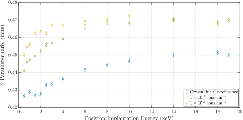
Figure 2.11: S parameter as a function of positron implantation energy for as-grown crys-talline germanium implanted with 1.5MeV germanium at 1×10¹¹and 1×10¹³ions·cm−2.
These measurements were made using the DBAR experiment developed as part of this work.
Figure 2.11 shows an example damage experiment which examines the effects of
im-planting as-grown crystalline germanium with germanium ions. The S parameter is
pre-sented as a function of positron implantation energy, which directly relates to mean
positron implantation depth. In this example, the S parameter is significantly larger
for the damaged samples of germanium substrate in comparison to the reference sample.
Additionally, the S parameter is larger for the sample implanted with a higher fluence
of germanium (1×10¹³ ions·cm−2) as compared to the sample implanted with the lower
fluence (1×10¹¹ ions·cm−2). The graph shows that the implantation has changed the
base material in a significant way, and the number of positrons annihilating with valence
2.6
Other Positron Techniques
There are other techniques to extract information from positron annihilation, in addition
to PALS and DBAR. Some examples are briefly described in the following sections.
2.6.1 Reflection High-Energy Positron Diffraction
Reflection high-energy positron diffraction (RHEPD) or total reflection high-energy positron
diffraction (TRHEPD) examines crystalline material surfaces, using glancing angles of
re-flection, or total reflection. Analysis of the diffraction patters gives information on the
surface formation, crystallographic orientation, and layering. The technique gives more
accurate results than similar techniques using electrons due to the differences between
positrons and electrons interacting with the crystal structure and diffraction laws as well
as very low levels of experimental background counts. RHEPD requires high intensity
positron beams to be effective and so is performed at bright positron sources, for example
KEK in Japan [62].
2.6.2 Angular Correlation of Annihilation Radiation
ACAR examines the deviation from co-linearity in the two-photon product in
positron-electron annihilation [56,57]. This examines the momentum of the annihilating pair
through position rather than direct measurement of photon energy. For this technique
to work properly it must be a coincidence measurement as the angle between the
anni-hilation photons must be determined relative to one another, requiring both photons to
be properly detected. The experimental set-up for an ACAR measurement tends to be a
large apparatus as increasing the distance between the detector and the sample increases
the angular resolution of the measurement. Ensuring the incident positron beam has a
small spot size at the target sample reduces the experimental uncertainty by reducing size
of the positron-electron annihilation region [63].
2.6.3 Age-Momentum Correlation
Age-MOmentum Correlation (AMOC) measurements combine PALS and DBAR
tech-niques which can reveal additional information by examining where the positron
start signal, a fast stop signal to obtain an accurate lifetime measurement, and an energy
measurement of the annihilation products for the annihilation photon momentum. An
AMOC measurement reveals patterns of movement of implanted positrons and positron
transport in the material (e.g. positrons could travel towards the bulk or become trapped
![Figure 2.7:An example PALS spectra, reproduced from the work by Saarinen andRanki [46].Here the PALS spectra of float-zone (Fz) refined silicon and Czochralski(Cz) grown silicon are compared after irradiation with 2MeV electrons](https://thumb-us.123doks.com/thumbv2/123dok_us/8207140.262360/35.595.212.444.105.352/reproduced-saarinen-andranki-rened-czochralski-compared-irradiation-electrons.webp)