International Journal of Innovative Technology and Exploring Engineering (IJITEE) ISSN: 2278-3075, Volume-8 Issue-9S3, July 2019
Abstract: This discourse used 45nm CMOS technology to design a Low noise amplifier for a Noise figure < 2dB and gain greater than 13dB at the 60GHz unlicensed band of frequency. A single stage, primary cascode LNA is modeled and its small signal model is analyzed. Common source structure is hired in the driver stage to escalate the output power with single stage contours. To enhance small signal gain, simple active transistor feedback and cascode feedback configurations are designed and appended to the basic LNA. In addition to this, current re-use inductor is designed and added to the cascode amplifier which is deliberated to give low power and low noise figure. Small signal analysis of simple active transistor feedback and current re-use inductor has been presented. The measurement results indicated that the input match and the output gain at 60GHz achieves -8dB and 13dB respectively with the supply voltage of 900mV. The frequency response obtained is a narrow band response with 6GHz of bandwidth. The circuit is simulated by Cadence Virtuoso tool. The layout of the related circuit is drawn by means of the Virtuoso Layout editor with total size of 0.1699μm2.
Index Terms: 60GHz, Current mirror feedback, LNA, low noise figure, RF amplifier.
I. INTRODUCTION
The contemporary evolution in CMOS technology at unlicensed 60GHz band. Suitable enough to meet the requirement at large scale wireless transceiver. The solitary promising application for 60-GHz for an increasing demand of multi-gigabit wireless networking. The efforts still have widely concentrated to operate on the 60-GHz band for point-to-point communication in consign with its low noise figure and gain. A low noise amplifier is one of the major blocks in the transceiver system. It is generally the first block of the receiver subsequent after the antenna. The LNA amplifies the input signals so that the noise generated in this block has a minor impact on the system signal to noise ratio (SNR) ratio. LNA circuits in CMOS technology are designed as Common Source (CS) or Common Gate (CG) stages. Another, cascode stage that is widely used in CMOS RF LNAs, can be considered as current –reuse configuration of a CS stage, followed by a CG stage. Common Source and Common Gate are two widely used transistor configurations in CMOS LNA circuits. CS LNA has high gain and good noise performance. Additional inductor in the source of a CS stage which is known to be Inductive Source degenerated. This additional inductor affects the gain and noise performance of LNA as discussed earlier. CG configuration
Revised Manuscript Received on July 22, 2019.
S. B. Rashmi, Don Bosco Institute of Technology, Bangalore, Karnataka, India.
Dr. S. Siva Yellampalli, Principal, UTL Technologies Ltd, VTU Extension Center, Bengaluru 560022.
has weak noise performance. Some techniques, such as capacitive cross coupling, have been presented to improve the CG stage noise performance. In this paper, the provocation and the research problem of 60-GHz networking are surveyed and illustrated. An amplifier elevates the power of both the signal and the noise present at its input. LNAs are sketched to attenuate additional noise.
The design in this paper has achieved a minimal noise figure by considering trade-offs that include impedance matching, selecting low-noise biasing conditions and output impedance matching circuit.
II. TRANSISTORMODEL
In RFIC’s design transistors are normally biased at a constant drain current density. The transistor’s power consumption normally a resultant of current and drain-source voltage VDS.
Further VGS is applied to achieve desired current density and it has no effect on dissipated dc power.
A. MOSFET high frequency performance
To characterize transistors RF performance at a chosen bias point following figure of merit are employed.
i. Cutoff frequency fT
ii. Maximum oscillation frequency fmax
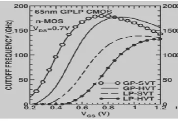
An evaluation of fT and fmax performance for selected
MOSFET from gpdk45 library. Figure 1 depicts the fT is
plotted against different gate-source voltage Vgs. Figure 2 shows the current density is plotted against cutoff frequency fT. This plot ensures the maxima of fT are achieved for a
current density of mA/um. This proves the selected MOS can yield a low power consumption and high frequency gain.
Figure1: fT versus gate source voltage
Design and Implementation of Low Noise
Amplifier At 60ghz using Current Mirror
Feedback
[image:1.595.334.516.581.704.2]Figure 2: current density versus cut-off frequency
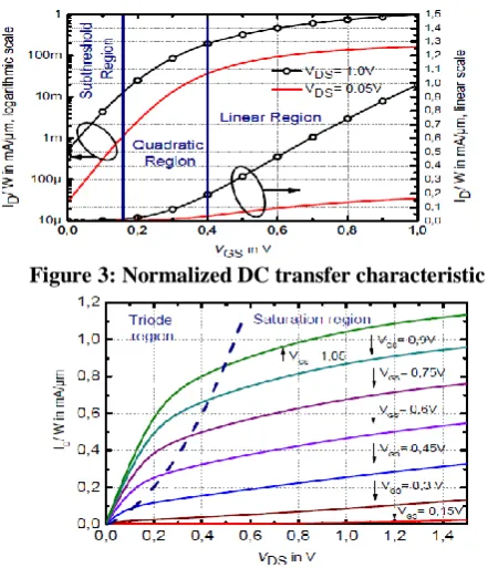
[image:2.595.69.255.55.160.2]Figure 3: Normalized DC transfer characteristic
Figure 4: output characteristics of 45nm nmos1v
Figure 3 shows the simulated DC transfer characteristics of a nmos1v n-channel MOSFET with L=45nm gate length. The graph depicts the pinch-off voltage of MOSFET is around 250-280mV. Figure 4. output characteristics of 45nm nmos1v n-channel MOSFET based on the simulation using gpdk models. Here to bias the low noise amplifier it need to be biased at Vgs=0.4V and Vds=1.2 V which yields a current density of 500uA/um.
III. PERFORMANCEMETRICSOFLOW-NOISE
AMPLIFIER
The performance metrics to be considered in designing an amplifier are small signal gain, input matching network, and output matching network, stability and band width. The general two port network of an amplifier is depicted in Figure 5.
Figure 5: Two-Port network of an amplifier
A. Power Gain:
Power Gain is defined as
in L
P
P
G
(1)
Transducer gain GT is defined as
a L T
P
P
G
(2) Available gain GA is defined as
a AT A
P
P
G
(3)
B. Linearity
The linearity issue existed depending on type of modulation scheme incorporated in modulation. In transmitter section if the amplitude modulation is incorporated then the power amplifier need to be linear region. In power amplifier the trade-off exist between efficiency and linearity. Assume that the input given to designed power amplifier is amplitude modulated wave (Vin(t)), if the power amplifier is highly
non-linear in nature. Then output of the amplifier Vd is given
by
)
(
)
(
)
(
)
(
t
a
1V
t
a
2V
2t
a
3V
3t
AV
V
d
in
in
in
in(4) This non-linearity need to be minimized in amplitude modulated output for recovering the information present in the envelop of the output.
C. Matching and Linearity
To get minimum noise figure using transistor the power reflection coefficient should match with ┌out* and load
reflection coefficient should match with ┌out
(5)
The overall performance of power amplifier is determined
by calculating GT. The proposed power amplifier MOSFET works at a power supply voltage of 1.8V. It is designed to deliver a output power of 10mW. It ensures the P1dB of 11.7dB and ┌opt of 0.815+j0.2209. The stability of the design
is ensured with the equation given 6 and 7.
21 12
2 2
22 2
11
2
1
S
S
S
S
K
=1.57>1 (6)21 12 22
11
S
S
S
S
=0.19<1 (7)D. Noise Figure
The one more component which need to be considered in designing low noise amplifier is its noise figure. Generally it is difficult to design an
[image:2.595.52.273.188.445.2]International Journal of Innovative Technology and Exploring Engineering (IJITEE) ISSN: 2278-3075, Volume-8 Issue-9S3, July 2019
trade-off is done between gain and noise figure to design consider constant gain circle and circle of constant noise figure. The noise figure is defined as
2
min S opt
S N
Y
Y
G
R
F
F
(8) Where
Ys= source admittance
Yopt=source admittance results in minimum noise figure Fmin=minimum noise figure when Ys=Yopt
RN= Equivalent noise resistance
Gs= real part of source admittance
IV. DESIGNOFLNAAT60GHZ
The important objective of LNA is to boost the low signals without appending the noise and for large signals it should intensify without establishing any distortion. As operating frequency is elevated, the threat in depicting LNA to endure its essentials increases. Some are (i) distributed parasitic affects the terminal impedance disturbing the resonant frequency of interest (ii) Scaling introduces short channel effects which degrade the performance of the circuit. Limit in the FOMs (Figure of Merit) of the device such as fT and fmax.
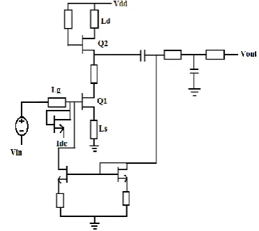
The basic LNA structure is shown in the figure 6. Which comprises of source degenerated cascode amplifier. Proper DC bias has been given. This circuit is based on attaining concurrent input matching with power contrived specification for attaining optimal noise figure. The transistor Q2 is in common gate configuration and configures cascode
with Q1. Size of Q2 transistor is approximately equal to that of
Q1. The transistor Q2 is included in the circuit to minimize the
direct coupling between the input and output. The load inductance increases the gain, as the current in an inductor will not change instantaneously. At the input side proper selection of Lg and Ls cancels the reactance offered.
Figure6: Basic source degenerated LNA Current mirror circuit
[image:3.595.91.249.477.609.2]Directed towards the evaluation of the proposed circuit, we have chosen a basic current mirror circuit as shown in the Figure 7. It consists of two branches that are parallel to each other and create two approximate equal currents. Let us consider the transistor M1 and M2 to be in saturation region
Figure7: Basic current source
For foremost enforcements, transistors should be matched and collector-base/drain-gate voltages should also be matched. This choice of circuit that has been taken as the output feedback plays a major role in elevating the gain of the LNA. The small signal model of current mirror and small signal model for low noise amplifier is shown in figure 8 and figure 9 respectively.
Figure8: Small signal model of current mirror
Figure9 Small signal model low noise amplifier
||
|| Z
A. Diode connected load
One more crucial criterion for LNA is to have a low noise figure. This can be achieved by a perfect input impedance matching.
Figure10: basic diode connected load
Figure11: Source degenerated low noise amplifier
This can be achieved by a resistor placed at the gate. Rather than using a resistor which is
[image:3.595.343.509.527.709.2]resistor by connecting gate and drain. This MOSFET can be used as diode connected load. The circuit diagram of basic diode connected load is depicted in figure 10.
B. Source degeneration
[image:4.595.336.522.52.217.2]Source degeneration can help obtaining a minimum noise figure and good input return loss simultaneously. In source degeneration either source may be connected to resistor or inductor. As resistor occupies more space in the layout inductor is used. Usage of inductor acts as a negative feedback to the circuit which increases the noise figure by decreasing the gain. The small signal equivalent model of source degeneration for proposed circuit. In reality the input of device is reactive, with real capacitive impedance due to Cgs. In order to remove the capacitive reactance and therefore
restore the FET input to a pure resistance, one way of achieving this is to add inductive feedback to the source. Additionally another inductor is added in series with the gate Lg that is selected to resonate with the Cgs capacitor. The
circuit diagram of source degenerated block of low noise amplifier is depicted in figure 11. Lg is designed so that at the resonate frequency it cancels out Cgs. The overall
performance of low noise amplifier is determined by calculating GT. The proposed LNA MOSFET works at a power supply voltage of 1.8V. It is designed to have noise figure of 1.002dB. It ensures the P1dB of 11.7dB and ┌opt of
0.815+j0.2209. The stability of the design is ensured with the equation given 10 and 11.
21 12
2 2
22 2
11
2
1
S
S
S
S
K
=1.57>1 (10)21 12 22
11
S
S
S
S
=0.19<1 (11) The equation for K and
ensures the unconditional stability of the circuit. From the figure it arbitrary assumed that the current density considered for low noise amplifier is 450uA/um. To enhance the gain and maintain the P1dB and noise figure number of active amplifying stages are increased. [image:4.595.306.546.602.832.2]V. PROPOSEDMETHODOLOGY
Figure 12 shows the proposed LNA circuit comprising of all the components designed in the subsections from I to iii. This is an cascoded amplifier which constitutes the inductive load Ld and Lg2 to nullify the capacitive reactance effects that is Cgs and Cdb on the circuit. The output matching is achieved
with the better matching circuit which improves the stability. The proposed LNA is shown in figure 7. Here cascode transistor Q2 is used to reduce the interaction of tuned output with tuned input. The Zout of the circuit is purely capacitive in nature, Ld load inductance used to resonates the total capacitance at the drain of Q2. This gives desirable higher gain at designed frequency. If narrow band response is required the input and output are commonly set. Transistor Q3 and Q4 forms a current mirror width of Q3 and Q4 are maintained to generate the desired current. The current through Q3 is set by output voltage. Gate biasing is provided by resistor designed by transistor Q5 implemented as diode connected load. The dc blocking capacitor C1 and C2 are used to prevent the variation of gate to source voltage of Q1 and output.
Figure12: proposed LNA with active current feedback
At designed frequency these blocking capacitors have negligible reactance. Some-times these capacitors are off-chip depending on the die area required. The circuit can be designed for operating frequency 60GHz, a 50Ω source resistance and a 50uA of bias current of Q1. Let’s assume the data for 45nm technology Leff is 38nm Cox=5fF/mm2. With this basic information width of main transistor Q1=7.5um at a bias current of 50uA. The unity gain frequency of this 45nm technology is about 120GHz, and the factor of α is found to be 0.85. Pessimistically assume that γ=2from the equation. From the equation 8 minimum noise figure is computed as 1.51dB, next the value of source degeneration inductance. To generate an input impedance of 50Ω Ls must be approximately 12nH considering the effect of Cgd. In order to compute Lg, Cgs of the selected device is approximately 200fF, to resonate this capacitor at resonating frequency 60GHz total inductance is about 35pH. Therefore Lg can be computed as 23pH. The design can be completed with the design of dc blocking capacitor which will be selected as 1pF in this design. In current mirror circuit to generate similar current same width is maintained for both main transistor and bias transistor. Here simple reference current source is used, it is advantageous to use constant –gm bias source to stabilize gain and input impedance temperature and supply. The cascode transistor is selected to have the same width as main transistor to some extent it can reduce the effect of miller capacitor. The gate and drain overlap capacitor can reduce the impedance looking in to the gate and drain terminals of M1 which in turn degrades the noise performance and input match. Figure13, depicts the small signal equivalent model of overall circuit
Figure13: small signal model of proposed LNA
The input impedance of the overall circuit is given
Z
International Journal of Innovative Technology and Exploring Engineering (IJITEE) ISSN: 2278-3075, Volume-8 Issue-9S3, July 2019
VI. RESULTS&DISCUSSION
The simulation of power amplifier is done by using a standard 45 nm CMOS process using Cadence virtuoso.
A. S- Parameter Analysis
The abbreviation S refers to scattering. Throughout the high frequencies, it is favorable to construct a given network in terms of microwaves than with voltages or currents. In occurrence, if we have 2 ports, then S11, S12, S21 and S22 represents input voltage reflection, reverse voltage gain, forward voltage gain and output voltage reflection respectively. S-parameters interpret the input-output analogy in the midst of ports in an electrical system. S11 expresses the power echoed from the antenna, Accordingly the input return loss(S11) simulated is -18dB at 63GHz as depicted in Figure 14.Through designing input matching circuit of maximum S11 can be accomplished. Extended with the above framework, the proposed PA attains an average gain S21 of10dB at 63GHz which is recognized as the frequency forward transmission coefficient is depicted in the Figure 15.
Figure14: S-Parameter S11 output
Figure15: S-parameter S21 output
B. Noise Figure
Noise figure (NF) is measures of degradation of the signal-to-noise ratio (SNR), caused by components in a radio-frequency (RF) signal chain. It is a number by which the performance of an amplifier or a radio receiver can be specified, with lower values indicating better performance. For a low noise amplifier the noise figure should be as low as possible. Obtaining an optimum noise figure at 60GHz is laborious job. The proposed circuit has obtained a noise figure less than 2 at the operating frequency. The Figure 16 shows the noise figure at operating frequency.
C. Layout of proposed LNA
Part of the manufacturing process which allows for the repetitive assembly of highly standardized products. When a manufacturing operation utilized product layout, production work can be layout in a straight line with labor and equipment subdivided in a smooth line. The process of calculation the
positions of the objects in space give the layout. The layout may be an arrangement, plan or a design. The layout has been simulated in layout editor which has been depicted in Figure 17 for the proposed circuit. The die area of the proposed PA occupies 0.1075µm2.
Figure16: Noise Figure
Figure17: Layout of proposed LNA
VII. CONCLUSION
In this paper, a narrow band LNA with a current mirror feedback technique has been presented. This circuit has been designed and simulated in a CADENCE VIRTUOSO 45nm technology. This LNA has a gain up to 13dB with a noise figure of 2dB for 60GHz frequency range.
REFERENCES
1. Ahmed, M., Shoaib, N., & Mahmood, I. (2011). Design, Analysis and Optimization of Multistage LNA at KU Band. Journal of Space Technology, 1, 95-100.
2. Borremans, J., Raczkowski, K., & Wambacq, P. (2009). A Digitally Controlled Compact 57-to-66 GHz Front-End in 45 nm Digital CMOS. Paper presented at the Solid-State Circuits Conference - Digest of Technical Papers, San Francisco, CA.
3. Chunhua, W., & Qiuzhen, W. (2011). A 0.18 um CMOS Low Noise Amplifier Using a Current Reuse Technique for 3.1–10.6 GHz UWB Receivers. Journal of Semiconductors, 32.
4. Cohen, E., Ravid, S., & Ritter, D. (2008). An Ultra Low Power LNA with 15dB Gain and 4.4 dB NF in 90nm CMOS Process for 60 GHz Phase Array Radio. Paper presented at the Radio Frequency Integrated Circuits Symposium, Atlanta, GA.
5. Fan, X., Zhang, H., & Sinencio, E. S. (2008). A Noise Reduction and Linearity Improvement Technique for a Differential Cascode LNA. IEEE Journal of Solid-State Circuits, 43(3), 588–599. doi:10.1109/JSSC.2007.916584
6. Feng, C., Yu, X. P., Lim, W. M., & Yeo, K. S. (2013). Compact 2.1–39 GHz Self-Biased Low-Noise Amplifier in 65 nm CMOS Technology. IEEE Microwave and Wireless Components Letters, 23(12), 662–664. doi:10.1109/LMWC.2013.2284778
7. Hsieh, C. A., Lin, Y. H., Hsiao, Y. H., & Wang, H. (2013). A 60 GHz Low Noise Amplifier with BuiltinLinearizer. Paper presented at the Microwave Symposium Digest (IMS), Seattle, WA. doi:10.1109/MWSYM.2013.6697369
8. Hsu, M. T., Du, J. H., & Chiu, W. C. (2012). Design of Low Power
CMOS LNA with
Engineering and Technology, 3(03), 167–174. doi:10.4236/wet.2012.33024
9. Huang, B. J., Wang, C. H., Chen, C. C., Lei, M. F., Huang, P. C., Lin, K. Y., & Wang, H. (2009). Designand Analysis for 60GHz Low Noise Amplifier with RF ESD Protection. IEEE Transactions on Microwave Theory and Techniques, 57(2), 298–305. doi:10.1109/TMTT.2008.2011158
10. Inui, C., Lai, I. C. H., & Fujishima, M. (2007). 60GHz CMOS Current-Reuse Cascade Amplifier. Paper presented at the Asia-Pacific Microwave Conference, Bangkok.
11. Kim, N., Aparin, V., Barnett, K., & Persico, C. (2006). A Cellular-Band CDMA CMOS LNA Linearized Using Active Post-Distortion. IEEE Journal of Solid-State Circuits, 41(7), 1530–1534. doi:10.1109/ JSSC.2006.873909
12. Kim, T. S., & Kim, B. S. (2006). Post-Linearization of Cascode CMOS LNA using Folded PMOS IMD Sinker. IEEE Microwave and Wireless
Components Letters, 16(4), 182–184.
doi:10.1109/LMWC.2006.872131
13. Kim, Y. M., Han, H., & Kim, T. W. (2013). A 0.6-V +4 dBm IIP3 LC Folded Cascode CMOS LNA With gm Linearization. IEEE Transactions on Circuits and Wystems. II, Express Briefs, 60(3), 122–126. doi:10.1109/TCSII.2013.2240811
14. Kuo, H. C., & Chuang, H. R. (2013). A 60-GHz High-Gain, Low-Power, 3.7-dB Noise-Figure. Paper presented at the 8th European Microwave Integrated Circuits Conference, Nuremberg.
15. Kuo, J. J., Tsai, Z. M., Lin, K. Y., & Wang, H. (2011). Design and Analysis of Novel Linearization Technique of Cascode Cell in a 60-GHz CMOS Demodulator. IEEE Transactions on Microwave Theory and Techniques, 59(2), 456–465. doi:10.1109/TMTT.2010.2095424
16. Lee, J. Y., Park, H. K., Chang, H. J., & Yun, T. Y. (2012). Low-Power UWB LNA with Common-Gate and Current-Reuse Techniques. IET Microwaves. Antennas & Propagation, 6, 793–799.
AUTHORSPROFILE
Rashmi S B done her BE in Electronics and Communication Engineering in 2004. M.Tech in VLSI and Embedded systems from VTU in2012. Currently she is perusing her PhD in RF CMOS design. Her area of interests are low noise amplifier design, power amplifier design and phase locked loops