http://eprints.whiterose.ac.uk/150110/
Version: Published Version
Article:
Henthorn, S. orcid.org/0000-0003-1913-9283, Ford, K. orcid.org/0000-0002-1080-6193
and O'Farrell, T. orcid.org/0000-0002-7870-4097 (2019) Direct antenna modulation for
high-order phase shift keying. IEEE Transactions on Antennas and Propagation. ISSN
0018-926X
https://doi.org/10.1109/TAP.2019.2935136
[email protected] https://eprints.whiterose.ac.uk/ Reuse
This article is distributed under the terms of the Creative Commons Attribution (CC BY) licence. This licence allows you to distribute, remix, tweak, and build upon the work, even commercially, as long as you credit the authors for the original work. More information and the full terms of the licence here:
https://creativecommons.org/licenses/
Takedown
If you consider content in White Rose Research Online to be in breach of UK law, please notify us by
Direct Antenna Modulation for high-order Phase
Shift Keying
Stephen Henthorn, Kenneth Lee Ford,
Senior Member, IEEE
, and Timothy O’Farrell,
Senior Member, IEEE
Abstract—An antenna capable of directly phase modulating a radio frequency carrier is discussed, designed, and measured as both an antenna and a modulator. Access point densification for the Internet of Things will be expensive in part due to the cost and inefficiency of amplifying waveforms with large peak-to-average power ratios for downlink transmission. Directly modulating at the antenna means only a carrier wave has to be amplified, reducing the cost of densification. Here, reconfigurable frequency selective surfaces are suggested as phase modulators. The design process for producing a phase modulating antenna is detailed, and a prototype is fabricated that is capable of up to 8-PSK modulation with 5.3dB variation in constellation points and a peak gain of 2.3dB. When implemented in an end-to-end communications system, the antenna exhibits only 1.5dB drop in performance compared with instrument grade modulation in an AWGN channel.
Index Terms—Cellular Radio, Continuous Phase Modulation, Phase Shift Keying, Frequency Selective Surfaces, Reconfigurable Antennas
I. INTRODUCTION
C
ONNECTING millions of devices in smart,reconfig-urable networks has the possibility to change the way public service delivery, civic infrastructure and industry op-erate. Developing the technology and communications infras-tructure for this Internet of Things (IoT) is a major challenge [1]. The main approaches to support so many devices have been either narrowband, such as NB-IoT and Weightless [2], [3], or wideband, such as Ingenu and LoRaWAN [4], [5]. Wideband technologies have the advantage of being interference-resilient, allowing operation in licensed or un-licensed bands, and are flexible in terms of the number of devices and data rates they can support [6]. This is particularly of interest on the IoT downlink, where many devices must have a near-constant link to enable smart network reconfiguration and resource allocation [7].
However, the wideband downlink approach would require an expansion of network infrastructure, increasing the number of base stations to support the millions of new connected devices. This increases the installation and running costs of the network. A large proportion of this cost is the downlink transmitter, and in particular the power amplifier (PA) [8] [9]. This is because, in traditional radio transmitter architectures, modulation occurs at low power, and the whole signal is am-plified to a relatively high power (Fig. 1a) [10]. The wideband
This work was funded by an EPSRC iCASE award with industrial sponsors NEC and BT.
The authors are with the Department of Electronic and Electrical Engi-neering, University of Sheffield, Sheffield, UK (e-mail: sdhenthorn1, l.ford, [email protected])
(a)
(b)
Fig. 1. (a) Block diagram of a conventional homodyne quadrature transmitter, (b) Concept diagram of a DAM transmitter using a reconfigurable antenna
IoT downlink signal would have a significant peak-to-average power ratio, which the PA must amplify without distortion. In order to do this, expensive linear PAs are operated at back-off, resulting in a drop in efficiency and increasing operating costs [11].
Several different approaches have been taken to overcome these issues. Constant envelope modulation techniques have been utilised in order to avoid distortion even when using non-linear PAs, for example Gaussian Minimum Shift Keying (GMSK) which was used in the GSM/EDGE cellular standards [12] [13]. Another research topic is PA design, in particular work on Doherty amplifiers [14]. At least two amplifiers are biased independently to amplify the lower voltages and peaks of the input signal separately, allowing efficiency to be maintained in back-off. Other developments in PA design for communications include the Chireix amplifier, which separates the input signal into distinct constant envelope signals, ampli-fies them separately then combines them [15]. Efficiency is improved particularly at lower input amplitudes, though this is again at the cost of greater complexity. Combinations of these approaches have also been explored [16].
[image:2.612.331.539.176.349.2]antenna, allowing time domain modulation [17]. This concept was further developed by using PIN diodes, and showing how these could be used to allow a patch antenna to transmit signals more broadband than its own bandwidth [18], [19]. A similar approach for ultra-wideband on-off keying (OOK) with a patch antenna is described in [20].
DAM techniques have also been developed to produce di-rectional modulation. In [21], a single element driven by a RF carrier wave is surrounded by passive reflectors with integrated PIN diodes. Switching these diodes allows for production of arbitrary constellations in a given transmit direction, with receivers at other locations seeing a significantly distorted constellation. This work is further developed in [22], while further work using arrays of elements driven by one source but using phase shifters to produce constellations has also been explored [23], [24].
Metamaterials have also been suggested as possible modula-tors in a DAM transmitter. [25] suggests integrating a bandpass reconfigurable frequency selective surface (FSS) with PIN diodes, as in [26], to switch the FSS between transmission and reflection in order to produce amplitude shift keying (ASK) modulation. There is the suggestion that this could allow high rate modulation at millimetre wave and terahertz transmit frequencies. More recently, an electrically large reflective metasurface loaded with varactor diodes has been shown to produce order 8 phase shift keying (PSK) modulation when illuminated by a plane wave [27].
The authors have previously proposed using transmissive FSS with integrated varactor diodes allowing control of the transmitted phase [28]. A proof-of-concept prototype capable of producing quadrature phase shift keying (QPSK) modu-lation is shown in [29], which shows modumodu-lation using this prototype can achieve a drop of only 4dB in SNR performance when using spread spectrum techniques. However, it is only capable of low order modulation and has low gain.
Similar work using FSS to vary transmitted phase has also been explored to produce beamsteering antennas. Using bandpass FSS which change the transmitted phase in order to beamform have been explored, creating a planar lens either in front of an antenna, as in [30], or incorporated in a resonant cavity, as in [31]. Again, there are proposals to make these reconfigurable by varying capacitance [32], [33] or by switching PIN diodes [34], [35]. Each of these techniques requires individual control of each unit cell.
[image:3.612.326.542.52.220.2]This paper presents a full characterisation and system imple-mentation of an antenna capable of phase DAM. By increasing the number of FSS layers, improvement over previous proof-of-concept demonstrations of FSS DAM has been achieved with up to at least 8-PSK modulation. The effects of different contributions of loss are examined, as are the effects of varying key design parameters. The DAM communications system in this paper is also improved, using a balancing code rather than direct sequence spread spectrum (DSSS) for amelioration of systematic distortions. This, along with the FSS design developments described above, produces a large improvement in the data rate, efficiency and bit error rate (BER) over previous work. In the next section, the concept and some challenges of using FSS for PSK DAM is described in Section
Fig. 2. Concept of DAM using a reconfigurable bandpass FSS
II. In Section III, the modulating antenna is designed and simulated in CST Microwave Studio, from unit cell to a FSS integrated antenna. The fabrication process and antenna measurements are described in Section IV. Finally, in Section V the modulating antenna is incorporated into an end-to-end communications system, with BER measurements shown for BPSK, QPSK and 8-PSK modulation in AWGN.
II. DIRECT ANTENNA MODULATION USING FREQUENCY
SELECTIVE SURFACES
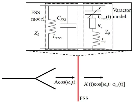
The concept of using FSS for directly modulating at the antenna is shown in Fig. 2. An FSS is placed in front of a passive antenna, transmitting a carrier wave at frequency ωc with amplitudeA. The FSS acts a bandpass filter, as shown by the equivalent circuit described in [36], with some inductance LF SS and capacitanceCF SS defining its resonant frequency. Variable capacitors are integrated with the FSS, adding in parallel a reconfigurable capacitance,Cvar, in series with some parasitic resistanceRsand inductanceLs. This reconfigurable capacitance allows tuning of the FSS centre frequency.
When the carrier wave is incident on the FSS and ωc is within the FSS passband, a phase change φm is produced, with some reduction in magnitude toA′
. Changing the centre frequency of the FSS allows control of φm with only small changes in A′
. This forms the basis of a phase modulator operating at the antenna.
III. DESIGN OF A PHASE MODULATING ANTENNA
In this section, the design process of a FSS-based modulat-ing antenna is discussed. For demonstration, the antenna will be capable of a single linear polarisation and operate at 1.8 GHz.
A. Frequency selective surface design for DAM
such, a broadband reconfigurable bandpass FSS design with stability over a reasonable range of angles of incidence should be chosen. A square loop slot design was chosen for these reasons, as well as its relatively small cell size for a given resonant frequency [36].
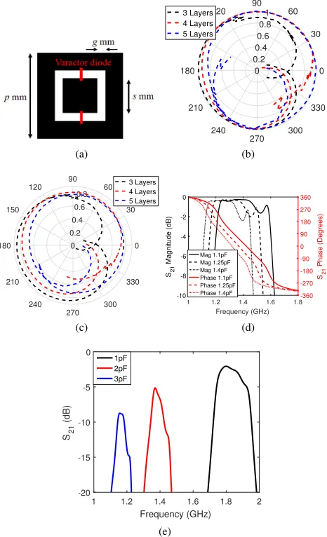
To achieve the arbitrary phase change required for PSK modulation, the devices reconfiguring the FSS should allow fine control of the resonant frequency. They should also have minimal loss, acceptable linearity and, for wideband modula-tion, be capable of switching rates in the MHz. Variable ca-pacitors allow continuous or near-continuous reconfigurability over a certain range, and types such as microelectromechanical systems (MEMS), barium strontium titanate (BST) tunable capacitors and liquid crystal capacitors have been demon-strated for use on FSS [37], [38], [39]. While MEMS and other digital capacitors have high linearity and low equivalent series resistances (ESRs), they have slow switching speeds and require complicated bias networks. BST capacitors are low loss, but due to their tuning mechanism the maximum switching rates with current commercial devices is in the kHz, while liquid crystal capacitors are in infancy. As such, due to their fast switching speeds, varactor diodes were chosen. In particular, the 1SV280 diode was chosen, due to its low ESR of0.44Ωand low capacitances. The model of the varactor used is shown in Fig. 2, with Rs=0.44Ω, Ls=0.6nH, and Cvar=1 - 4pF. For a single linear polarisation, diodes need only be integrated in line with the E-field of the incident wave, as shown in the final design of the unit cell (Fig. 3a).
Square-loop unit cells can be designed for a certain reso-nance using the equivalent circuit technique described by [36]. This describes the resonance of an FSS as some inductance LF SS and some capacitance CF SS in terms of the unit cell dimensions. Assuming a wave of normal incidence, the inductive impedance XL and capacitive susceptance BC can be calculated as follows
XL
Z0 =
(s+ 2g)
p F(p,2g, λ) (1)
BC
Z0 =
(4s+ 8g)
p F(p, p−s−2g, λ) (2)
wherep,sandg are the period, inner patch size and loop thickness respectively (Fig. 3a). FunctionF is defined as
F(p, w, λ) = p
λ[ln(cosec( wπ
2p)) +G(p, w, λ)] (3)
where
G(p, w, λ) =
1 2
(1−β2)2[(1
−β
2
4)(A++A−) + 4β
2A+A−]
(1−β42) +β
2(1 +β2
2 −
β2
8)(A++A−) + 2β
6A+A−
(4)
A±= q 1
1±λp22
−1 (5)
and (a) 0 30 60 90 120 150 180 210 240 270 300 330 0 0.2 0.4 0.6 0.8 1 3 Layers 4 Layers 5 Layers (b) 0 30 60 90 120 150 180 210 240 270 300 330 0 0.2 0.4 0.6 0.8 3 Layers 4 Layers 5 Layers (c)
1 1.2 1.4 1.6 1.8
Frequency (GHz) -10 -8 -6 -4 -2 0 S2 1 Magnitude (dB) -360 -270 -180 -90 0 90 180 270 360 S2 1 Phase (Degrees) Mag 1.1pF Mag 1.25pF Mag 1.4pF Phase 1.1pF Phase 1.25pF Phase 1.4pF (d)
[image:4.612.320.553.67.450.2]1 1.2 1.4 1.6 1.8 2 Frequency (GHz) -20 -15 -10 -5 0 S2 1 (dB) 1pF 2pF 3pF (e)
Fig. 3. (a) Schematic of reconfigurable FSS unit cell, (b) Free-space simulation of lossless FSS S21 with changing capacitance, (c) Free-space simulation of lossy FSS S21 with changing capacitance, (d) Free-space simulation of 4-layer lossy FSSS21with valuesp = 14mm,s= 12mm,
g= 0.6mm, (e) Free-space simulation of same FSSS21 over broad tuning range
β =sin(πw)
2p (6)
The calculated XL and BC can then be used to find the resonant frequency of the FSS for a given geometry. When varactor diodes are integrated onto the FSS, the equivalent circuit becomes as shown in the detail of Fig. 2.
In order to achieve 360o of phase change, a multi-layer FSS is required. To find the appropriate number of layers, the square loop design in Fig. 3a was simulated in CST with Floquet boundaries in free space while varying the diode capacitance, with theS21at 1.8GHz recorded. The simulation
used values p = 15mm, s = 12mm and g = 0.6mm,
Cvar=1pF to 4pF (Fig. 2). When a lossless substrate and lossless diodes were used, Fig. 3b is produced, showing that three layers has 5.3dB variation in transmitted magnitude over 360o phase change, four layers has 2.9dB variation, and five layers has 1.7dB variation. These values are larger than the theoretical limit discussed in [40], which gives 1dB variation for a four layer FSS. The discrepancy is due to the assumption for analysis in [40] that a single substrate material ofǫr=1 fills all the space between FSS layers, which does not hold when using any practical substrate with air gaps between layers. Further, any losses due to tuning are not considered in [40]. Despite this, the simulations performed suggest that that more layers provides better modulation performance.
However, adding a substrate loss tangent of tanδ = 0.025 and diode ESR of 0.44Ωto the model produces Fig. 3c. This shows that the magnitude variation with phase and the total loss through the FSS are affected by the increase in loss. For four layers, the variation is 3.1dB with a minimum loss of 1.8dB, while for five layers the variation is 1.7dB and the minimum loss is 2.3dB. As such, while increasing the number of layers reduces the amount of magnitude variation with phase change, it also increases the total loss through the FSS. This trade-off must be considered in the antenna design process. In this case, over the 315o required for an 8-PSK constellation, both 5 and 4 layer simulations show 1.4dB variation. As such, a four layer design was chosen, and the simulated S21 of this design in free space is shown against frequency in Fig. 3d. It should be noted that increasing the diode capacitance decreases the maximumS21of the FSS (Fig. 3e). This is because, at higher capacitances, the impedance of the diodes reduces at a given frequency, allowing more current to pass through. This then increases the I2R
losses in the diode resistance Rs. Further,Rs in varactor diodes is smaller at lower capacitances [41], though this has not been included in the simulation model here. As such, to minimise transmission loss, the FSS should be designed to operate at low capacitances.
B. Antenna design
In order to operate in a practical transmitter, the modulating FSS must be combined with an antenna. A free-space solution, with an element placed behind the multi-layered FSS, was found to be impractical due to the large physical size of FSS required to prevent the carrier diffracting around the FSS. As such, the FSS was integrated into a rectangular waveguide structure, ensuring all signals pass through all layers of the FSS. To inject RF into the waveguide, a monopole feed of lengthlis extended from an SMA connector and placed some distance from the FSS, here 57mm (Fig. 4a). A cavity backing is addedλ/4away from the monopole to ensure all the energy goes through the FSS, creating the final antenna design shown in Fig. 6a.
However, in a waveguide solution the FSS behaves differ-ently from the free space case, due to the change in wave impedance and the longer wavelength at 1.8GHz inside the waveguide. The FSS must be a finite-sized, with the strongest E-field at the centre of the x-plane [42]. Fig. 5a shows the
(a)
[image:5.612.327.544.59.356.2](b)
Fig. 4. Diagrams of modulating antenna concept. (a) 3D antenna structure, (b) FSS structure in antenna
0 30 60 90 120
150
180
210
240 270
300 330 0
0.2 0.4
0.6 0.8
1 3x34x4
5x5
(a)
1.7 1.8 1.9
Frequency (GHz)
-20 -15 -10 -5 0
Normalised farfield magnitude (dB)
42mm 47mm 52mm 57mm 62mm
(b)
Fig. 5. Simulated antenna against frequency forW = 112.5mm, (a) polar farfield magnitude for differentMxK numbers of unit cells at 1.5pF, (b) farfield magnitude with different spacings between FSS layersd= 35mm
[image:5.612.318.558.400.535.2](a)
[image:6.612.64.285.57.323.2](b) (c)
Fig. 6. Diagrams of antenna design. (a) Side view, (b) Front view, (c) Bias lines on reverse of FSS
The optimal spacing between layers of the FSS was also explored. Using the equivalent circuit analogy, to provide the flattest filter response a transmission line of a quarter of a wavelength is required between each LC combination. How-ever, within the cavity a quarter of a wavelength at transmit frequency is neither what it would be in free space,λ0/4, nor the theoretical wavelength in an infinitely long square waveg-uide of size W, λg = λ0/
q
1−(λ0
2W) 2
. Instead, it will be somewhere in between. In order to find this cavity wavelength λc, the full antenna structure was simulated with varying spacings at a fixed capacitance. Results for a waveguide of
W = 112.5mm and length L = 5
4λc is shown in 5b, with the flattest response being the optimum, here λc/4 = 57mm. Combinations of different spacings between FSS layers were also explored, but did not show any improvement in passband flatness.
The antenna also requires a biasing network to ensure all diodes are biased at the same time by the same voltage. However, this network should be designed to minimise the impact on the transmitted wave. As such, the design shown in Fig. 6c is used, with most of the bias lines with widthb=1mm running horizontally, orthogonal to the incident E-field. The vertical lines are placed only 5.5mm from the edge of the FSS, so that they are in a region where the E-field is relatively weak. Vias are used to connect the central patches of the FSS unit cells to the bias network. The bias lines add an upward shift of approximately 15MHz to the centre frequency of the FSS due to the added inductance, as well as an additional loss of 0.12dB.
The final antenna design is shown in Fig. 6. The antenna is designed to operate in the licensed mobile band at 1.8GHz,
1.25 1.3 1.35 1.4 1.45 1.5
Capacitance (pF)
-10 -8 -6 -4 -2 0
Normalised E-field magnitude (dB) -300 -200 -100 0 100 200 300
E-field phase (Degrees)
(a)
1.25 1.3 1.35 1.4 1.45 1.5
Capacitance (pF) -25
-20 -15 -10 -5 0
Simulated S
1
1
(dB)
(b)
Fig. 7. Simulated antenna with varying capacitance, (a) farfield magnitude and phase, (b)S11
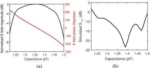
in line with expectations of using licensed mobile bands for IoT applications [43]. A 5×5 FSS was chosen with p = 22.5mm, s = 15mm, and g = 1mm, with the latter chosen to fit the diode footprint (Fig. 6b). This gives a cavity size
W = 0.675λ = 112.5mm and so optimum spacing λc/4 =
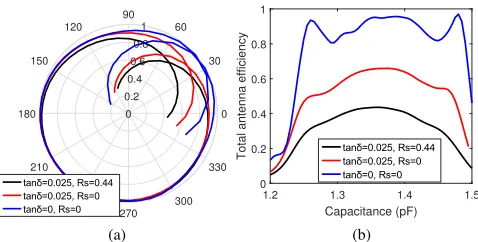
57mm and probe length l = 35mm. This is then simulated in CST with varying capacitance, with the diode assumptions given in Section III-B (Fig. 7a). The capacitance range of the passband is between 1.2pF and 1.5pF at the low tuning end of the 1SV280, minimising loss in the varactor diodes. The phase change in the pass band is greater than 360o, and the expected magnitude variation across this is 2.7dB. 1.3dB of the variation can be attributed to the diodes’ ESR, while 0.3dB is due to losses in the FSS substrate (see Fig. 8a).
[image:6.612.315.556.64.173.2]0 30 60 90 120
150
180
210
240 270
300 330 0
0.2 0.4 0.6 0.8
1
(a)
1.2 1.3 1.4 1.5
Capacitance (pF)
0 0.2 0.4 0.6 0.8 1
Total antenna efficiency
[image:7.612.365.510.54.240.2](b)
Fig. 8. Simulated antenna with varying capacitance for various loss config-urations (a) polar plot of antenna farfield, (b) total efficiency
1.6 1.7 1.8 1.9 2
Frequency (GHz) -20
-15 -10 -5 0
S1
1
(dB) 25mm
30mm 35mm 40mm 45mm
(a)
1.1 1.2 1.3 1.4 1.5 1.6
Capacitance (pF) 3
4 5 6 7 8
Simulated peak directivity (dB)
(b)
Fig. 9. (a) Simulated antennaS11against frequency with different lengths of monopole probelas a parameter, (b) Simulated directivity of antenna at 1.8GHz with changing capacitance
(a)
(b)
[image:7.612.53.292.64.185.2]Fig. 10. (a) Simulated amplitude of electric field in antenna cross-section, (b) Simulated surface currents on FSS 4 of antenna
Fig. 11. Photograph of fabricated DAM unit
IV. EXPERIMENTAL RESULTS
A. Antenna fabrication
The FSS was fabricated with standard PCB etching tech-niques, with copper conductor on 1.6mm thick FR4 board. 1SV280 varactor diodes were then soldered across the gaps of each FSS unit cell, all placed in line with the expected E-field. In order to fix the spacing of the FSS layers, holes were drilled in the corners of each FSS layer and a teflon threaded rod passed through, with teflon nuts holding each layer 57mm from the next. The antenna cavity was fabricated from sheet aluminium, with a hole drilled for a panel-mount SMA connector with its centre extended to 35mm. 2mm diameter holes were also drilled in the antenna side near where each FSS was to be placed to allow the biasing lines to be connected to wires, through RF chokes to a single coaxial cable for carrying the biasing signal. The cavity walls are held in place with conducting aluminium tape, and the final antenna is shown photographed in Fig. 11.
B. Antenna measurement
The salient characteristics of the antenna were then mea-sured, using a controllable voltage source to provide biasing.
The antenna S11 was measured using a Agilent E5071C
[image:7.612.53.289.232.339.2] [image:7.612.65.283.384.695.2]TABLE I
BIAS VOLTAGES FORBPSKCONSTELLATION USINGDAM
Data Constellation point Bias voltage (V)
0 -1 14.7
1 1 20.3
TABLE II
BIAS VOLTAGES FORQPSKCONSTELLATION USINGDAM
Data Constellation point Bias voltage (V)
00 1e−j3π/4 14.2
01 1ej3π/4
23.5
10 1ejπ/4
15.7
11 1e−jπ/4 18.6
TABLE III
BIAS VOLTAGES FOR8PSKCONSTELLATION USINGDAM
Data Constellation point Bias voltage (V)
000 1 22.1
001 1ejπ/4
25.3
010 1ej3π/4
14.5
011 1ejπ/2
13.9
100 1e−jπ/4 19.7
101 1e−jπ/2 17.7
110 1ejπ 15.2
111 1e−j3π/4 16.2
the peak, due to higher losses than expected, and also due to the higherS11than expected.
There is 10.6dB variation for 360o phase change, between 13.3V and 26.6V, but most of this occurs in the final 29o. As such, an 8-PSK constellation, which requires 315o phase change, can be created with 5.3dB variation between con-stellation points, shown by the dotted vertical lines in Fig. 12b. The variation in transmitted magnitude between these bias points manifests as a constellation with reduced amplitude at some angles, as shown in Fig. 13. The constellation point on the positive real axis is produced by the minimum bias voltage 13.9V, and increasing the bias voltage increases the transmitted phase from here (anticlockwise rotation). Fig. 13 also shows the variation in transmitted constellation observed over a range of viewing angles in both the E and H planes, showing a maximum of 15.6% variation in magnitude and 5.6o in phase for the H-plane over a 60o viewing angle. The E-plane beamwidth is smaller at 40o, and within this has a maximum of 12.1% variation in magnitude and 22o in phase. The bias voltages required for this are shown in Table III, and voltages that will provide constellations for BPSK and QPSK are shown in Tables I and II respectively.
The simulated and measured antenna radiation patterns are shown in Fig. 14 for the most and least transmissive constella-tion points measured. The peak gains differ between simulated and measured by 1.7dB at maximum transmission (black curves) and 4.1dB at minimum (red curves), showing a much steeper drop-off in magnitude at the edges of the response than expected. The measured beamwidth also decreases at extreme bias, from with a peak gain of 2.3dB and 3dB beamwidths of between 80oand 92oin the H-plane and 67oand 86oin the
E-14 16 18 20 22 24 26
Bias voltage (V)
-25 -20 -15 -10 -5 0 S1 1 (dB) Measured Simulated (a)
14 16 18 20 22 24 26 Bias voltage (V) -14 -12 -10 -8 -6 -4 -2 0
Normalised E-field magnitude
-100 0 100 200 300 400
Normalised E-field phase
Measured magnitude Simulated magnitude Measured phase Simulated phase
[image:8.612.94.260.259.354.2](b)
Fig. 12. Measured antenna with changing bias voltage, (a) reflection coeffi-cient at 1.8GHz, (b) Normalised farfield magnitude and phase
[image:8.612.312.575.390.502.2]0 30 60 90 120 150 180 210 240 270 300 330 0 0.2 0.4 0.6 0.8 1 -30 -15 0 15 30 (a) 0 30 60 90 120 150 180 210 240 270 300 330 0 0.2 0.4 0.6 0.8 1 -20 -10 0 10 20 (b)
Fig. 13. 8-PSK constellation produced by antenna at various viewing angles within beamwidth, (a) H-plane, (b) E-plane
-100 0 100
Angle (Degrees) -30 -20 -10 0 Gain (dBi) 15.7V 13.9V 1.38pF 1.46pF 15.7V (X-Pol) 13.9V (X-Pol) (a)
-180 -120 -60 0 60 120 180
Angle (Degrees) -40 -30 -20 -10 0 Gain (dBi) 15.7V 13.9V 1.38pF 1.46pF 15.7V (X-Pol) 13.9V (X-Pol) (b)
Fig. 14. Measured (voltage, dashed lines) and simulated (capacitance, solid lines) co-polar and cross-polar (dotted lines) pattern of antenna at 1.8GHz at peak and minimum transmission, (a) H-plane co-polar, (b) E-plane co-polar
plane. This is due to the known deficiency in diode modelling for FSS applications, as manufacturer models are based on diodes being applied in microstrip transmission lines, rather than being embedded in an FSS orthogonal to the direction of power flow. Similar effects can be seen in [44]. All the cross-polar components produced within these beamwidths are at least 14.2dB below the co-polar magnitude at that angle.
V. SYSTEM IMPLEMENTATION OF MODULATING ANTENNA
Fig. 15. System diagram for implementation of modulating antenna
A. Description of end-to-end communications system with modulating antenna
The system diagram of the communications system is shown in Fig. 15. Random binary data is generated on a PC in MATLAB, and then processed to produce a string of modulated symbols. These symbols are multiplied by a pulse-shaping sequencec(t), which here is either a rectangular pulse
represent by c(t) = rect(t) Tc
, whererect(t)is the rectangular function andTcis the chip period; or a Manchester code pulse,
where c(t) = [1,−1]· rect(t) Tc
. Using the Manchester code halves the throughput of the system, but means each PSK data symbol is composed of two PSK chips which will have different magnitudes when produced by DAM. This allows the magnitude variations to be averaged out at the receiver. Each data packet contained 1000 Bytes of data, which was preceded by a BPSK pilot sequence consisting of 50 iterations of the length 15 m-sequence.
The data chips are then sent to a Rohde & Schwarz SMBV100a signal generator, which maps the modulated data onto a non-linear voltage between -1V and 1V. This is then converted by some simple electronics into a bias voltage signal and connected by coaxial cable to the FSSs in the antenna. The 1.8GHz RF carrier wave is also provided by the signal generator, and is connected to the antenna’s RF feed. The antenna is placed facing into an anechoic chamber to ensure a simple AWGN channel, with a receiving horn antenna at boresight 1m away. The horn antenna is connected to a Rohde & Schwarz FSV Spectrum Analyzer, which samples the signal and sends this data to MATLAB in the PC. The received pilot sequence is correlated with the m-sequence to estimate a complex number defining the channel [6]. The conjugate of this channel estimate is multiplied with the received data chips to equalise the channel effects, and these equalised chips are then multiplied by the pulse shaping sequence c(t) and integrated over the symbol period Ts to recover the data symbols. A minimum distance detector was used to demodulate the symbols into binary data.
B. Measurement of system in AWGN
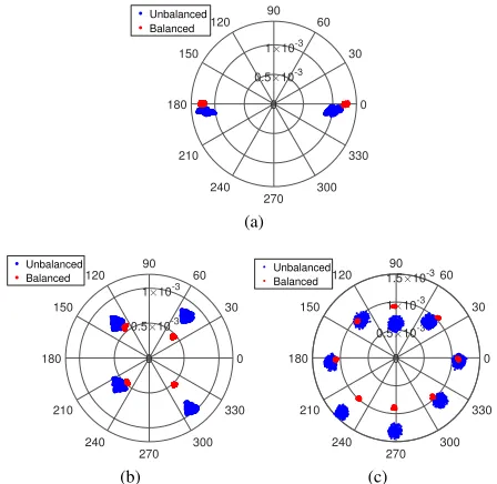
The setup measurement was performed in an anechoic chamber to minimise reflections and interference. The con-stellations produced are shown in Fig. 16, with c(t) as a rectangular pulse and as a Manchester code. The constellations shown are for BPSK, QPSK and 8-PSK, with transmission at
0 30 60 90 120
150
180
210
240
270 300 330 0
0.5 10-3 1 10-3 Unbalanced
Balanced
(a)
0 30 60 90 120
150
180
210
240
270 300 330 0
0.5 10-3 1 10-3 Unbalanced
Balanced
(b)
0 30 60 90 120
150
180
210
240
270 300 330 0
0.5 10-3 1 10-3 1.5 10-3 Unbalanced
Balanced
[image:9.612.48.290.59.152.2](c)
Fig. 16. Measured constellations produced by DAM in AWGN, Eb/N0=52dB, balanced and unbalanced. (a) BPSK, (b) QPSK, (c) 8PSK
1Msymbol/s and a constant Eb/N0 of 52dB. The amplitude variation between constellation points is 1.1dB for BPSK, 4.4dB for QPSK and 8.5dB for 8-PSK. When a Manchester code is used, these reduce to 0.03dB for BPSK, 1.8dB for QPSK and 2.0dB for 8-PSK, due to the averaging of the magnitude variation. It should also be noted that the EVM of the DAM constellation is noticeably larger than expected, with values of 7.4%, 8.3% and 8.2% for BPSK, QPSK and 8-PSK respectively. However, this reduces significantly when the Manchester code is used, to 2.3%, 4.0% and 2.4%. This suggests the variation is deterministic, and most likely caused by imperfections in the biasing signal sent to the direct antenna modulator. As such, improved driving of the antenna may improve the EVM further.
Bit error rate (BER) measurements are taken for each mod-ulation scheme, with and without using a Manchester code, and compared against instrument grade modulation from the SMBV1000a signal generator over the same channel (Fig. 17). For demonstration, the transmitter sample rate in each case is 1Msymbols/s. At each transmit power level, measurements were taken until 200 bit errors were observed and at least 10 packet errors were detected. The Eb/N0 was calculated by comparing the noise power to the average signal power across 100 different packets at the signal generator’s maximum transmit power to find a baseline. For BPSK, without balancing the DAM transmitter requires 2dB more transmit power to
achieve a BER of 10−5
compared with instrument grade modulation, whereas using a balancing sequence reduces this to nearly 0dB. For QPSK, the difference is approximately 1.5dB without balance, and 0.5dB with balance. Unbalanced 8PSK has an error rate which is only reducible to10−4
due to the distortion of the constellation, which in many practical communications systems would be considered poor. However, using a balancing sequence allows performance only 1.5dB worse at a BER of10−5
and reduction below10−6
0 5 10 15
Eb/No (dB)
10-6
10-4
10-2
100
BER
Theory DAM Unbalanced R&S Unbalanced DAM Balanced R&S Balanced
(a)
0 5 10
Eb/No (dB)
10-6
10-4
10-2
100
BER
DAM Unbalanced R&S Unbalanced DAM Balanced DAM Unbalanced Theory
(b)
0 5 10 15 20 25 Eb/No (dB) 10-6
10-4 10-2 100
BER
DAM Unbalanced R&S Unbalanced DAM Balanced R&S Balanced Simulation
[image:10.612.64.284.54.271.2](c)
Fig. 17. Measured bit error rates for DAM and instrument grade modulation in AWGN, balanced and unbalanced. (a) BPSK, (b) QPSK, (c) 8PSK
scenarios. Across all modulation orders, the instrument grade modulation follows the theoretical BER curve, showing the quality of this modulation, compared with the prototype DAM transmitter, which has some degradation, which increases with the modulation order.
This demonstrates significant advances over previous demonstrations of DAM using FSS [29]. By using four FSS layers rather than three, this work has increased the modulation order achievable from QPSK to 8-PSK. Compared with other DAM approaches, as shown in Table IV, this is equivalent to the modulation orders achieved by [27] and an advance over [20]. However, this comes at the cost of a greater physical depth than all the other approaches, reaching 1.71λ. This is still much smaller than the largest dimension of [27], which uses a metasurface of 5.44×1.36×0.07λ3
. It should also be noted that [27] requires a plane wave feed to the metasurface, which is not included in the dimensions given here. The solution in [20] is the most compact, at nearly a quarter of the aperture area of the DAM unit in this paper.
Compared with [29], the use of diodes with lower series resistance has improved the peak antenna efficiency from 10% to 46%. However, efficiency results are not given in [20], [27]. The symbol rate demonstrated in this paper is of a similar order to, but lower than, that achieved in [20], [27], though the same as [29]. Note, however, that these values are those demonstrated by practical testbeds, which are not necessarily the upper limits of each technique’s operation. Also, the carrier frequencies of each approach, which range from 1GHz to 4.25GHz, are those chosen for the design of these testbeds, and each approach is unlikely to be limited to only those given frequencies. Finally, while [29] uses a spreading code of length 15 to ameliorate the magnitude variation caused by FSS modulation, this work demonstrates good performance for BPSK and QPSK with no ameliorating technique, and amelioration of 8-PSK with a Manchester code, which has length 2. This increases the data throughput in
TABLE IV
COMPARISON OF KEY METRICS FORDAMTECHNIQUES
DAM technique
Modulation format
Operating Frequency (GHz)
Symbol rate (MSymbol/s)
Physical dimensions (λ3
)
This paper 8PSK 1.8 1 0.68×0.68×1.71
[29] QPSK 1.8 1 0.53×0.53×1.02
[27] 8PSK 4.25 2.048 5.44×1.36×0.07
[20] OOK 1 5 0.32×0.39×0.01
the same bandwidth. The sum effect of these advances is a smaller difference in BER performance between DAM and conventional modulation. Further, this paper is, to the authors’ knowledge, the only demonstration of DAM reaching BER performance of10−6
.
In all, this work has demonstrated a DAM solution with comparable symbol rates and operating frequencies to exist-ing solutions. It has a smaller form factor than [27], while producing higher order modulation than [29], [20].
VI. CONCLUSION
The first FSS-based direct antenna modulator capable of producing phase modulation up to 8-PSK has been presented, designed, characterised, and tested in an end-to-end com-munications system. The designed antenna was simulated to have a peak efficiency of 46% and magnitude variation of 2.7dB over 360oof phase change. Measurement found a peak gain of 2.3dB, and 6dB variation for 315o of phase change. The transmitted constellation was consistent in magnitude and phase within the antenna 3dB beamwidth of 60o in the H-plane and 40oin the E-plane. When a balancing code is used, the DAM transmitter produces constellations with EVM of the order of 2%. The BER performance of the DAM transmitter, when compared with instrument grade modulation, is impaired by 0dB, 2dB and 1.5dB for binary, quaternary and 8PSK respectively. Future work will examine the effects of lower loss materials, explore the possibility of amplitude modulation, and implement DAM in multipath communications systems.
REFERENCES
[1] M. R. Palattella, M. Dohler, A. Grieco, G. Rizzo, J. Torsner, T. Engel, and L. Ladid, “Internet of Things in the 5G era: Enablers, architecture, and business models,”IEEE Journal on Selected Areas in Communica-tions, vol. 34, no. 3, pp. 510–527, 2016.
[2] Y. E. Wang, X. Lin, A. Adhikary, A. Grovlen, Y. Sui, Y. Blankenship, J. Bergman, and H. S. Razaghi, “A primer on 3GPP narrowband Internet of Things,”IEEE Communications Magazine, vol. 55, no. 3, pp. 117– 123, 2017.
[3] A. Woolhouse, “The Weightless standard,” 2018. [Online]. Available: http://wireless.ictp.it/tvws/book/11.pdf
[4] T. J. Myers, “Random phase multiple access system with meshing,” 2010.
[5] A. Augustin, J. Yi, T. Clausen, and W. M. Townsley, “A study of LORA: Long range & low power networks for the Internet of Things,” Sensors (Basel, Switzerland), vol. 16, no. 9, p. 1466, 2016. [Online]. Available: http://www.ncbi.nlm.nih.gov/pmc/articles/PMC5038744/ [6] A. Goldsmith,Spread Spectrum Wireless Communications. Cambridge
University Press, 2005.
[image:10.612.316.559.83.133.2][8] A. Arbi and T. O’Farrell, “Energy efficiency in 5G access networks: Small cell densification and high order sectorisation,” in2015 IEEE International Conference on Communication Workshop (ICCW), Con-ference Proceedings, pp. 2806–2811.
[9] W. Guo and T. O’Farrell, “Capacity-energy-cost tradeoff in small cell networks,” in2012 IEEE 75th Vehicular Technology Conference (VTC Spring), Conference Proceedings, pp. 1–5.
[10] B. Arya, Radio Receiver and Transmitter Architectures. Wiley-IEEE Press, 2008, p. 224. [Online]. Available: http://ieeexplore.ieee.org/xpl/ articleDetails.jsp?arnumber=5224911
[11] S. C. Cripps,RF Power Amplifiers for Wireless Communications, Second Edition (Artech House Microwave Library (Hardcover)). Norwood, MA, USA: Artech House, Inc., 2006.
[12] 3GPP, “GSM/EDGE Modulation,” 3rd Generation Partnership Project (3GPP), Technical Specification (TS) 45.004, 06 2001, version 4.0.0. [Online]. Available: https://portal.3gpp.org/desktopmodules/ Specifications/SpecificationDetails.aspx?specificationId=2708
[13] K. Murota and K. Hirade, “GMSK modulation for digital mobile radio telephony,”IEEE Transactions on Communications, vol. 29, no. 7, pp. 1044–1050, 1981.
[14] W. H. Doherty, “A new high efficiency power amplifier for modulated waves,”Proceedings of the Institute of Radio Engineers, vol. 24, no. 9, pp. 1163–1182, 1936.
[15] T. W. Barton and D. J. Perreault, “Theory and implementation of RF-input outphasing power amplification,”IEEE Transactions on Microwave Theory and Techniques, vol. 63, no. 12, pp. 4273–4283, 2015. [16] H. Jang, R. Wilson, T. Canning, D. Seebacher, C. Schuberth, B. Arigong,
F. Trang, and S. Ward, “RF-input self-outphasing Doherty–Chireix combined amplifier,” IEEE Transactions on Microwave Theory and Techniques, vol. 64, no. 12, pp. 4518–4534, 2016.
[17] V. F. Fusco and C. Qiang, “Direct-signal modulation using a silicon mi-crostrip patch antenna,”Antennas and Propagation, IEEE Transactions on, vol. 47, no. 6, pp. 1025–1028, 1999.
[18] S. D. Keller, W. D. Palmer, and W. T. Joines, “Electromagnetic modeling and simulation of a directly modulated patch antenna,”Antennas and Wireless Propagation Letters, IEEE, vol. 9, pp. 779–782, 2010. [19] ——, “Switched antenna circuit with increased information bandwidth,”
IEEE Antennas and Wireless Propagation Letters, vol. 9, pp. 1045–1048, 2010.
[20] S. Srivastava and J. J. Adams, “Analysis of a direct antenna modulation transmitter for wideband OOK with a narrowband antenna,” IEEE Transactions on Antennas and Propagation, vol. 65, no. 10, pp. 4971– 4979, 2017.
[21] A. Babakhani, D. B. Rutledge, and A. Hajimiri, “Transmitter archi-tectures based on near-field direct antenna modulation,” Solid-State Circuits, IEEE Journal of, vol. 43, no. 12, pp. 2674–2692, 2008. [22] ——, “Near-field direct antenna modulation,” Microwave Magazine,
IEEE, vol. 10, no. 1, pp. 36–46, 2009.
[23] S. Hongzhe and A. Tennant, “Simultaneous, multichannel, spatially directive data transmission using direct antenna modulation,”Antennas and Propagation, IEEE Transactions on, vol. 62, no. 1, pp. 403–410, 2014.
[24] M. P. Daly and J. T. Bernhard, “Directional modulation technique for phased arrays,”Antennas and Propagation, IEEE Transactions on, vol. 57, no. 9, pp. 2633–2640, 2009.
[25] G. I. Kiani, T. S. Bird, and K. L. Ford, “60 GHz ASK modulator using switchable FSS,” inAntennas and Propagation Society International Symposium (APSURSI), 2010 IEEE, Conference Proceedings, pp. 1–4. [26] T. K. Chang, R. J. Langley, and E. Parker, “An active square loop
frequency selective surface,”IEEE Microwave and Guided Wave Letters, vol. 3, no. 10, pp. 387–388, 1993.
[27] W. Tang, “Programmable metasurface-based RF chain-free 8PSK wire-less transmitter,” Electronics Letters, vol. 55, pp. 417–420(3), April 2019.
[28] S. Henthorn, K. L. Ford, and T. O’Farrell, “Frequency selective surface loaded antenna for direct antenna modulation,” in2017 11th European Conference on Antennas and Propagation (EUCAP), March 2017, pp. 731–734.
[29] S. Henthorn, K. L. Ford, and T. O’Farrell, “Bit error rate performance of quadrature modulation transmission using reconfigurable frequency selective surfaces,”IEEE Antennas and Wireless Propagation Letters, vol. PP, no. 99, pp. 1–1, 2017.
[30] H. A. Ahmed, Y. Fan, Z. E. Atef, N. Payam, and A. B. Constantine, Analysis and Design of Transmitarray Antennas, ser. Analysis and Design of Transmitarray Antennas. Morgan & Claypool, 2017. [Online]. Available: http://ieeexplore.ieee.org/xpl/articleDetails. jsp?arnumber=7833475
[31] A. Epstein, J. P. S. Wong, and G. V. Eleftheriades, “Cavity-excited Huygens’ metasurface antennas for near-unity aperture illumination efficiency from arbitrarily large apertures,” Nature Communications, vol. 7, p. 10360, 2016. [Online]. Available: http://dx.doi.org/10.1038/ncomms10360
[32] J. R. Reis, N. Copner, A. Hammoudeh, Z. M. E. Al-Daher, R. F. S. Caldeirinha, T. R. Fernandes, and R. Gomes, “FSS-inspired transmitar-ray for two-dimensional antenna beamsteering,”IEEE Transactions on Antennas and Propagation, vol. 64, no. 6, pp. 2197–2206, 2016. [33] M. Sazegar, Y. Zheng, C. Kohler, H. Maune, M. Nikfalazar, J. R.
Binder, and R. Jakoby, “Beam steering transmitarray using tunable frequency selective surface with integrated ferroelectric varactors,”IEEE Transactions on Antennas and Propagation, vol. 60, no. 12, pp. 5690– 5699, 2012.
[34] A. Clemente, L. Dussopt, R. Sauleau, P. Potier, and P. Pouliguen, “1-bit reconfigurable unit cell based on PIN diodes for transmit-array appli-cations in X-band,”IEEE Transactions on Antennas and Propagation, vol. 60, no. 5, pp. 2260–2269, 2012.
[35] F. Diaby, A. Clemente, L. D. Palma, L. Dussopt, K. Pham, E. Fourn, and R. Sauleau, “Linearly-polarized electronically reconfigurable trans-mitarray antenna with 2-bit phase resolution in Ka-band,” in 2017 International Conference on Electromagnetics in Advanced Applications (ICEAA), Conference Proceedings, pp. 1295–1298.
[36] R. J. Langley and E. A. Parker, “Equivalent circuit model for arrays of square loops,”Electronics Letters, vol. 18, no. 7, pp. 294–296, 1982. [37] O. Bayraktar, O. A. Civi, and T. Akin, “Beam switching reflectarray
monolithically integrated with RF MEMS switches,”IEEE Transactions on Antennas and Propagation, vol. 60, no. 2, pp. 854–862, 2012. [38] M. Haghzadeh, L. M. Bhowmik, C. Armiento, and A. Akyurtlu, “Printed
tunable miniaturized frequency selective surface with BST/polymer composite filled interdigital capacitors,” in 2014 USNC-URSI Radio Science Meeting (Joint with AP-S Symposium), Conference Proceedings, pp. 154–154.
[39] W. Hu, R. Dickie, R. Cahill, H. Gamble, Y. Ismail, V. Fusco, D. Linton, N. Grant, and S. Rea, “Liquid crystal tunable mm wave frequency selective surface,”IEEE Microwave and Wireless Components Letters, vol. 17, no. 9, pp. 667–669, 2007.
[40] A. H. Abdelrahman, A. Z. Elsherbeni, and F. Yang, “Transmission phase limit of multilayer frequency-selective surfaces for transmitarray designs,” IEEE Transactions on Antennas and Propagation, vol. 62, no. 2, pp. 690–697, 2014.
[41] Toshiba, “1SV280 Variable Capacitance Diode,” 2014. [On-line]. Available: https://toshiba.semicon-storage.com/info/docget.jsp? did=2796\&prodName=1SV280
[42] N. Marcuvitz,Waveguide handbook. Institution of Electrical Engineers, 1986.
[43] NOKIA, “LTE evolution for IOT connectivity,” 2017. [Online]. Available: https://resources.ext.nokia.com/asset/200178
[44] J. Roberts, K. L. Ford, and J. M. Rigelsford, “Secure electromagnetic buildings using slow phase-switching frequency-selective surfaces,” IEEE Transactions on Antennas and Propagation, vol. 64, no. 1, pp. 251–261, 2016.
Stephen Henthorn received the M.Eng (First Class Hons.) degree in Electronic and Communica-tions Engineering from the University of Sheffield, Sheffield, U.K. in 2015, winning the Professor Sharom Ahmat Prize for performance in final year.
Kenneth Lee Ford (M’07 - SM’10) received the B.Eng. and Ph.D. degrees in electronic engineering from the University of Sheffield, Sheffield, U.K. in 1998 and 2003, respectively.
In 2001, he joined the Stealth Materials Depart-ment, Advanced Technology Centre, BAE Systems, Towcester, U.K. In 2005, he joined the University of Sheffield as a Lecturer of communications, and became a Senior Lecturer in 2012. His current research interests include reconfigurable antennas, miniaturized antennas, metamaterials, propagation in the built environment, and electromagnetic structures for biomedical applica-tions.
Timothy O’Farrell (M’91 - SM’18) received the M.Sc. (Distinction) and Ph.D. degrees from the University of Manchester, Manchester, U.K., in 1986 and 1989, respectively. In the framework of Mobile VCE (mVCE), he was the Academic Coordinator of the Core 5 Green Radio project from 2009 to 2012 and a Leader in establishing energy efficiency as a global research field in wireless communication systems. He is currently leading the FARAD Project and the U.K. Research Strategy Community Organ-isation in Communications, Mobile Computing, and Networking within the EPSRC portfolio. He is currently the Chair Professor of wireless communications with the University of Sheffield, Sheffield, U.K. He has managed 26 major research projects as a Principal Investigator. He has authored 315 journal and conference papers, book chapters, patents, and technical reports, and has participated in standards, consultancy, and expert witness activities within the wireless sector. He has pioneered research on energy efficient mobile cellular communications, the mathematical modelling of carrier sense multiple access-based MAC protocols for WiFi, coded modu-lation techniques for optical wireless communication systems, and spreading sequence design for CDMA wireless networks. His current research interests include wireless communication systems specializing in physical layer signal processing, radio resource management, and wireless network planning.