DESIGN AND SIMULATION OF MILLIMETER WAVE FILTER FOR NEXT GENERATION (5G) RF FRONT-END TRANSCEIVER
MUHAMMAD NADZMI BIN MOHD ZAIN
This report is submitted in partial fulfilment of requirement for the Bachelor Degree of Electronic Engineering (Telecommunication Engineering)
Fakulti Kejuruteraan Elektronik dan Kejuruteraan Komputer (FKEKK) Universiti Teknikal Malaysia Melaka (UTeM)
ii
UNIVERSTI TEKNIKAL MALAYSIA MELAKA
FAKUL Tl KEJURUTERAAN ELEKTRONIK DAN KEJURUTERAAN KOMPUTER
UN/VEa:Sllt IEKJira<Al WALAY31A fAEUtKA
BORANG PENGESAHAN STATUS LAPORAN
PROJEK SARJANA MUDA II
Tajuk Projek
: DESIGN AND SIMULATION OF MILLIMETER WAVE FILTER FOR NEXT GENERATION (SG) RF FRONT-END TRANSCEIVER
Sesi Pengajian 6 I 7
Saya MUHAMMAD NADZMI BIN MOHD ZAIN
(HURUF BESAR)
mengaku membenarkan Laporan Projek Sarjana Muda ini disimpan di Perpustakaan dengan syarat-syarat kegunaan seperti berikut:
1. Laporan adalah hakmilik Universiti Teknikal Malaysia Melaka.
2. Perpustakaan dibenarkan membuat salinan untuk tujuan pengajian sahaja.
3. Perpustakaari dibenarkan membuat salinan laporan ini sebagai bahan pertukaran antara institusi pengajian tinggi.
4. Sila tandakan ( '1 ) :
D
SULIT*D
TE RH AD**TIDAK TERHAD
:2./6/ !.f
Tarikh: ... ..
*(Mengandungi maklumat yang berdarjah keselamatan atau kepentingan Malaysia seperti yang termaktub di dalam AKTA RAHSIA RASMI 1972)
**(Mengandungi maklumat terhad yang telah ditentukan oleh organisasi/badan di mana penyelidikan dijalankan)
iii
"I hereby declare that this thesis entitled, Design and Simulation of Millimeter Wave
Filter for Next Generation (5G) RF Front-End Transceiver is a consequence of my own research idea concept for works that have been cited clearly in the references."
A~
SIGNATURE: ... .
NAME: MUHAMMAD NADZMI BIN MOHD ZAIN
2Y
/"
6/ {
iv
"I hereby declare that I have read this report and in my opinion, this report is sufficient in terms of scope and quality for the award of Bachelor of Electronic and
Computer Engineering (Telecommunication Engineering) with Honors."
SIGNATURE:
NAME: PM. DR. ZAHRILADHA BIN ZAKARIA
£f-v
It is my deepest gratitude and warmest affection that I dedicate this thesis to PM. DR. Zahriladha Bin Zakaria who has been a constant source of knowledge and
inspiration.
vi
ACKNOWLEDGEMENT
First and foremost, I would like to praise to Allah S.W.T for giving me an ability and strength to do my final year project succeed and complete my report as required. I would like to express my gratitude to my supportive and caring
supervisor, PM. DR. Zahriladha Bin Zakaria for providing his insightful knowledge and valuable assistance throughout this project under his guidance.
I would like to take a chance to thank all the lecturers who taught me in the past four years and great contribution that qualify me to do my final year project. I would like to thank DR. Ahmad Sadhiqin Bin Mohd Isira and PM. DR. Kok Swee Leong and the other lecturers and staff that participated to arrange for iNOTEK and IoT competition, with their efforts in providing information and cooperation to help students achieving the goals of final year projects.
At the other side of appreciation is extended to my parents, for their support and encouragement throughout my studies. Their advices and reminder always give me a strengthen to complete my final year project and studies. I would like to thank all senior students who helped me to clear out the questions and guide on the software that I use for this final year project.
vii
ABSTRACT
In RF Front-End is very important to provide a convenient interface between electromagnetic fields and (often digital) signal processing. For most
telecommunications systems, this interface is bidirectional since it consists of both a transmitter and receiver front end. However, RF front end the gain is to convert the weak signals and frequency to convenient amplitude levels for further processing. This project aims to design and simulate a filter that can the millimeter wave at 28GHz for next generation (5G) RF Front-End Transceiver. The method used is substrate integrated waveguide (SIW) which that capable of the design of devices of low radiation, low insertion loss and high Q. In addition, the whole components are constructed by metallic-post in dielectric structure. The via hole of the SIW will be in between of the dielectric and made the via hole as a wall replacing the solid wall of the rectangular waveguide. CST Studio Suite software is used to design the filter. Once the simulation has done, the optimization carried by using parametric studies by changing the width and length of the t-shape metal and the distance of the pitch. The filter operating at frequency 28GHz with the return loss less than -10dB and wide bandwidth greater than 1GHz. Comparison of the filter performance is carried, in terms of filter parameters such as return loss, insertion loss, efficiency and
viii
ABSTRAK
Dalam penghasilan RF Hadapan-Akhir adalah sangat penting untuk menyediakan antara muka yang mudah antara medan elektromagnet dan (sering digital) pemprosesan isyarat. Bagi kebanyakan sistem telekomunikasi, antara muka ini adalah dwiarah sejak ia terdiri daripada kedua-dua penghantar dan penerima akhir hadapan. Walau bagaimanapun, depan RF berakhir keuntungan adalah untuk
menukar isyarat yang lemah dan kekerapan ke tahap amplitud mudah untuk proses selanjutnya. Projek ini bertujuan untuk mereka bentuk dan simulasi penapis yang boleh gelombang milimeter di 28GHz untuk generasi akan datang (5G) RF Hadapan-Akhir terima. Kaedah yang digunakan adalah substrat bersepadu pandu gelombang (SIW) yang yang mampu reka bentuk peranti radiasi rendah, kehilangan sisipan rendah dan Q yang tinggi. Selain itu, seluruh komponen yang dibina oleh logam-tiang dalam struktur dielektrik. Melalui lubang daripada SIW akan berada di antara dielektrik dan dibuat melalui lubang sebagai dinding menggantikan dinding pepejal pandu gelombang segi empat tepat. Perisian CST Studio Suite digunakan untuk mereka bentuk penapis. Sekali simulasi telah dilakukan, pengoptimuman yang dijalankan dengan menggunakan kajian parametrik dengan menukar lebar dan panjang logam t-bentuk dan jarak tengah antara dua tiang. Penapis yang beroperasi pada frekuensi 28GHz dengan kehilangan pulangan kurang daripada -10dB dan lebar jalur lebar lebih besar daripada 1GHz. Perbandingan prestasi penapis yang
ix
TABLE OF CONTENT
CHAPTER TITLE PAGE
PROJECT TITLE i
REPORT STATUS VERIFICATION FORM ii
STUDENT VERIFICATION iii
VERIFICATION DEDICATION v
ACKNOWLEDGEMENT vi
ABSTRACT vii
TABLE OF CONTENT ix
LIST OF FIGURE xii
LIST OF TABLES xiii
1 INTRODUCTION 1
1.1 Project Briefing 1
1.2 Problem Statement 2
1.3 Objective 2
1.4 Scope of Work 2
1.5 Organization of Thesis 3
2 LITERATURE REVIEW 4
2.1 Critical Literature Review 4
2.1.1 Summarize Journals 5
2.2 Filter Theory 6
2.3 Filter Properties 7
2.3.1 Insertion Loss 7
2.3.2 Return Loss 8
x
2.4 Rectangular Waveguide 8
2.5 Substrate Integrated Waveguide 10
2.5.1 Dielectric Substrate 11
2.5.2 Diameter and Pitch 11
2.6 Advantages of Substrate Integrated Waveguide 12
2.7 Conclusion 12
3 METHODOLOGY 13
3.1 Introduction 13
3.2 Filter Specification 16
3.3 Filter Design Process 17
3.3.1 Construction of SIW 17
3.3.2 The Basic Transitional Relationship between SIW and RW 18
3.4 SIW Design Rule 21
3.4.1 Modelling and Design 21
4 RESULT AND DISCUSSION 23
4.1 Filter Result 23
4.1.1 Parametric Studies 24
4.2 Filter Simulation Result 25
4.2.1 Return Loss 25
4.2.2 Insertion Loss 26
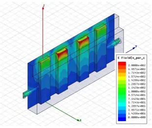
4.2.3 E-Field 26
4.2.4 H-Field 27
4.2.5 Surface Current 27
4.3 Conclusion 28
5 CONCLUSION AND RECOMMENDATION 29
5.1 Conclusion 29
xi
xii
LIST OF FIGURES
FIGURE TITLE PAGE
1 3-Dimensional of waveguide 8
2 Basic structure of SIW 9
3 Diameter and Pitch 10
4 Flow chart 13
5 Option in CST Studio Suite and RF antennas selected 14 6 Waveguide selected 15
7 Work plane in CST 15
8 SIW and equivalent rectangular waveguide 19
9 Topology of an SIW guide realized on a dielectric substrate with its physical dimensions 20
10 Design of filter 21
11 Parametric studies for return loss 23
12 Parametric studies for bandpass 23
13 Return loss 24
14 Bandwidth 24
15 Insertion loss 25
16 E-field 26
17 H-field 26
xiii
LIST OF TABLES
TABLE TITLE PAGE
1.1 Summarize Journals 5 1.2 The design characteristic of the filter 16 1.3 Design specification of SIW filter 16
1
CHAPTER 1
INTRODUCTION
This chapter will explain about the project briefing, problem statement, objective and scope of work.
1.1 Project Briefing
2
1.2 Problem Statement
The main problem in RF Front-End is gain (to change over the generally weak signals to advantageous sufficiency levels for further handling) and frequency conversion (to change over signals to helpful frequencies for further processing). In the get way, choosing the desired channel among (numerous) different channels, and extricating the data that is connected through modulation to the radio flag, is
normally done in the IF signal processing circuits. In the transmit way, regulating the data to be transmitted onto a radio flag is regularly additionally done in the IF
circuits [3]. Other problem is high traffic spectrum, congested capacity and fully utilize. Increasing the number of tension of wireless communication frequency resources, requires an upgraded as developing modern microwave and millimeter wave components. With these problems could give a bad communication frequency and transmission. Jamming of sending data or signal could happened too. To solve the problem is by choosing the millimeter wave which have a high speed, high bandwidth and high capacity. By applying the millimeter wave could give a better frequency and transmission. So that, 28GHz is chosen as candidate. Next, focus on rectangular waveguide filter to be modified as SIW. Because of rectangular too bulky and costly, need to be modified to a low cost and easy to integrate.
1.3 Objective
The objective of this project is to design a millimeter wave filter that utilize substrate integrated waveguide band pass filter operates at 28GHz. This filter design is able to achieve a low insertion loss and good selectivity because of the Q factor of SIW is high, as result it will produce high performance filters. Measurement data also take part for obtained a good performance.
1.4 Scope of Work
3
simulation and measurement. Then, the result will be compared with the
measurement result and the actual results. Other S-parameter such as return loss level, insertion loss, and structure will also be focus at as to know performance of filter design.
1.5 Organization of Thesis
In chapter 2, present the researched journals that were reviewed about the filter design at varies frequency. After choosing the desired journals by changing the exact frequency which is at 28GHz, comparison was carried among them. An addition this chapter covers a detail theory about a filter and its parameters that determine its performance.
In chapter 3, will explain about the method and flow of designing for this project from the beginning until the end of the project.
In chapter 4, briefly explain the result of the filter design for millimeter wave filter RF Front-End Transceiver that are obtained through simulation. The simulation result of the filter was obtained using CST Studio Suite 2016.
4
CHAPTER 2
LITERATURE REVIEW
This chapter present the researched journals that were reviewed about the filter design at varies frequency. After choosing the desired journals by changing the exact frequency which is at 28GHz, comparison was carried among them. An addition this chapter covers a detail theory about a filter and its parameters that determine its performance.
2.1 Critical Literature Review
The literature review was performed on a journal to collect related information and facts that can be used in the design process of this project
5
2.1.1 Summarize Journals
Using a general mode-matching technique, gives 3.4 dB insertion loss and 17 dB return loss over the whole passband at near 24 GHz (K-band) with 440-MHz bandwidth (1.8%) [4].
Mode-matching techniques (MMTs) are employed to facilitate the design of planar SIW circuits as well as surface mounted waveguide (SMW) components. Active component integration and antenna design employ commercially available field solvers [5].
Novel compact millimeter wave bandpass microstrip filter using a three-mode resonator with two shunt stepped impedance open stubs. The simulated insertion loss S 21 is less than 1.2dB, and the return loss is greater than -17.3dB in the passband. Moreover, the attenuation below -20dB is from 42 to 90GHz [6].
Tapered fin-line transition is designed for dielectric substrate having a relative permittivity higher than 4. Measurement results of a back-to-back transition show excellent performance in a bandwidth of 6% (33-35 GHz) with less than 1 dB of insertion loss and a return loss of better than 15 dB [7].
Using irises inside a rectangular hollow waveguide we can design wide bandwidth filter to cover the whole 40-60 GHz frequency range [8].
A millimeter wave wideband bandpass filter is proposed and designed by using novel slotted substrate integrated waveguide (SIW) units. The unit consists of two pairs of same size dumbbell slots etched on both the top and bottom metal planes of the SIW. The slots act as shunt resonators, which reduce the filter size and
produce transmission zeros simultaneously. A five-order bandpass with a center frequency of 32.5 GHz and a 3dB fractional bandwidth of 34.6% is developed, and it is small in size, and low loss with a measured insertion loss of 1.54 dB at the center frequency [9].
6
Table 1.1: Summarize Journals
Journal Application Method Improvement
[4] K-band at
26.5GHz Mode-matching technique (MMTs) The expected result achieved for return loss and cross polarization [5] Microstrip filter at
42GHz to 90GHz Three-mode resonator (two shunt stepped impedance open stub) Enhance the insertion loss, attenuation and return loss
[6] W-band at 90GHz
to 98GHz SIW Chebyshev filter inductive cross-shaped metal
Good achieved of BW at central frequency, low pass band
insertion loss and a high stop band insertion loss
[7] SIW at 33GHz to
35GHz Antipodal fin-line Reduce of insertion loss and a better of return loss. BW is 6%
[8] Wide pass-band at
40GHz to 60GHz Irises rectangular waveguide Enhance the insertion loss and return loss
[9] Wideband
bandpass at 20GHz to 40GHz
Novel slotted SIW Reduce filter size and produce transmission zeros. Achieved good BW
[10] Microstrip at
40GHz to 80GHz Novel tunable band gap filter Different parameters as tunable. Achieved for BW, return loss and insertion loss
2.2 Filter Theory
7
day is expelling a few frequencies and not others with a specific end goal to suppress interfering signals and lessen background noise.
2.3 Filter Properties
There are many of basic properties that are used to describe the performance of the filter. There are including insertion loss, return loss and bandwidth.
2.3.1 Insertion Loss
Insertion loss is defined as a ratio of the signal level in a test configuration without the filter installed (|V1|) to the signal level with the filter installed (|V2|). This ratio is described in dB by the following equation (2.1);
(2.1)
Where;
IL = Insertion loss
(|V1|) = without the filter installed
(|V2|) = with the filter installed
|V2| < |V1| IL is positive and measures how much smaller the signal is after adding the filter.
In case the two measurements ports use the same reference impedance, the insertion loss (IL) is defined as equation (2.2);
8
2.3.2 Return Loss
Return loss is an advantageous approach to portray the input and output signal sources. Return misfortune can be characterized in dB as in the following equation (2.3);
(2.3)
Where;
RL = Return loss
Г = Reflection coefficient
2.3.3 Bandwidth
Bandwidth is the difference between the upper and lower frequencies. In other words, range of frequency that the filter specification may require that within the filter passband. The 3dB bandwidth of an electronic filter is the part of the system‟s frequency response that lies within 3dB of the response at its peak, which if the filter may operate is at or near its centre frequency.
The bandwidth can be the scope of frequencies on either side of the centre frequency where the filter qualities like maximum and minimum gain and input impedance which have obtained at the centre frequency.
2.4 Rectangular Waveguide
Rectangular waveguides are the one of the earliest type of the transmission lines. They are used in many applications. A lot of components like isolators, attenuators, couplers and slotted lines are available for various standard waveguide bands between 1GHz to above 220GHz.
9
In most of communication system, metallic waveguide plays essential part in satellite communication framework and are regularly utilized between high power amplifier and transmitting antenna to acquire great coordinating. In this way, waveguide filters in millimeter band have been utilized as a part of numerous applications than
stripline filters. There are some factors why waveguide is a good candidate compared to stripline because of their low loss, high quality factor, and high power capability [11]. There are some disadvantages which is its too bulky and costly.
[image:22.595.164.475.340.603.2]Waveguide may be designed in many ways of methods until the substrate integrated waveguide were used to get a better performance and low cost of filter. It is one of the most popular filter for the production of low radiation loss, low insertion loss and high Q [4]. Figure 1 shown the 3-Dimensional of waveguide.
10
2.5 Substrate Integrated Waveguide
Substrate Integrated Waveguide (SIW) is a development in recent years, dynamic gadgets and detached segments can be coordinated high-productivity, and the measure of microwave and millimeter wave framework is diminished effectively. Besides, its mass-producible, elite and high return microwave. At millimeter wave frequencies, specifically, circuit-building squares including antenna components are firmly identified with each other through electromagnetic couplings and
interconnect.
At present, the SIW method has a wide range in many microwave gadgets
application, such as filters, power dividers, directional couplers, antennas, oscillators, power amplifiers, power selective surfaces and etc. This shown that SIW is a good technique to obtain better performance and at the same time may reduce the cost of material. The field distribution in an SIW is similar to that in a conventional metallic waveguide [12].
[image:23.595.134.527.481.600.2]Substrate integrated waveguide in its fundamental shape comprises of 4 sections (dielectric substrate, diameter and pitch) as appeared in Figure 2. Where L is the length of SIW cavity, W is the width of SIW cavity, h is the dielectric substrate thickness and εᵣ substrate relative permittivity.
11
2.5.1 Dielectric Substrate
Between the top and bottom metal planes of substrate it is the dielectric layer. There are a great deal of substrate material and particulars to look over as indicated by the receiving filter necessity. The most two elements determining dielectric substrate will be substrate height (0.003 λo ≤ h 0.05 λo) and dielectric constant (2.2 ≤ εᵣ ≤ 12).
Substrates that are thick with low dielectric constant are preferable for enhancing efficiency, bandwidth and radiation in space. On the other hand substrates that are preferable for microwave circuits should be thin with high dielectric constant.
2.5.2 Diameter and Pitch
Diameter and pitch otherwise called distance between focal point to focal point of via hole appeared in Figure 3.
[image:24.595.237.407.411.516.2]With a specific end goal to limit the leakage loss between nearby hole, pitch should be kept as little as could be expected under the circumstances.

![Figure 2: Basic structure of SIW [4]](https://thumb-us.123doks.com/thumbv2/123dok_us/71647.6722/23.595.134.527.481.600/figure-basic-structure-of-siw.webp)
![Figure 3: Diameter and Pitch [4]](https://thumb-us.123doks.com/thumbv2/123dok_us/71647.6722/24.595.237.407.411.516/figure-diameter-and-pitch.webp)
