On the Implementation of a Low-Power IEEE 802.11a Compliant Viterbi
Decoder
K. Maharatna
!, A. Troya*, M. Krstic** and E. Grass**
!
University of Bristol, UK, *Infineon Technology, Germany, ** IHP, Germany
[email protected]
,
[email protected]
, {krstic,
grass}@ihp-microelectronics.com
Abstract
This article describes a standard cell based novel implementation of a low-power Viterbi Decoder (VD) targeted for the IEEE 802.11a Wireless LAN system. Multiple clock rates have been used to reduce the power consumption and the inherent bandwidth mismatch between the Add-Compare-Select (ACS) and traceback operations. Aggressive clock gating and innovative circuit techniques reduce the power consumption further. The normalized cell area and dynamic power consumption of the designed VD are 5.9 mm2
and 53 mW respectively. The normalized power dissipation of the VD is 0.66 mW / Mbps.
1. Introduction
Orthogonal Frequency Division Multiplexing (OFDM) based IEEE 802.11a WLAN system targeting a data rate of 6 – 54 Mbps using BPSK, QPSK and QAM modulation schemes [1] is currently the focus of research and development. One prime implicit constraint for the development of such a system is to reduce the overall power consumption. This requires optimized design of the most computationally intensive components. Recent studies show that the 64-state Viterbi Decoder (VD) is the most computationally intensive part at the receiver of such a system [2]. The timing requirement for such a system can be satisfied using a VD that can operate at a speed of 80 Mbps [2]. However, design of such a large-state high-speed and low-power VD is a challenging task. The present article addresses the design issues concerning such a VD.
Although several techniques for designing VD have been developed in the past adaptation of those in the present case either leads to significantly high hardware complexity (and hence significant power consumption) or slower operation speed. Also, to reduce the power consumption, often manipulations in the transistor
level are needed for performance critical blocks. This approach is not suitable for standard cell based designs. In this article, we present a purely standard cell based novel design of a low-power VD for IEEE 802.11a WLAN applications that exploits the inherent bandwidth disparity of the ACS and traceback operation as a natural clock partitioning boundary. Since the technology at hand is a standard cell CMOS technology, we have concentrated only on the power reduction in the architectural level. For this purpose clock gating has been used aggressively. Also, the technology library at hand does not contain appropriate memory modules and thus we had to use register-based memory structure which understandably occupies more silicon area and consumes more power compared to its proper memory-based counterpart. However, despite those limitations, the VD proposed here occupies moderate area and consumes only 53 mW power at 80 MHz frequency. The rest of the paper is structured as follows: a discussion on the design parameters in the present case is provided in Section 2 and the proposed architecture is described in Section 3. Section 4 discusses the implementation results. Conclusions are drawn in Section 5.
2. Design parameters
introduced by the datapath processing. By accounting for this, L = 24 for the signal field and a minimum value of L = 40 for the data field seems to be a reasonable compromise between the hardware requirement and noise performance. However, the fact that there is only marginal performance degradation for L in the range of 35 to 50 has been used efficiently in our design to satisfy the specified throughput rate which will become clear in the forthcoming sections. 16-level input quantization has been used in our design since a further increase of the quantization level is known to lead to little improvement of performance. On the other hand reduction of level of quantization results in loss of accuracy.
From the operation point of view, the VD needs to decode the signal field of the data frame first. The decoded signal field gives the information about the appropriate configuration of the demodulator and the number of OFDM symbols being transmitted. At the end of the entire transmission frame, one needs to flash out the datapath of the VD completely. Considering the requirement of the above mentioned functionalities, it can be seen that the control mechanism of the target VD is not a trivial one. It should be capable of decoding the signal field completely even before arrival of the data field and has to initiate an internal flash out operation immediately after decoding the signal field. On top of that it should be capable of detecting the end of the frame using information of the decoded signal field and flash out the data before a new frame begins.
3. Architecture
The block diagram of the proposed VD architecture is shown in Figure 1. It consists of the Branch Metric Unit (BMU), ACS and traceback unit as the principal functional blocks. The additional blocks FIFO and G_MIN are a temporary storage and the global minima selection unit respectively. The traceback unit is further divided into two parts viz. Traceback Memory (TBM) and Traceback Logic (TBL).
In principle, the minimum size of the traceback memory unit required in the present case is 64×L. However, in order to use this minimum memory, L traceback operations have to be executed before obtaining a single decoded output. This approach can only be applied to a low-speed VD as there is a 1:L bandwidth mismatch between the input data rate and the traceback operation. To achieve 80 Mbps decode rate the memory access rate has to be as high as 80L MHz. The high ratio of memory access rate to the decode rate is extremely difficult to meet. The architecture proposed here solves the problem by conceptually separating the traceback mechanism from
[image:2.612.321.538.334.428.2]the remainder of the VD functionality using two distinct clock domains viz. 10 and 80 MHz respectively (shown in Figure 1) and outputting a corrected ‘byte’ instead of a single bit. This arrangement maintains the required output data rate and at the same time reduces the imbalance between the input data rate and the traceback operation. However, since the minimum traceback length required in this case is L the total memory required is of length L + 8. Thus, in our case, the actual memory used for the signal field and the data field decoding are of length 32 and 48 respectively. As has been discussed in Section 2 this arrangement does not incur any performance degradation since the minimum value of traceback length for the respective cases are always obeyed. An additional advantage of this strategy is that since the time constraint for memory access rate is greatly relaxed, the dynamic power saving is potentially significant. Like the traceback unit, the G_MIN unit is also divided into two sub-units, viz., G_MIN1 and G_MIN2. This arrangement is done from timing and power consumption point of view.
Figure 1. Proposed architecture of the VD
In principle the VD runs in three modes namely, decoding of signal field, decoding of normal data field and decoding of the last data of the data frame. Three different signals sig, start_vit and last_data respectively have been provided at the primary input of the VD to distinguish each of these cases. These signals have been used to internally encode the operation sequences of the VD in the form of a 2-bit signal mode (00 • normal operation, 01 • signal field operation and 11 • flash out operation) which is used efficiently to control different modules of the VD.
the modules can be viewed as a self-sufficient block, which can be activated by an external enable signal. These enable signals have been used to gate the clock for a particular module and thereby reducing unwanted power dissipation. In principle, the maximum power saving can be achieved for the register-rich modules like FIFO and TBM since unwanted clock activities at the inputs of the register-rich modules cause significant power dissipation. In addition to that, when the data flows through different modules, at every clock cycle the mode signal corresponding to that data (i. e., whether the present data is the data in signal field or normal data or the last data) also flows through the modules in the same manner. This is often termed as a “token flow” strategy where the information of the mode signal can be used to invoke appropriate type of operation on the data. The detailed architectural descriptions of the different modules are provided in the forthcoming subsections.
A. BMU
In our implementation we have used Euclidian distance to compute the branch metric. Signed antipodal values have been used to reduce the complexity further. This formulation means that the branch metrics can be calculated using simple addition and subtraction of the received bits. The BMU receives a pair of 4-bit soft inputs and computes the corresponding branch metrics. It consists of two adder/subractors and generates four outputs which are used in the ACS unit. We found that a Ripple-Carry-Adder (RCA) configuration is sufficient to satisfy the 80 MHz clock frequency. Considering the above mentioned formulation of the branch metric; in our implementation the ACS unit requires the sum, difference, negated sum and negated difference of the input soft bits. Therefore, to avoid the possibility of repeated logic in the ACS unit, these functionalities are absorbed into the BMU, which provides all four values in its interface with the ACS unit.
B. ACS
The ACS unit is responsible for recursive computation of the path metric. In the present case depending upon the operation on the BMU data, we have identified four unique types of butterfly like flowgraph showing the relationship between the predecessor and successor states. This property has been exploited by grouping appropriate states together to reduce the number and length of global wires. Each butterfly unit computes two path metrics and two decision bits (choice of shortest path) corresponding to two states. 32 such modules have been used to realize fully parallel 64-state ACS operation. Modulo-2 arithmetic has been used for automatic normalization of the path metric [4]. Our simulation shows that the
[image:3.612.322.532.121.265.2]upper bound of the differences of path metrics is 176. Thus, the required width of the path metric register for modulo-2 normalization is 9 bits.
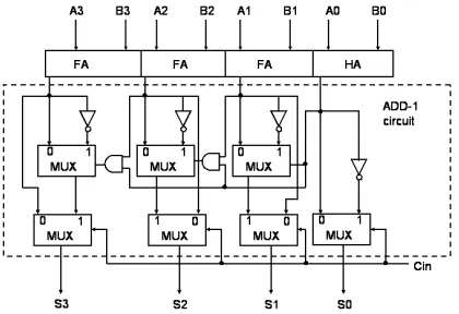
Figure 2.The proposed CSA structure
The main arithmetic datapath component for the ACS unit is adder/subtractor and the worst case delay is determined by the time of addition/subtraction of two adders: one adding a 5-bit number with a 9-bit number and another subtracting two 9-bit numbers. In order to enhance the speed of this unit we have employed the Carry-Select Addition (CSA) scheme in conjunction with the concept presented in [5] where the sum corresponding to the input carry = ‘1’ can be computed from the sum considering ‘0’ input carry using an add-1 circuit. This enables one to implement a high-speed adder circuit without significant hardware overhead. But the add-1 circuit proposed in [5] cannot be applied to a standard cell-based design since manipulation in the transistor level is required. In our design we have used a new modified add-1 circuit based on the standard logic gates. Fig. 2 shows the circuit diagram of a 4-bit CSA as an example. The resultant circuit is slightly slower than the conventional CSA by one AND gate and a 2-to-1 multiplexer delay but cuts down the hardware significantly. The chosen configuration for the adder is 5-4, which approximately needs hardware equivalent to a 6-bit RCA. On the other hand we have used 2-3-4 configuration for the 9-bit subtractor. The worst case delay for the first adder is approximately equal to 5 × Ta, assuming the sum of
delay of the multiplexer and a half adder equals to one full adder delay and Ta being the delay of one full
adder. The worst case delay for the subtractor under the same simplified consideration can once again be given approximately by 5 × Ta. Thus the worst case
delay of the entire circuit can be given by 10 × Ta,
Like the BMU, the control of the ACS unit is simple. It provides enable signal to the FIFO module (fifo_enable) According to the operation sequence, the FIFO module in general follows the ACS unit. Thus, the signal fifo_enable can be generated by delaying the acs_enable signal through a register. The clock gating inside the ACS unit is done by logical ANDing of the clock with the acs_enable signal.
C. FIFO
In our implementation, the fact that the traceback unit and the ACS unit run at 10 and 80 MHz respectively calls for buffering of decision bits emerging from the ACS unit for eight cycles. A FIFO block of size 64×8-bits stores the decision bits coming from the ACS for eight clock cycles and then transfers the data as a chunk to the main TBM unit. Unfortunately since our library does not contain optimized RAM module we have used only registers to design this unit. In order to find out the optimum configuration using conventional registers, three different configurations and their impact on area and power of the architecture is explored. The configurations are: a conventional FIFO memory using shift register (FIFO_SR), a ring buffer-based FIFO architecture (FIFO_RB) and a ring buffer-based FIFO architecture with the pointer operation encoded using gray code (FIFO_RBG). The synthesis result in our library shows that FIFO_RBG offers 6.5% power reduction at the expense of 0.3% area over the FIFO_SR configuration which is not a significant advantage owing to the small size of the FIFO block. The performance of FIFO_RB falls in-between the performance of FIFO_RGB and FIFO_SR configurations. However, the small power saving of the ring buffer-based architectures is likely to be lost at the layout level owing to its requirement of long routing wires and subsequent additional capacitance and resistance. On the other hand, FIFO_SR can be implemented using only local connections and thus is expected to offer a better power performance at the layout level. Taking this fact into account we have selected FIFO_SR structure for implementing the FIFO block.
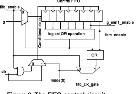
Compared to the control structures of BMU and ACS, the control of FIFO block is more complex. In principle, the FIFO block can operate in two modes: the normal mode and the flash mode. The flash mode corresponds to the situations of decoding the signal field and the last data. In both the cases one needs to clock the circuit until the final data transfer to the TBM occurs even if the fifo_enable signal is de-asserted whereas, in the normal mode of operation, the unit ceases to work as soon as the fifo_enable signal is de-asserted. The control circuit required to satisfy this
functionality is shown in Figure 3. Its main component is a control FIFO of length eight. When the first data from the ACS unit arrives at the 0th
64 × 1 bit register of the FIFO block the signal fifo_enable is passed to the leftmost register of the control FIFO through the multiplexer shown in Figure 3. This logic ‘1’ is propagated through the control FIFO at successive clock cycles whereas; logic ‘0’ is inputted at the leftmost register of the control FIFO at successive clock cycles. Thus, the logic ‘1’ in the control FIFO in principle ‘tracks’ the data wavefront in the FIFO memory block. Once this logic ‘1’ reaches the rightmost register of the control FIFO, it serves as the enable signal for the TBM unit (tbm_enable). In the next clock cycle the data transfer from the FIFO to the TBM unit occurs and the tbm_enable signal is automatically de-asserted as can be seen from Figure 3. After data transfer the leftmost control FIFO is once again loaded with the logic value of fifo_enable signal and the operation continues. It can also be noted from Figure 3 that the enable signal for G_MIN1 unit (g_min1_enable) can be derived by taking the output from the 6th
position of this control FIFO. Generation of the gated clock (fifo_clk_gate signal) has also been shown in Figure 3. It has to be noted that under normal mode of operation if the signal fifo_enable is asserted low then the entire module gets frozen in its current state. In order to achieve that it is necessary to apply a ‘conditional clock’ to the control FIFO which is also shown in Figure 3.
D. G_MIN
The G_MIN unit detects the global minima position of the path metric at a given time from where the traceback operation starts. From the operational point of view, it evaluates the global minima at every 8th clock cycle and has only two clock cycles for this evaluation so that the traceback operation can start at the correct time. To shorten the critical path and to provide a better control over power reduction through clock gating we have physically divided the G_MIN unit in two parts viz. G_MIN1 and G_MIN2 and thereby introducing single stage pipelining in the G_MIN unit. G_MIN1 and G_MIN2 are configured as 32-16-8 and 4-2-1 tree structure of subtractors respectively. Each of the subtractors has been designed using the modified CSA described earlier. The configurations used here is 2-3-4. Thus the delay of the basic subtractor becomes approximately equal to 5 × Ta.
units has been done by logical ANDing of the clock with their respective enable signals. It can be noted that a significant power saving may result with this arrangement since the G_MIN1 and G_MIN2 sub-blocks are active once every 8th clock cycle and also not at the same time but at the successive clock cycles.
Figure 3.The FIFO control circuit
E. Traceback Unit (TBM & TBL)
The traceback unit consists of TBM and TBL sub units. Our use of the traceback algorithm to output a byte instead of a single bit necessitates adaptation of the TBM typically used in a VD. We also need to provide the necessary flexibility for reverting to a 24 length traceback operation for decoding of the signal field. Therefore, the TBM has been implemented as 6 memory sub modules of 64×8 bits, a total of 64×48 bits. When tbm_enable signal is high the 64×8 data residing in ith
sub module is shifted to the (i• 1)th
sub module, where i∈{5, …, 1}. At the same time, i = 5 sub module receives its data from the FIFO block. Each of the memory sub modules is provided with a gated clock to minimize power consumption.
To control the operation of the TBM unit a 6-bit counter has been used. The main purpose of this counter is to track the data inside the TBM unit. The counter is incremented by eight whenever the signal tbm_enable is high. As mentioned earlier, during decoding of the signal field we have selected a traceback length of 24. Since we generate eight output bits in one go, the effective traceback length for each of the bits varies between 24 and 32 (32 for the oldest bit and 24 for the most recent bit). To achieve this it is sufficient to use four memory sub-modules only whereas the other two sub-modules of the TBM unit can be turned off by gating the clock. The counter output in conjunction with the mode signal is used to gate the clock for those sub-modules. The flash-out operation during the signal field decode requires continuation of clock transition at the active memory
sub-modules even after de-assertion of the signal sig. This is ensured by the counter which keeps track of the number of data residing inside the TBM unit. With every data byte output, the value of the counter is decremented by 8 until zero is reached. At this point all the data has been flashed-out from the TBM unit. The control philosophy adopted for decoding the last data symbol is more or less the same except that in this case all the memory sub-modules are in active state. Since the counter is incremented by eight when tbm_enable is ‘high’, in the normal operation mode a steady state for decoding (TBM unit full, decoding start) is reached when the value of the counter reaches to 48. At this particular point the counter is ‘frozen’ as long as the steady state computation persists, i. e., after every eight clock cycles a corrected byte is outputted and at the same time eight 64-survivor bits for the most recent inputs are copied to the TBM from the FIFO. Once the last 64-survivor bits are copied to the TMB, the operation enters into the flash-out mode (last data case) where with every data byte output; the counter is decremented by eight until it reaches to zero. The entire control circuit for this block has been synthesized from the behavioral description coded in VHDL.
The traceback operation starts from the index position detected by the G_MIN circuit as the global minima position. The entire traceback operation can easily be expressed in terms of multiplexers. Thus, the TBL unit is implemented using a long chain of multiplexers. Since the traceback operation runs at 10 MHz clock frequency the timing constraints are relaxed enough to accommodate the long critical path of such a circuit.
4. Synthesis and Implementation
The proposed VD has been tested as a ‘stand-alone’ block and also ‘in system’, where it has been integrated in an experimental baseband chip for IEEE 802.11a WLAN modem. In the ‘stand-alone’ case input data for each of the modulation scheme has been generated using Matlab simulation and then applied to the VD through VHDL test bench and the output is checked against Matlab simulation output. In all the cases it was found that the VD works correctly. The ‘in-system’ testing is done for all the specified modulation schemes for different data rates. The input data used for the testing are the example data given in the standard specification [1]. In all the cases it has been found the system performs correct operation with the designed VD.
analyzed using Synopsys’ Prime power. First the activity file has been derived from Modelsim and then this activity file has been used in Prime power to compute the power consumption of different modules.
[image:6.612.75.294.239.324.2]The synthesized cell area of the VD is 5.9 mm2. The ACS unit occupies the majority of the area of the design (44%) followed by the TBM unit (33%). This is mainly because of register-based approach since suitable memory cells was unavailable. The G_MIN unit (total 10%) and the combinatorial logic of the TBL (nearly equal to 6.6%) are the next biggest, closely followed by the BMU that occupies 0.3% of the total system.
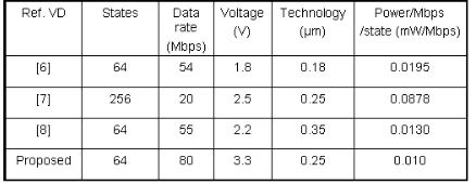
Table 1.Power performance comparison of the proposed VD with some other existing VD
Power consumption of the proposed VD has been analyzed “in system” using Prime Power. Inside the system the VD dissipates 53 mW power. Thus, the normalized power dissipation of the VD is 0.66mW/Mbps. The ACS unit accounts for maximum of the total power budget (48%) followed by the TBM unit (31%). Clocking of the TBM at 1/8th
rate of the ACS clock frequency results in a dynamic power saving by 87% compared to clocking it at 80 MHz. The rest of the modules altogether contribute less than 20% of the total power consumption of the complete VD. Table 1 shows power performance comparison of the propsed VD with some other existing VD. It is to be noted that different VD are intended for different applications and utilized different technologies. Thus a direct comparison of them is not a fair indication of the architectural quality. However we have used the index power/Mbps/state to give a partial impression of their power performance. A more rigorous comparison would need proper technology scaling which is difficult to do and thus is not considered here.
5. Conclusions
In this paper we presented a fully standard cell based low-power design of VD compliant with the IEEE 802.11a WLAN specification. The inherent bandwidth mismatch between the ACS operation and traceback has been minimized using two distinct clock domains. Clock gating and multiple clock domain
design strategies adopted here in conjunction with innovative circuit technique have been found profitable as far as the power consumption of the VD is concerned. However use of optimized memory modules for FIFO and TBM can bring down the power and area significantly.
References
[1] IEEE P802.11a/D7.0, “Part 11: Wireless LAN Medium
Access Control (MAC) and Physical Layer (PHY) specifications: High speed physical layer in the 5 GHz band”.
[2] E. Grass et al., “On the Single Chip Implementation of a
Hiperlan/2 and IEEE802.11a Capable Modem”, IEEE
Personal Communication, vol. 8, no. 6, pp. 48 – 57,
December 2001.
[3] Alfonso Troya, Synchronization and Channel Estimation in OFDM: Algorithms for Efficient Implementation of WLAN Systems, Ph.D. Dissertation, BTU Cottbus Germany, January 2004.
[4] A. P. Hekstra, “An alternative to metric rescaling in Viterbi decoder”, IEEE Trnas. Communication, vol. 37, no. 11, pp. 1220 – 1222, Nov. 1989.
[5] T. Y. Chang and M. J. Hsiao, “Carry-select adder using single ripple-carry adder”, Electronics Letters, vol. 34, no. 22, pp. 2101 – 2103, October 1998.
[6] C. C. Lin, Y. H. Shih, H. C. Chang and C. Y. Lee, “Design of a power reduction Viterbi decoder for WLAN application”, IEEE Trans.Circuits and Syst. – I , vol. 52, no. 6, pp. 1148 – 1156, June 2005.
[7] http://www.sigda.org/Archives/ProceedingArchives