This is a repository copy of The interface of a-SiNx:H and Si: Linking the nano-scale structure to passivation quality.
White Rose Research Online URL for this paper: http://eprints.whiterose.ac.uk/97831/
Article:
Lamers, M., Hintzsche, L.E., Butler, K.T. et al. (7 more authors) (2014) The interface of a-SiNx:H and Si: Linking the nano-scale structure to passivation quality. Solar Energy Materials and Solar Cells, 120 (Part A). pp. 311-316. ISSN 0927-0248
https://doi.org/10.1016/j.solmat.2013.04.026
Article available under the terms of the CC-BY-NC-ND licence (https://creativecommons.org/licenses/by-nc-nd/4.0/)
[email protected] https://eprints.whiterose.ac.uk/
Reuse
This article is distributed under the terms of the Creative Commons Attribution-NonCommercial-NoDerivs (CC BY-NC-ND) licence. This licence only allows you to download this work and share it with others as long as you credit the authors, but you can’t change the article in any way or use it commercially. More
information and the full terms of the licence here: https://creativecommons.org/licenses/
Takedown
If you consider content in White Rose Research Online to be in breach of UK law, please notify us by
The Interface of a-SIN
x:H and SI: Linking the nano-scale
structure to passivation quality
Machteld Lamers1, Leif E. Hintzsche2, Keith T. Butler3, Per Erik Vullum4, Chang-Ming Fang2, Martijn Marsman2, Gerald Jordan2, John H. Harding3¸ Georg Kresse2 and Arthur Weeber1
1 ECN Solar Energy, P.O. Box 1, 1755 ZG Petten, the Netherlands, Phone: +31 88 515 56 4718, Fax: + 31 88 515 8214, E-Mail: [email protected].
2 University of Vienna, Faculty of Physics and Center for Computational Materials Science, Sensengasse 8/12, A-1090 Vienna, Austria.
3 University of Sheffield, Western Bank, Sheffield S10 2TN, United Kingdom.
4 SINTEF, Materials and Chemistry, Box 4760 Sluppen, NO-7465 Trondheim, Norway.
Abstract
Surface passivation by hydrogenated amorphous silicon nitride (a-SiNx:H) is
determined by the combined effect of two mechanisms: so-called chemical passivation by reducing the density of interface states (Dit) and field-effect passivation as a result of the
number of fixed charges (Qf) at the interface with Si. These are related to the K defect
centre: *Si N3. Defects near the interface (in both Si as in a-SiNx:H), modelled by force
field Molecular Dynamics (MD) and ab initio Density Functional Theory (DFT), can be related to Qf and Dit measured experimentally using CV-MIS (Capacitance-Voltage Metal
Insulator Semiconductor). The compositional build up at the interface as is determined by HRTEM (High Resolution Transmission Electron Microscopy) and modelled by MD correspond to each other; a gradual change from Si to the bulk a-SiNx:H composition in the
first 2 nm of the a-SiNx:H layer. At the c-Si side a highly distorted layer (about 1-3 nm)
caused by the insertion of N and/or H is found. The insertion and adhesion of N into and at the Si surface is called nitridation and can be altered by using a NH3 plasma prior to
a-SiNx:H deposition. HRTEM image analysis shows that by varying the nitridation of the Si
surface the amount and penetration depth of N inside the Si surface is altered. Using MD modeling, it is shown that this process changes the amount of K-centers at the surface, which explains the variation in Qf and Dit that is found experimentally. Ab initio DFT
studies of a-SiNx:H (x=1.17) show that K-centers and Si atoms in distorted configuration,
are the dominating defects resulting in a higher Dit. For lower x (x=1) the Dit caused by
K-centers increases, which is observed experimentally too.
Keywords: Silicon Nitride; passivation; interface; nitridation; fixed charge
1.
Introduction
Hydrogenated amorphous silicon nitride (a-SiNx:H) is the standard antireflection and
passivating layer, for both surface and bulk defects, in wafer-based silicon solar cells. The passivating properties of the layer have previously been correlated to cell output properties like the open-circuit voltage Voc [1,2]. The total surface passivation is determined by the
combined effect of two mechanisms: so-called chemical passivation by reducing the density of interface states (Dit) and field-effect passivation as a result of the number of
fixed charges (Qf) at the interface with Si. A low Dit reduces the recombination rate at the
interface. For Qf the effect on surface passivation depends, besides other parameters, on
a-SiNx:H/Si, this indicates that they are determined by the initial growth of the a-SiNx:H
layer. The relationship between Qf, Dit and the a-SiNx:H layer properties are published
elsewhere by the authors [4]. Qf is related to the interface structure between the materials
(a-SiNx:H and Si) causing a local-field effect as was described by Aspnes [5]. This local
field depends on the different polarizabilities of each material and the variation in volume density of these polarizabilities over a certain distance at the interface. The different components in bulk a-SiNx:H, which can be charged have been linked to the so-called K-
and N-centers [6]. These centers are respectively *Si N3 and *N=Si2. * indicates that these
centers can be neutral, positive, negative or bonded to H. Assuming that K- and N-centers also occur at the interface, this leads to the conclusion that Qf is determined by the
variation and volume fractions of K- and N-centers at the interface region of a-SiNx:H/Si.
In this paper our aim is to better understand the surface passivating properties by examining the interface both on electrical and physical properties, and comparing the results to force field Molecular Dynamics (MD) and ab initio Density Functional Theory modeling. We show that the compositional build up at the interface as is measured and modelled correspond to each other; a gradual change from Si to the bulk a-SiNx:H
composition in the first 2 nm of the a-SiNx:H layer. At the c-Si side a highly distorted layer
(about 1-3 nm) caused by the insertion of N and/or H is found. The insertion and adhesion of N into and at the Si surface is called nitridation and can be altered by using a NH3
plasma prior to a-SiNx:H deposition. We show by High Resolution Transmission Electron
Microscopic (HRTEM) image analysis that by varying the nitridation of the Si surface the amount and penetration depth of N inside the Si surface is altered. Using MD modeling, we show that this process changes the amount of K-centers at the surface, which explains the variation in Qf and Dit that is found experimentally. Furthermore, with ab initio
modeling we show that a large amount of H is present at the surface, needed to passivate the dangling Si bonds. Even more, we propose that the location of Qf is stretched over the
interface, starting a few nm in the c-Si to around 2 nm in the a-SiNx:H, the magnitude can
be altered by changing the concentration gradient, more specifically of N in the c-Si. This can be achieved by using a NH3 plasma prior to a-SiNx:H deposition.
2.
Results
2.1 A graded interface
a-SiNx:H was deposited by remote Plasma Enhanced Chemical Vapour Deposition
(PECVD) on a double side mirror-polished <100> 2.5 cm p-type and <111> n-type 3.5
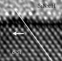
Fig 1. HRTEM image of a-SiNx:H/c-Si interface of the <100> sample.
A white line is drawn over the high amplitude periodic signal. It is observed that the first few atomic layers of c-Si at the surface show a distorted expanded crystal structure and that the high amplitude signal is shifted left and lowered in intensity. This indicates the presence of large strain and the possible insertion of other smaller atoms. A dark band is seen at the interface, which can indicate that light atoms, like N and/or H, are present. Such a dark band is not visible at a SiO2/c-Si interface [7].
Large strain was also found in the <111> oriented sample as shown in the inverse fast Fourier transformed (FT) image (figure 2c), and corresponds to the dark band in figure 2a. No such strain was found in the c-Si bulk (figure 2b).
Fig 2. a) HRTEM image of a-SiNx:H/c-Si interface of the <111> sample; b) FT image of c-Si; c) FT
image of the interface of a-SiNx:H and c-Si.
On the a-SiNx:H side of the interface a 2 nm wide gradient was found in the plasmon
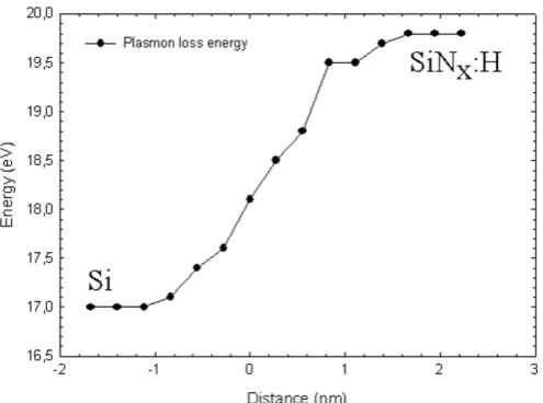
[image:4.595.188.440.502.665.2]Fig 3. The plasmon loss energy over the interface of the <100> sample.The interface is at 0 nm.
In the figure it can be seen that the plasmon loss energy increases from 17.0eV to 19.8eV over 3 nm (from -1 nm to 2nm). From the high-loss region of the EELS spectrum also the chemical composition can be determined and this is shown in figure 4. Park et al. showed a relation between the plasmon loss energy and the composition of a-SiNx:H [8]
and we find that this is also valid for the interface. The relation between plasmon loss energy and composition combined with the increase in plasmon loss energy occuring at the Si side (~1nm) indicates the presence of N inside Si, besides H. The presence of N was also found inside Si surface by Ikarashi et al. [9]. The composition is determined from the L2,3 peak onset in the high-loss region of EELS (around 99 eV) and it could not be found to
[image:5.595.190.438.83.267.2]change for t<0.5 nm; this indicates that the N content is relatively low.
Fig 4. Experimentally determined change in composition at the interface in a-SiNx:H of the <100>
sample.The interface is at 0 nm..
2.2 Nitridation, Qf, Dit and K-centers
Using remote-PECVD, the gasses to deposit a-SiNx:H, typically SiH4 and NH3, are
dissociated. Subsequently, a thin film a-SiNx:H can now grow on the substrate surface.
During the initial growth of a-SiNx:H the surface is nitridated, which can be described as N
adhesion at or insertion into the Si surface. This nitridation is temperature dependent. Typically, adhesion of -NH2 to the Si surface starts above 350°C, N insertion into the Si-Si
nitridation on passivation in more detail, NH3 plasma pre-treatments prior to a-SiNx:H
layer deposition were performed on 275 µm thick p-type FZ <100> wafers, which were double side mirror polished with a base resistivity of 2.5 cm. Shortly before nitridation, the wafers received a short HF dip to remove the surface oxide. Samples with nitridation and coating on one side were used to determine Qf and Dit using CV-MIS. CV-MIS
samples were prepared by evaporating 300 nm aluminum on the full area of the uncoated rear side and circular dots with varying sizes (0.1 – 1.91 mm2) on the coated front side. The thickness of the a-SiNx:H layers was determined using spectroscopic ellipsometry. The
method to analyze the CV-MIS curves is described in [11].
[image:6.595.186.439.249.419.2]NH3 plasma pretreatments were carried out at temperatures between 300 and 500°C. In
figure 5 the effect of the temperature of a NH3 plasma on Qf and Dit is shown [4].
Fig 5. The effect of the temperature of a NH3 plasma treatment on Qf and Dit on p-type <100>. Open and
closed symbols are samples without respectively with pre-treatment. The lines are guides to the eye [4].
A positive correlation between Qf and Dit is found. It can be seen that already at 300°C
a small effect is visible, which suggests that the onset of nitridation might start at somewhat lower temperature than suggested by Dai [10]. The nitridation effect can be seen by the increase in Qf and Dit. The relationship between nitridation, measured lifetime and
solar cell efficiency is shown elsewhere by the authors [4].
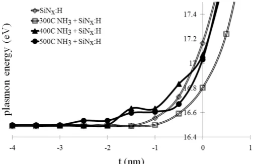
[image:6.595.188.442.570.733.2]The nitridation effect is also observed by analyzing the plasmon loss energy as was measured with an EELS line scan on the samples as is shown in figure 6.
Fig 6. Plasmon loss energy over the interface for different treatments of NH3 prior to a-SiNx:H
For NH3 treatments a rise in plasmon loss energy is found on the c-Si side of the
interface, signaling a larger incorporation of N with increasing temperature. This result is confirmed by MD simulation on graded interfaces. It shows a higher amount of N in a-SiNx:H at the interface with Si, which leads to a higher defect concentration as is shown in
figure 7. This higher defect concentration results in higher Qf. Also, the MD modeling
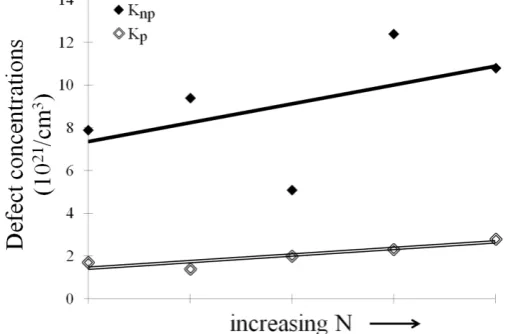
[image:7.595.186.441.215.382.2]which compares a sharp interface with a graded one, shows that gradual interfaces show significantly lower defects [12].
Fig 7. MD simulations of defect concentrations at gradual interfaces for increasing N concentration at the interface; p refers to passivated meaning the defect has a H atom bonded, np indicates non-passivated.
A clear gradient in the composition of a-SiNx:H at the interface is found and also the
presence of N is detected at the silicon side of the interface. With the NH3 plasma
pretreatment the nitridation of the Si surface is altered as shown by an increase in plasmon loss energy at the c-Si side of the interface. Experimentally, it is found that this corresponds to an increase in Qf, while MD modeling shows an increase in K-centers. The
variation in volume density of the K-centers at the interface creates a local field, which we propose is the cause of the macroscopically detected Qf. The location of Qf is stretched
over the interface, starting a few nm’s in the c-Si to around 2 nm in the a-SiNx:H.
Furthermore, Qf can be altered by changing the concentration gradient, more specifically of
N in the c-Si. This can be achieved by using a NH3 plasma prior to a-SiNx:H deposition.
2.3 Hydrogen and Dit
To increase further the understanding of the interface, ab initio density functional theory (DFT) studies for the interface of Si3N3.5H0.8 and c-Si were performed. For the
modeling 100 atoms of Si3N3.5H0.8 and 56 c-Si atoms were used. Si3N3.5H0.8 is the
configuration of the standard a-SiNx:H layer placed on the front side of solar cells, as
determined by the authors [13,14], and the orientation of the c-Si part was <111>. The amorphous structures were generated by heating the samples up to about 2500 K and then cooling them down by using two different cooling strategies. For the first strategy, the samples were cooled continuously until the systems are completely frozen. This was typically the case at a temperature of about 1500 K. Afterwards, the structure was relaxed at 0 K. About 30 interfaces structures have been obtained in this way. For the second strategy, about 500 samples were relaxed immediately at ground states. To prevent an intermixture of the c-Si and a-SiNx:H part, the degree of freedom of the c-Si atoms during
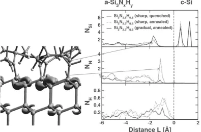
the c-Si part stayed always fixed, the c-Si atoms of the two outermost c-Si layers could either move in all directions or only in directions parallel to the interfaces. This led to systems with either gradual or sharp interfaces. Figure 8 shows the averaged concentration of Si, N, and H of quenched samples with sharp interfaces (sharp, quenched), cooled samples with sharp interfaces (sharp, annealed), and cooled samples with gradual interfaces (gradual, annealed). The figure also shows the typical bonding structures of a c-Si/a-SiNx:H interface.
Fig 8. Results of ab initio theory studies regarding the structure and concentrations at the Si3N3.5H0.8/c-Si
interface.
It can be seen that for Si3N3.5H0.8 with constant material properties a higher
concentration of N and H is found at the interface, while for a gradient interface, the interface mostly consist of H. This might explain the dark band found in the HRTEM results. In contrast to experimental measurements, no N is found in the c-Si due to placed restrictions on the atom movement during the simulations. Moreover, the dimensions of ab initio model structures are still very small compared to real systems. While the models contain about 150 atoms and cover the length scale of a few angstrom, real systems contain about 1023 atoms and demand a description at nanometer-scale. Also, initial growth of a material in a plasma cannot be modeled by ab initio methods.
In figure 9 the Density of States (DOS) of a-Si3N3.5 (x=1.17) and a-Si3N3 (x=1) are
shown. For decreasing x, the band gap shrinks, and the DOS increases due to K-centers (solid lines) and distorted Si units (broken lines) [15]. The inclusion of H decreases the density of states in the gap further (compare black and grey lines). The states caused by N-centers were found to lie outside the bandgap and we can conclude that N-centres do not have an effect on the Dit. These observations can be interpreted in several ways. It is for
example a well known fact that the optical absorption increases when the band gap shrinks. Therefore, the absorption for Si3N3 must be higher than for Si3N3.5, which is generally
known. We furthermore suppose that the number of defect states, which are mainly K-defects, are directly related to important passivation properties such as Dit and Qf. The Dit
agrees perfectly with experimental findings as shown in [4].
Fig 9. The Density of States (DOS) of Si3N3.5 and Si3N3 close to Fermi-level. The total DOS is related to
K-centers and distorted Si units (full and broken lines). Additional hydrogen (grey lines) reduces the amount of electronic defect states in the gap [15].
The observations described above correspond to the ones found experimentally on bulk a-SiNx:H. FTIR (Fourier Transform Infra Red) spectroscopy data for layers with different
composition are shown in figure 10 [4,13] and it can be seen that the concentration of distorted Si-N bonds increases for x=1 compared to the one for x=1.17. Simultaneously, the H-Si-N3 (passivated K-centers) concentration increases. These increases can be related
to higher values for Qf and Dit as shown in figure 11.
[image:9.595.187.442.554.733.2]Fig 11. Relationship between Qf, Dit and x. The lines are guides to the eye.
2.4 Effect on solar cells
The effect of NH3 plasma treatments and temperature used prior to a-SiNx:H
deposition indicate that, depending on the surface doping, a significant effect on solar cells can be expected. As the increase in plasmon loss energy in the c-Si is found to be an indication of N insertion in the c-Si surface and that this insertion is also found for surfaces without an additional NH3 plasma treatment (see figure 3), it is expected that significant
nitridation also occurs during standard a-SiNx:H deposition. Therefore, we can conclude
that both the NH3 flow and temperature used in the standard a-SiNx:H deposition will
determine the final Qf and Dit.
However, for p-type cells with highly doped n-type emitter fabricated using an NH3
plasma treatment (300-500°C) prior to front side a-SiNx:H deposition we did not observe a
difference in cell performance [4]. This indicates that these variations in surface passivation do not change the effective passivating quality of the front side for this cell design.
Contrarily, in n-type cells with a p-type emitter fabricated using NH3 plasma treatment
(300-500°C) prior to front side a-SiNx:H deposition a significant effect on the cell
characteristics could be seen [4]. A variation of 20 mV was observed. This indicates that the used temperature and NH3 flow during a-SiNx:H on p-doped surfaces significantly
influence cell performance. No cell experiments were performed regarding the rear side of p-type cells as an increase in Qf and Dit has been shown to have a detrimental effect on cell
performance [16].
More details and results for p-type and n-type cells together with modeling are published elsewhere by the authors [4].
3.
Conclusions
The atomistic structure of SiNx:H layers is linked to the passivation quality of these
layers, expressed by Qf and Dit. Both parameters can be measured by using CV-MIS and
they can be related to defect states on both sides of the c-Si/a-SiNx:H interface, which is
confirmed by using molecular dynamics simulations. Dependent on the modeling technique this can be done at nanometer-scale as well as at atomistic scale. There is a good agreement between HRTEM observations of the silicon nitride interface and corresponding different model structures. We find a gradual change from c-Si to bulk a-SiNx:H within the
the nitridation of the Si surface the amount and penetration depth of N inside the Si surface is altered. Using MD modeling, it is shown that this process changes the amount of K-centers, which explains the variation in Qf and Dit that is found experimentally. Based on
experimental and modeling results, it is proposed that the change in the volume density of K-centers is the origin of Qf. Consequently, the location of Qf is stretched over the
interface, starting a few nm in the c-Si to around 2 nm in the a-SiNx:H. Qf can be altered by
changing the concentration gradient of N in c-Si. This can be achieved by using a NH3
plasma prior to a-SiNx:H deposition. Ab initio DFT studies of a-SiNx:H (x=1.17) show that
K-centers are the dominating defects and that its amount increases for lower x (x=1). The Dit is further increased by distorted Si units. This observation is also in good agreement
with experimental results.
Acknowledgements
The authors acknowledge support from the European Commission grant MMP3-SL-2009-228513, "Hipersol" as part of the 7th Framework Package. Via our membership of the UK's HPC Materials Chemistry Consortium, which is funded by EPSRC (EP/F067496), this work made use of the facilities of HECToR, the UK's national high-performance computing service, which is provided by UoE HPCx Ltd at the University of Edinburgh, Cray Inc and NAG Ltd, and funded by the Office of Science and Technology through EPSRC's High End Computing Programme. Supercomputing time on the Vienna Scientific cluster (VSC) is gratefully acknowledged.
4.
References
[1] I. G. Romijn et al., Proceedings of the 20th European Photovoltaic Solar Energy Conference and Exhibition, Barcelona, (2005) 1352.
[2] H. F. W. Dekkers et al., Proceedings of the 20th European Photovoltaic Solar Energy Conference and Exhibition, Barcelona, (2005) 721.
[3] A.G. Aberle, Crystalline Silicon Solar Cells - Advanced Surface Passivation and Analysis, Publisher: Centre for Photovoltaic Engineering, University of New South Wales, 2000. [4] M.W.P.E. Lamers et al., Solar Energy Materials & Solar Cells 106, (2012) 17–21. [5] D.E. Aspnes, American Journal of Physics 50, (1982) 704.
[6] W. L. Warren et al., Journal of Applied Physics 70, (1991) 2220. [7] N. Tanaka et al., Journal of Electron Microscopy 52, (2003) 69-73. [8] J. Park et al., Ultramicroscopy 109, (2009) 1183-1188.
[9] N. Ikarashi et al., Journal of Applied Physics 90, 2683 (2001). [10] M. Dai et al., Nature Materials 8, (2009) 825.
[11] N. Satoh et al., e-Journal of Surface Science and Nanotechnology 10, 22-28 (2012). [12] K.T. Butler et al., Journal of Applied Physics 110, (2011) 124905.
[13] M.W.P.E. Lamers et al., Physica Status Solidi A 210, 658-668 (2013). [14] L.E. Hintzsche et al., Physical Review B 86, 235204 (2012).
[15] L.E. Hintzsche et al., submitted (2013).
![Fig 10. The bond densities of H-Si-N 3 and Si-N stretching in local distorted configuration [4,13]](https://thumb-us.123doks.com/thumbv2/123dok_us/7944130.196132/9.595.187.440.113.411/fig-bond-densities-si-stretching-local-distorted-configuration.webp)

