Rochester Institute of Technology
RIT Scholar Works
Theses
Thesis/Dissertation Collections
8-1-1995
Statistical SPICE parameter extraction for an n-well
CMOS process
Scott Hildreth
Follow this and additional works at:
http://scholarworks.rit.edu/theses
This Thesis is brought to you for free and open access by the Thesis/Dissertation Collections at RIT Scholar Works. It has been accepted for inclusion
in Theses by an authorized administrator of RIT Scholar Works. For more information, please contact
Recommended Citation
Statistical SPICE Parameter Extraction
for an N-Well CMOS Process
By
Scott
A.
Hildreth
A
Thesis Submitted in Partial
Fulfillment of the Requirements
for the Degree of
Masters of Science
in
Computer Engineering
Rochester Institute of Technology
Approved
by
Principal Faculty Advisor: Dr. Robert Pearson
Faculty Advisor: Prof. George Brown
Faculty Advisor: Dr. Renan Turkrnan
Computer Engineering Department Head: Dr. Roy Czernikowski
Department of Computer Engineering
College of Engineering
Rochester Institute of Technology
Rochester, New York
Release Information
TITLE:
Statistical SPICE Parameter Extraction for an N-Well CMOS Process
I, Scott
A.
Hildreth, hereby grant pennission to the Wallace Memorial Library of RIT
to reproduce my thesis in whole or in part.
Acknowledgments
Special Thanks To
Dr. Robert
Pearson,
Prof.
George
Brown,
Dr.
Renan
Turkman,
Dr.
Roy
Czemikowski,
Dr.
Lynn
Fuller,
Jill
Greenberg,
my
parentsDavid
&
Beth,
Fab Technicians & Maintenance Staff:
Scott,
Paul,
Tom.
Trademarks & Copyrights
This document
was producedusing
Microsoft
Word for
Windows
version6.0
andMicrosoft
Excel for Windows
version5.0,
and printed onaCanon Color Bubble Jet
(BJC-600)
Printer. The
layout
wasdone
onHewlett
Packard 700
seriesworkstationsusing Mentor
Graphics
v8.2_5.Parameter
extraction was performedusing
Hewlett Packard's IC-CAP.
Process
anddevice
simulationswere
done
using
Technology Modeling
Associates'TSUPREM
IV
andMEDICI.
The
following
name usedhere
and elsewherein
thisdocument
are registeredtrademarksoftherespectivecompanies:
Microsoft,
Windows
Hewlett
Packard,
IC-CAP
Mentor
Graphics
BJC,
Bubble
Jet,
Canon
Microsoft Corporation
Hewlett
Packard
Mentor
Graphics
Abstract
The
purpose ofthis
thesis
is
to
demonstrate
one method of statisticalparameter extraction and show some of
the
advantages of statistical models.The
method of extraction
discussed,
parameterdomain statistics,
is ideal for
usein
the
classroom,
due
to
its
simplicity
andeaseofimplementation. Another
advantageis
the
minimal statistical
knowledge
requiredto
understandthis
process.The
test
chip
design
was a modification ofthe test
chip designed
by
Bert Berends.
An N-Well
CMOS lot
was processed and models extractedusing IC-CAP
From
these
models,
parameter
domain
statistics were performed -the
model parameters were used
to
create an average and
3a
models.Additionally,
the
process was simulated withTSUPREM 4
and models were extractedfrom
simulationandcomparedto the
averagemodels measured
from
silicon.Through
use ofathreshold
adjustmentimplant
split,
wafers werefabricated
with symmetrical
NMOS
andPMOS
threshold
voltages.The
threshold
voltagesfollowed
the trends
predictedby
simulation,
andmobility
wasdetermined
to
be
independent
ofthreshold
adjustmentimplant dose.
Lastly,
the
buried
channel,
PMOS
Table
of
Contents
Abstract
v
Table
of
Contents
vi
List
of
Figures
vii
List
of
Tables
ix
Glossary
x
Introduction
1
Theory
5
MOS Device
Theory
5
CMOS
Fabrication
13
Parameter Extraction Techniques
19
Statistical Parameter Extraction
20
Procedure
23
Test
Chip
andDevice
Chip
Design
23
CMOS
Processing
25
Parameter Extraction
&
Process Simulation
36
Results
40
Conclusion
45
Appendices
47
Appendix
A: Test
andDevice
Chip
Designs
47
Appendix
B: Process Simulation Files
50
Appendix
C: Sample Parameter Extraction
Measurements
74
Appendix D: Wafer Maps
82
Appendix E: Data
Analysis
84
List
of
Figures
Figure 1.1 Basic NMOS Transistor Structure
5
Figure
1
.2lD
vs.
Vqs
Figure 2.1
N-Well Layer
1 4
Figure 2.2 Field Oxide Growth
16
Figure 2.3
Gate Oxide
Growth
and
Polysilicon Deposition
17
Figure 2.4
N+/P+
Source
and
Drain Implants
17
Figure 2.5 Aluminum Contacts
to
Source/Drain
18
Figure A.0 Device
Chip
Layout
48
Figure A.1 Test
Chip
Layout
49
Figure B.O Simulation Plot
-Initial NMOS Grid
56
Figure B.1
Simulation
Plot
-N-Well Resist Mask
57
Figure B.2
Simulation Plot
-N-Well Implant
58
Figure
B.3
Simulation
Plot
-Post N-Well Drive-In
59
Figure B.4 Simulation
Plot
-Pre
Field
VT
Adjust Implant
60
Figure B.5 Simulation Plot
-Post
Field
VT
Adjust
Implant
61
Figure B.6
Simulation
Plot
-LOCOS
62
Figure
B.7 Simulation Plot
-Nitride
and
Pad
Oxide
Etch
63
Figure
B.8
Simulation
Plot
-Kooi Oxide Growth
64
Figure
B.9
Simulation
Plot
Figure
B.10
Simulation
Plot
-Final NMOS Device Structure
66
Figure B.11
Simulation
Plot
-1D
Cut
Plot Under Gate
and
Drain
67
Figure B.12
Simulation
Plot
-Id
vs.
Vg
for D8 NMOS
68
Figure B.13
Simulation
Plot
-Id
vs.Vg
for D9 NMOS
69
Figure B.14
Simulation
Plot
-Id
vs.Vg
for D10 NMOS
70
Figure B.15
Simulation
Plot
-Id
vs.
Vg
for D11 NMOS
71
Figure B.16
Simulation
Plot
-Id
vs.
Vg
for D14 NMOS
72
Figure B.17
Simulation
Plot
-Id
vs.
Vg
for D15 NMOS
73
Figure
CO Sample
D8 Id
vs.Vg
Curves
75
Figure C.1 Sample D9 Id
vs.
Vg
Curves
76
Figure C.2 Sample D10 Id
vs.
Vg
Curves
77
Figure
C.3 Sample D11 Id
vs.Vg
Curves
78
Figure C.4 Sample D13 Id
vs.
Vg
Curves
79
Figure C.5 Sample D14 Id
vs.
Vg
Curves
80
Figure
C.6 Sample
D15 Id
vs.
Vg
Curves
81
Figure D.O
NMOS
and
PMOS Wafer Maps
83
Figure
E.O
Gaussian VTO Plots
87
List
of
Tables
Table
1.0 Statistical SPICE
Model Decks
41
Table
1.1
Comparison
of
Simulation
and
Measured
Data
43
Table E.O D8
-D11
SPICE Parameter
Summary
85
Table
E.1 D13
-D15 SPICE Parameter
Summary
86
Table E.2 D8
-D10 VTO Analysis Data
89
Glossary
BSIM
Berkley
short-channelIGFET
modelfor SPICE,
(p
1)
Data
Domain
Statistics
-A
method ofextracting
parametersfrom
eachdata
point ofthe
set of measuredI-V
curves andthen
extracting
parametersfrom
the
resulting
statistical
I-V
curves,(p
3)
IC-CAP
-A
model parameter extraction and simulationsoftwarepackagefrom
Hewlett-Packard,
(p
1)
LPCVD
-Low
pressure chemical vapor
deposition,
(p
17)
LOCOS
-Localized
oxidationof silicon,(p
15)
LTO
Low
temperature
oxide,(p
17)
MEDICI
-A 2-D
device
simulationprogram,
by Technology Modeling
Associates,
(p
19)
NSUB
-Substrate
doping
concentration,(p
20)
N-Type
-Silicon
doped
in
a manor which causes
it
to
be
aconductor,
in
whichthe
majority
carrieris
electrons,(p 6)
N-Well
CMOS
-A
method offabricating
NMOS
andPMOS
transistors
onthe
samewafer,
by
manufacturing
the
NMOS
transistors
in
the
base P-type
wafer andcreating
the
PMOS
transistors
in
N-type
regions calledN-Wells.
(p
1)
Parameter Domain
Statistics
-A
method ofextracting
parametersfrom
eachmeasured
I-V
curve andperforming
basic
statisticsonthe
extractedparameters.(P3)
P-Type
-Silicon
doped
in
amanner whichcauses
it
to
be
aconductor,
in
whichthe
majority
carrieris
holes,
(p 5)
RCA
Clean
-A
method of
cleaning
particulates(both
organicandmetal)
from
wafersdeveloped
atRCA.
(p
25)
R.I.E.
-Reactive
ion
etch-a method of
etching
by
using
aplasma,(p
28)
RTA
-Rapid
thermal
anneal: a methodofannealing implant damage
by heating
the
SPICE
-Simulation
Program
withIntegrated Circuit
Emphasis,
acommonly
usedcircuit simulator
first developed
atthe
University
ofCalifornia,
(p
1)
SRD
-Spin
rinse
dry.
(p 25)
THETA
-Mobility
modulationfactor,
(p 20)
TSUPREM
IV
A
process simulationprogram,
by
Technology Modeling
Associates.
(pl9)
U0
-Surface
mobility,
(p
20)
VTO
-Zero
Introduction
Simulation is
a critical processin
engineering
today.
With
today's
emphasison
time
to
market andminimizing
costs,
simulationhas become
a vital part ofthe
design
process.It
is
nolonger
possibleto
create aprototype and work outthe
bugs
on
the
prototype.In
circuit simulationthe
use of models such asSPICE (Simulation
Program
withIntegrated
Circuit
Emphasis,
acommonly
used circuit simulatorfirst
developed
atthe
University
ofCalifornia)
andBSIM
have become
common place.Designers
aretypically
given models ofthe
devices
they
willbe using in
their
designs,
but
may
notknow how
the
model wasdeveloped,
i.e. how
the
particular modelparameter values were arrived at.
The
goal ofthis
projectis
to
explore aprocessby
which
Level 3 SPICE
models,
for NMOS
andPMOS
devices,
arederived for
anN-Well CMOS
process,
with an emphasis onsimplicity
andincorporation into
the
classroom.
There
aremany
methods ofextracting
model parameters.One
exampleis
extracting
thethreshold
voltagefrom
measureddrain
current(Id)
vs. gate voltage(Vg)
data.
The
Vg
axisintercept
ofthe
straightline
through the
data
pointsin
the
linear
region
(see figure
1
.2in
the
MOS Device
Theory
sectionfor
adiagram
ofthis).
IC-CAP,
a model parameter extraction and simulation software packagefrom
Hewlett-Packard,
providesthe
user withtwo
basic
methods ofmodeldevelopment:
1)
direct
improved
I-V
curvefitting.
Extracting
a modelfrom
a singledevice
allowsfor
accuratesimulation of
that
singledevice,
but
the
modelmay
notbe
particularly
accuratefor
simulating
otherdevices,
fabricated
using
the
sameprocess,
ondifferent
wafers oreven on
the
samewafer.The
reasonbehind
this
shortfallis
the
inherent variability
in
the
processing
ofthe
wafers.Variability
notonly
existsfrom
waferto wafer,
but
exists even on
the
same wafer.Despite
the
best
efforts of processengineers,
somevariation will
remain,
whichis
criticalin
today's
advanceddesigns
andever-shrinking
device
dimensions,
where even small variations canbe
criticalto
the
successfuloperation of
the
circuit.Statistical
parameter extractionarises,
out of a needto
account
for
this
variability.McFeely
andPham,
whodescribe
methods ofgenerating
statisticaldevice
models
in
their
paper,
Generating
Statistical Models
in
IC-CAP
[2],
givethree
business
factors,
whichresultin
the
needfor
statistical modeling.They
arehigh
yield,
fast
time
to market,
andquality
[2].
This
project will examine one oftwo
easily
implemented
methods of statistical parameter extractiondescribed
by McFeely
andPham. These
methods were chosenfor
their
simplicity,
so asto
be
incorporated into
aclassroom
environment,
such as aVLSI
design
course or an upperlevel,
processing
course,
where processvariability
is
examined.Two
methods of statistical parameterextraction are parameter
domain
anddata domain.
Parameter domain
statisticsconsistsof
extracting
parametersfrom
each measuredI-V
curve andperforming
basic
performing
statistics on eachdata
point ofthe
set of measuredI-V
curves andthen
extracting
parametersfrom
the
resulting
statisticalI-V
curves[2].
Each
methodresults
in
a set ofstatisticalmodel parameter cards.The designer
wouldthen
be
givena set of statistical model
cards,
consisting
ofanominal,
+3o,
and -3a parameter cards.Having
these
modeldecks
allowsthe
designer
to
simulatethe
circuit underthe
worstcase conditions of process variability.
These
methods willbe discussed in
further
detail later.
Other
statistical methodsexist,
whichproduce more accuratemodels,
but
these
methods aresignificantly
morecomplex,
and areleft for
future
work.Some
examples of more sophisticated methods of statistical parameter
include
factor
analysis and
sensitivity
analysis,
seethe
McFeely
andPham
referencefor
moreinformation
onthese
methods.The simplicity
ofthe
parameterdomain
technique
makes
it
ideal for
quickimplementation
in
an educationalsetting,
andhas
therefore
been
chosen asthe
enginefor examining
statistical parameterextraction.Additionally,
parameter
domain
statisticslends itself
toward
using
the
more accuratefactor
analysis,
than
does data domain
statistics[2].
This
is
because
factor
analysisdeals
with
reducing
the
parameter setto
a smaller number ofparametersthrough the
use ofmultivariablestatistical analysisof
the
parameterset.The
reduced parameter setmay
then
be
usedto
help
determine
a worst-case model much moreeasily,
than
the
larger
original set of parameters.
The understanding
of statistical parameter extractiontechniques
andthe
device
models andthe
dependence
ofthe
model parameters onthe
fabrication
process.It
is important
to
have
someunderstanding
ofhow
process parameters affectthe
model parameters and
how
variationsin
those
process parameters cause variationsin
the
model parameters.It
is
these
relationships whichdrives
the
needfor
statisticalmodeling
andsimulation, for
successful worst casedesign
of a manufacturableproduct.
With
this
in
mind, the
natural progression ofthe
following
theory
sectionis
Theory
MOS Device
Theory
Metal-Oxide-Semiconductor device
theory
covers awide range ofcomplexity,
from
simplefirst
order effectsup
through
extremely
detailed descriptions.
To
avoidsome of
this
complexity,
mosttexts
onMOS
VLSI
design
techniques
usethe
simplified
MOS
device
equations.A
basic
understanding
ofMOS
device
operationwill
be
assumed,
although abrief
reviewfollows.
What
is important
to
understandwhen
extracting
model parametersis how
the
particular parameters relateto
notonly
the
model,
but
alsohow
they
relateto the
physicaldevice itself.
Circuit designers
may
be
contentwithusing
amodel,
withoutknowledge
ofthe
physical aspects ofthe
device,
or withusing
models which are notdirectly
relatedto
any
physical part ofthe
device.
Figure 1.1
showsthe
basic
structure of an n-channelMOS
transistor.
The
transistor
is
madeup
of aP-type
substrate, two N+
doped
regions,
calledthe
drain
Z
Gate
W
f
Source.
N+
1/4
L
P-Type Substrate
-q^
and
the source,
and a gate regionbetween
the
drain
and sourceregions,
whichis
insulated from
the
substrateby
athin
layer
of oxide.There
arethree
very important
physical
dimensions
ofthe
transistor,
the
gate oxidethickness,
TOX1,
the
length
ofthe
spacebetween
the
drain
andthe
source,
L,
andthe
width ofthe
transistor,
W
(see
figure
1.1).
The
basic
operation ofthe
NMOS
transistor
is
that
the
source andbulk
aretypically
tied together to
a point oflow
potential,
such asground,
andthe
drain is
tied
to
a point ofhigher
potential,
such as a positivesupply
voltage.While
the
gatevoltage remains
below
a certainpotential,
calledthe
threshold
voltage,
Vt,
no currentflows between
the
drain
and source regions ofthe
transistor.
Once
the
gate voltagecrosses
the
threshold voltage,
aninversion
chargeis built
up
atthe
surface ofthe
substrate
between
the
drain
andsource,
thisregionis
calledthe
channel.This
channelis
nolonger
P-type,
but has
been
changedto
N-type,
thus
it is
also calledthe
inversion
layer
andthe
device
is
nowin
a state ofinversion.
The
reasonthat this
occurs,
is
that the
oxidebetween
the
gateandthe
substrateforms
a structure similarto
a
capacitor,
and as a potentialis
appliedto the
gate,
a potentialforms
atthe
substratesurface,
calledthe
surfacepotential,
\j/s.Additionally,
chargecollects atthe
surface ofthe
substrateforming
the
inversion
layer.
The
surface potentials at each end ofthe
channel are affected
by
the
drain
and sourcepotentials,
andit is
the
difference
in
the
source.
PMOS
transistors
workin
the
sameway,
exceptthat the
drain
and source arePtype,
the
substrateis
N-type,
andthe
applied voltages areallinverted.
The
sourceis
connectedto
a potentialhigher
than
the
drain,
and asthe
gate potentialis
decreased,
the
channelis
formed
and currentflows.
This
is
avery
simplifieddescription
of whathappens,
but
givesthe
reader a generalidea
of what occurs.Tsividis
coversthe
operationof
MOS
transistors
in
greatdetail
andis
recommendedfor
those
who wishto
learn
aboutMOS
transistors
in depth [8].
The
remainder ofthis
section willdiscuss
the
threshold
voltage andmobility
model parametersin
greaterdetail,
#including
how
they
relateto the
device
structureandmaterials.Threshold
voltageis
one ofthe
mostmisleading
parameters usedin
modeling
of
MOS
devices.
Its
usageimplies
that
whenthe
device is
"off'no current
flows,
when
the
gate-to-sourcevoltage,
VGs,
is
less
than the threshold
voltage(for
NMOS).
Correspondingly,
whenthe
device is
"on",
currentflows
linearly
whenthe
gate-to-sourcevoltage
is
greaterthanthe threshold
voltage.In
reality, the
ID
vs.VGs
curveis
similar
to
the one shownin
figure
1
.2, andthe
threshold
voltageis actually
the
The
threshold
voltage can alsobe
calculatedfrom knowledge
ofthe
processparameters.
An
equationfor
VT
is
givenin
(1.1)
below
[8]:
VT
=VT0
+
y(j<pB
+
VSB
-Jfa)
(1.1)
^o=^+0B+W
(1.2)
Vto
is
the
extrapolatedthreshold
voltage whenthe
source and substrate are atthe
same
potential,
andVj
is
the threshold
voltagedue
to
body
effect,
whichis
a potentialdifference
between
the
source andthe
substrate,
VSB
[8].
The
terms
which are relatedto the
structure ofthe
device
arethe
remaining
terms,
B,
y,
andVra.
The
parameter<\>b
is
an approximate valuefor
the
maximum value ofthe
surface
potential,
\j/s,
whenthe
device
is in
strong
inversion [8].
In strong
inversion it
is
usually
assumedthat the
surface potential reaches some maximumvalue,
sincelarge
changes
in
VGS
produceonly very
small changesin
\|/s [8].
The
maximum surfacethe
substrate material and(t>F
=fy
In
(NA/n;),
for
p-type substrate[8].
fy
=kT/q,
where
k is
the
Boltzmann constant, q
is
the
magnitude ofthe
electroncharge,
andT
is
the
ambienttemperature
in
Kelvin
[8].
The
flat-band
voltage,
VFB,
is defined
asthe
external voltage requiredbetween
the
gateandthe
substratematerialto
keep
the
semiconductor neutralby
offsetting
the
effects of
the
contact potentials ofthe
gate and substrate and alsoto
negatethe
effectsof parasitic charge
that
existsin
the
oxide[8].
The
parasitic chargesin
the
oxideandcharges at
the
Si-Si02
interface,
Q'0
(units
offC/um2),
are a result ofthe
process ofoxidegrowth and contamination
during
oxide growth[8].
The
expressionfor
the
flat-band
voltageis
VfB
=<t>MS-Jk-(1-3)
~(kT>\ tMS tbulkmaterial tvalematerial
l<?
)
In
(
N N
\
V
"?
J
(1.4)
c~=w
(L5)
C'ox
is
the
capacitance per unitarea,
TOX
is
the
oxidethickness
in |im,
andeox is
the
permittivity
of silicondioxide,
whichis
0.0345
fF/|im.
The
flat-band
voltageis
heavily
dependent
uponthe
materials usedto
makethe
device
andthe
device's
structure.
In
(1.4)
the
approximationis
madefor
a n-type polysilicongate,
usedin
of
the
polysilicon gate.These
dependencies
carry
directly
back
to the
threshold
voltage.
Lastly,
the
body
effectcoefficient,
y,
is
relatedto the
substratedoping
andthe
oxide capacitanceper unit area
(see
equation1.6).
where
6s
is
the
permittivity
ofsilicon,
andNA
is
the
doping
ofthe
P-type
substrate.The
valueof^]2ges is
0.00579
fFV1/2nm1/2[8].
From
this
analysis ofjust
one singleparameter,
whichis involved
in
the
determination
ofdrain
currentfor
a givenbias,
one can seethe
numerous processdependencies involved.
It
becomes readily
apparentthat
variationsin
those
processparameters will
greatly
affectthe
model parametersandthe
effectiveness ofthe
modelitself. Equations
1.1-1.6
showthat there
is
astrong
dependence
ofthe threshold
voltage parameter on
the
substratedoping
level.
Additionally,
the
effective oxideinterface
charge,
Q'0)
affectsthe
flatband
voltage,
equation(1.3),
whichin
turn
affects thethreshold
voltage.This
chargeis
typically
in
the
1011ions/cm2,
or1000
ions/|im2,
rangefor
modem processes.The
oxide
interface
charge causesthe threshold
voltageto
shiftin
the
negativedirection.
This non-ideality
causesPMOS devices
to
have
athreshold
voltage whichis
too
voltage
is
negative.The
solutionto this
problemis
to
raisethe
threshold
voltageby
implanting
the
channel region with a shallowion
implantation,
called athreshold
adjustment
implant.
This
causesthe
substrateto
be
nonuniformly
doped,
andfacilitates
adjustment ofthe
equationsto
compensatefor
the
nonuniformity
ofthe
substrate
doping
due
to the
implanted
channel region.A
complete analysis canbe
found
in
the
Tsividis
reference.Mobility
is
a measure ofthe
ease of carrier motion within a semiconductorcrystal
[7].
From
non-saturation and saturation current equations(eq.
1.7a-b),
we cansee
that
mobility
directly
affectsthe
currentin
the
MOS
transistor:
*
D(Non-Saturation) =
Z
^pl^GS
^TTDS
~*DS\
(1-
'a)2
L
and
^(Saturation)
~- ,
\YgS
*T)
>(1-'D)
where
Cox
is
the
gateoxidecapacitance,
W
is
the
width ofthe
device,
L
is
the
length
of
the
device,
VGs
is
the
gateto
sourcevoltage,
VDS
is
the
drain
to
sourcevoltage,
andVT
is
the threshold
voltage[9].
Carrier scattering
is
one ofthe
primary
factors
affecting
mobility.Scattering
is
a condition
that
occurs whenthe
carrier motionis impeded
by
collisions withthe
semiconductor
lattice [7].
As
the
scattering
increases
mobility
decreases.
The
two
temperature
increases,
the
mobility
decreases,
but
the
amount of changedue
to
temperature
is
afunction
ofthe
doping
concentration[7].
Equation 1.8
showshow
mobility
relatesto
temperature,
/i~rn,
0.8)
where
T
is
the
temperature,
and nis
apositiveconstant,
whichvariesdepending
uponmaterial
type
andthe
dominant scattering
mechanism[5].
In
silicon,
nis
approximately 5/2 for
both holes
and electrons[5].
As
withtemperature,
asthe
doping
concentrationincreases,
the
mobility
decreases,
due
to
increased
collisionswith
the
doping
ions
[7].
Another
key
factor
for mobility
is
the
effective mass ofthe
carrier(eq.
1.9-10).
The
effective massis
notthe
actual gravitationalmass,
but
is described
by
Newton's
force
equation andis
highly
dependent
uponthe
periodic crystalstructure,
and
thus the type
of materialin
whichthe
carrieris
traveling
[5].
The mobility
equations
for
n
and|ip,
the
electron andhole
mobilitiesareef
.-(1.9)
where e
is
the
charge of anelectron,
xis
theweightedaveragerelaxationtime for
eitherFrom
these
equations we can seethe
importance
ofdoping
concentration andtemperature
andhow
they
relateto
mobility.Additionally,
the
importance
ofahigh
quality
gate oxideinterface becomes
apparent.Finally,
we can also seehow
mobility
directly
affectsthe
drain
currentin
the
MOS
transistor.
CMOS Fabrication
The
detailed
theory
behind
the
many
different
processesinvolved
in
fabrication
ofCMOS devices
is
beyond
the
scope ofthis
paper,
therefore
the
discussion
willbe
limited
to
anoverviewofthe
layers
and masklevels involved
in
N-well
CMOS
processing.A
moredetailed description
ofthe
process usedis described
in
the
Procedure
section.Some
ofthe
processesusedto
fabricate
the
layers
will alsobe described in
the
following
overview2CMOS designs
requirethat
both NMOS
andPMOS
transistors
be fabricated
on
the
samewafer.This
problemmay
be
solvedin
a number ofways.The
use ofaP-type
wafer anddiffusing
N-Wells
into
the
P-type
wafer allowsfor PMOS devices
to
be
createdin
the
well regions andNMOS
devices
to
be
createdin
the
regions outsidetheN-Wells.
The
opposite ofthis,
calledP-Well
CMOS,
or acombinationprocess,
called
Twin-Well
CMOS,
in
whichboth
N- andP-Wells
arediffused
in
a wafer ofeither
N-type
orP-type,
may
be
used.An
N-Well
process was usedfor
this
projectbecause it
caneasily
support a verticalNPN
transistor
for
BiCMOS.
A
layer
by
layer description
ofthe
N-Well
processfollows.
Beginning
withabare P-type
siliconwafer, the
first
step
in
fabricating
devices
is
to
growathin
layer
ofoxide,
whichis later
usedto
provide alip
for later
alignmentafter
the
N-Well drive-in
step
described
below.
The
nextstep
is
the
creationofthe
N-Wells. The N-Well mask,
mask#1,
is
usedto
patternalayer
of resist onthe
oxidizedwafer.
The
areas ofthe
wafer wherethe
wellis
to
be
implanted
are clear ofresist,
while
the
resist coversthe
areas wherethe
waferis
to
remainP-type.
N-type
ions
(phosphorus
ions)
areimplanted into
the
waferusing
anion
implanter.
The
implanter
is
ahigh-voltage
particleaccelerator,
which produces ahigh velocity ion
beam.
The
beam,
whendirected
atthe target wafer,
causesthe
impurity
ions
to
penetratethe
surface of
the
wafer[10]. After
the
ions
have
been
implanted,
the
wellis driven
in
by
heating
the
wafersto
very high
temperatures
(1150C
for example)
for
a number ofhours. This
causesthe
N-type
wellto
extendinto
the
waferto
somedepth,
usually
on
the
orderof afew
microns(see
figure
2. 1).
+
+
+
Phosphorus
+
+
+ ++
+
m^^^
Mask 1
}g||P
B
N-Well
j
I
Substrate
P-type
The
nextlayer
is
the
active area.The
active areais
an areain
whichdevices
will
be formed. The
areaoutsidethe
activearea,
calledthe
field
layer,
is
aninsulation
layer,
consisting
of athick
layer
of silicon-dioxide(SiOj).
This
field
oxidelayer
is
created
by
growing
andpatterning,
using
mask#2,
alayer
ofnitride(Si3N4)
to
coverthe
active areas.The
nitridelayer is
usedlater
to
prevent oxidefrom
forming
in
the
active areas.
After
the
nitridelayer
has been
patterned,
mask#3 (which is
the
inverse
of
the
N-Well
mask,
mask#1)
is
usedto
pattern alayer
of resist.A P-field
threshold
adjustment
implant is
performed next.This
implant
adjuststhe threshold
voltage,
Vf,
in
the
P-field
areas(the
areasoutsidethe
N-Wells
and areas wherethere
is
nonitride)
to
prevent unwanted parasiticdevice
operationin
the
field
areas.After
the
implant,
the
resistis
removed andthe
field
oxideis
grown.As
mentionedabove, the
nitridelayer
preventsfield
oxidefrom
forming
overthe
active areas(figure
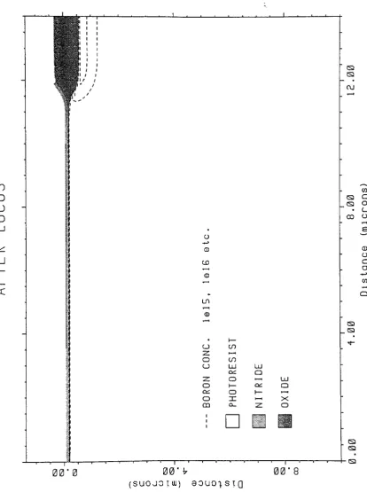
2.2).
After
the
field
oxidehas been
grown,
the
nitrideis
removed,
leaving
the
active areas accessible.One
ofthe
problems withthis
method ofisolation,
is
that
abirds beak
effectis
formed
due
to
a slightlifting
ofthe
nitridelayer
atthe
edge ofthefield
oxide.The
birds
beak
effectoftheLOCOS (Localized Oxidation
ofSilicon)
isolation
processis
aNitride-Protected
Active Area
Field Oxide
"^j^^
N-Well
7
P-Type Wafer
Figure
2.2:
Field Oxide Growth
Once
the
nitrideis
removed,
a sacrificial oxideis
grown, overthe
activeregions.
The
thickness
ofthis
oxideis
onthe
order of500
A.
The
entire waferis
implanted
with aboron,
device
threshold
adjustment,
implant.
This
threshold
adjustment
implant increases
the threshold
voltage ofboth
the
NMOS
andPMOS
devices,
thus
making
it
easierto
turn
onthe
PMOS
devices
and moredifficult
to turn
on
the
NMOS
devices.
The
sacrificial oxideis
then
removed andthe
gate oxideis
grown
to
athickness
of500
A.
Polysilicon
is
then
deposited
ontop
ofthe
gate oxide.Next
the
polysiliconis doped
using
aspin on glassdopant.
The
waferis heated
to
allowphosphorus
to
diffuse
into
the
polysilicon.The
glassis
then
etchedoff,
andthe
polysilicon
is
patterned,
using
the
fourth
masklevel.
The
unwanted polysiliconis
Polysilicon
Gate
Gate Oxide
Figure 2.3: Gate Oxide Growth
andPolysilicon Deposition
Next
the
wafers arepatterned,
using
the
fifth
masklevel,
andthe
wafers areimplanted
withboron
(BF2),
to
producethe
P+ source anddrain
areas ofthe
PMOS
devices. The
wafers arepatterned, using
masklevel
six, the
inverse
ofthe
fifth
masklevel.
The
wafers areagainimplanted,
but
this
time
withphosphorus, to
producethe
N+
source and
drain
areas ofthe
NMOS
devices
(see
figure
2.4).
Once
this
is
completed,
alow
temperature
oxide(LTO)
is
deposited using LPCVD
(Low
Pressure
Chemical Vapor Deposition).
This
oxideis
aninsulator between
the
metal andpolysilicon
layers.
The
wafers arethen
placedin
the
furnace
at900C for
30
minutesto
densify
the
deposited
oxide anddrive-in
and activatethe
source anddrain
areas ofthe
NMOS
andPMOS devices.
Boron (P
)
TTTT
^
7
Phosphorus
(Nf)
~n~
P+
Source/Drain
N*
Source/Drain
Figure 2.4:
N+/P+The
wafers arethen
patterned, using
masklevel
seven.The
contact cuts arethen
etchedthrough
the
LTO
using HF
for
an appropriate amount oftime,
depending
upon
the thickness
ofthe
oxideoverthe
sourceanddrain
regions andthe
etch rate ofthe
HF
bath.
Once
the
contacts areopened,
aluminumis
then
sputtered onthe
wafers,
afterwhichthe
aluminumis
patternedusing
mask#8,
and etchedin
aheated
aluminum etch
(figure
2.5).
Finally,
the
wafersaresintered,
that
is
putin
the
furnace
at
415C
with aforming
gas ambientto
improve
the
aluminumcontactsto
the
source,
drain,
andpolysilicon regions.Aluminum
wi!f
wnir
re
i
Figure
2.5:
Aluminum
Contacts
to
Source/Drain
Parameter
Extraction Techniques
Model
parametersareextractedby
applying
mathematical methodsto
variousmeasuredor simulated
device
characteristiccurves,
currentvs. voltage or capacitancevs. voltage.
The
required curve or curves aredefined
by
the
methodfor
extracting
aparticularparameter.
Two
examples of curves usedfor
model parameter extractionVd
family
ofcurves(drain
currentvs.drain
voltage,
for
givengatebias).
Additionally,
the
dimensions
ofthe
devices
may
be
varied andthe
parametermay
be
extractedfrom
a particular curve
based
uponthe
particularsizing
ofthe
device
andhow
that
curvediffers from
other curves producedfrom
different device
sizes.Examples
of suchdevice
sizesinclude large devices
(both
long
and widechannel),
short channeldevices,
and narrow channel
devices.
It
is
notnecessary
to
extract parametersexclusively from
measured curves.As
mentioned abovebriefly,
simulated curves canbe
usedfor
parameter extraction.The
big
advantage withthis
methodis
that
a particular processmay
be
simulatedusing
a simulationtool,
such asTSUPREM
4,
andthe
electrical performance ofthe
devices
simulated with adevice
simulationtool,
such asMEDICI.
With
these
tools
the
curvesnecessary
for
parameter extractionmay be
producedby
simulation,
andmodels
may
be
created withoutfabricating
realdevices in
silicon.Once
realdevices
have been
fabricated,
the
simulationsmay
be
calibrated sothat
the simulateddevice
models match
the
measureddevice
models accurately.This
process canbe
very
important
in reducing
the
time
it
takes
to
develop
aproductusing
a new process.A
simulated model can
be
providedto
circuitdesigners
long
before devices have been
produced
in
silicon andmodelsprovidedfrom
measureddevices.
IC-CAP
allowsthe
usertwo
methods of parameter extraction:direct
andparameter or set of parameters
directly
from
the
appropriate measured curve.Optimization
may
be
used afterdirect
parameterextraction,
andis
usedto
optimizethe
fit between
the
measured
curves andthe
simulated curves producedfrom
the
extracted model parameters.
The
fit is
optimizedby
varying
one or more modelparameters
from
their
extractedvalues andchecking
the
fit.
The
range over whichthe
parameters
may
be
variedis
setby
the
user,
as arethe
parametersbeing
optimized.Additionally,
the
orderin
which parametersareoptimized andpossibly
re-optimized,
and
the
numberof possible methods of optimizationis infinite.
Statistical
Parameter Extraction
Statistical
parameter extraction requires a"large"
amount of
data,
where30
or more samples constitutes alarge
samplesize,
and statistical proceduresfor
testing
the
data [4].
The
data
that
was usedfor
statistical parameter extraction wasthe
SPICE
model
decks for
the
measureddevices.
Each
measurementhas
acorresponding SPICE
model.
The Level 3 SPICE
models containthe
measured parametersfor
the
"large"device,
which meanthe
transistor
channelis
both
long
and wide(32^im
x32pm).
The
parameters extracted
include
VTO, U0, NSUB,
andTHETA
(the
zerobody
bias
threshold voltage,
surfacemobility,
substratedoping,
andthe
mobility
modulationfactor,
respectively).In
this experiment,
73
devices
weremeasuredperwafer,
with aOnce
the
SPICE
modelshave
been
collected,
the
individual
parameters areused
to
generatethe
average,
+3a,
and -3amodeldecks.
The
reasonthe
parameterswere used
is
that
it
was much easierto
collectthe
parameterdata
and performstatistics on
the
parametersthan
it
wasto
perform statistics on eachdata
point on allthe
I-V
curves.This
was alsopartially due
to
notfully
understanding
how
to
program
in
the
IC-CAP
macrolanguage.
The
standarddeviation for
the
sampledata
is
defined
as a measure ofthe
variability
withinthe
sample[4].
The
equationfor
sample standarddeviation
is
shown
in
eq.1.7
below [4].
s=
I
71-1frf-E5L
;=i
(1.7)
Using
Iman's
rule ofthumb,
that
99.7%
of all samples willbe
within3
standarddeviations
ofthe
samplemean, the
3
a
statisticalSPICE
models are chosen andcalculated
by
adding
andsubtracting
each model parameter's3a
valuefrom
the
parameter mean
[4].
The
nominal or average modelis
createdusing
the
parameteraverages.
Using
the
nominal modelfor
a given processto
simulate new circuitsbeing
designed for
that
particularprocess,
will give a goodindication
asto the
performance
of
the
circuit.Worst
case performancemay
be
examinedby
using
the
+3
a
and -3atreated
with caution.For
a particulardesign,
parametersmay
be
correlated with oneanother,
thus
a+3
a value of one parameter combined with a -3a
value of anotherparameter
may
be
the
true
worst case scenario and wouldhot
be
coveredby
simulation
using
the
average and3
a
models.Additionally,
a. good worst-casedesigned
circuit should operate wellbeyond
the
3
amodels,
and cases such asthe
one mentioned above should also
be
simulatedby
creating
a new statisticalmodel,
Procedure
Test
Chip
and
Device
Chip
Design
The
test
chip
usedfor
the
project was a modification ofthe
N-Well
CMOS
test
chip
designed
by
Bert
Berends in
August,
1993.
Robert Pearson
first
modifiedthe
layout
ofthe test chip,
by
moving
some ofthe
test
structures aroundfor better
grouping
of similartest
structures.Further
modifications werethen
madeby
moving
more of
the test
structures andredesigning
the
NMOS
andPMOS
transistors.
The
new
transistor
designs included
substrate and well contactsfor bulk
biasing
in
the
parameter extraction process.
Additionally,
the
three
transistor
sizes requiredfor
MOS
extractionusing IC-CAP
(large,
shortchannel,
and narrowchannel)
weredesigned
and placedin
a singleten
padconfiguration,
onefor
NMOS
and onefor
PMOS. This
wasdone because
the
switch matrix allowedthe
probe cardto
be
placedon
the
waferonce.The
connections couldthen
be
changedfor
eachtransistor
onthe
padsetwithout
lifting
up
the
probes.The device chip
contained a number of circuits madeup
of standard cellsrouted
to
output pads.The
standard cells rangedfrom
simpledevices,
such as aninverter,
NOR, NAND,
andXOR
cells, to
more complexcells,
such as a4-to-l
multiplexor cell and a
4-bit
ripple counter cell.Each
ofthe
cellswere routedto ten
padgroupings
for
use withthe
ten
pad probe card.The
standard cells werelaid
outapproximately
a4
Jim
scale and an8
(im scale ofdevices.
The
three
sizes werechosen
in
anattemptto
best
ensureworking devices
(even
if
only
atthe
largest
size),
and also
to
checkto
seeif fabrication
ofworking 2
(jmdevices
couldbe
performedwith
the
N-Well
CMOS
process atRIT's
Cleanroom
facilities.
The
purpose ofthe
device
chip
is
to
allowfor future
comparisons ofdevice
simulationsusing
the
statistical
SPICE
modelswithmeasuredoperation ofthe
devices.
An
example of oneof
the tests
whichmay
be
performedis
the
operation of aninverter.
The
simulatedandmeasuredvalues of
the
input
voltage,
at whichthe
inverter
output switchesfrom
low-to-
high
andhigh-to-low,
couldbe
compared.The
devices
chosenfor inclusion in
the
device
chip
weretaken
from
the
standard celllibrary
provided withthe
Mentor
Graphics3
v8.2_5 software
tools.
A
second metallayer
is
requiredfor
the
operation ofthe
device
chip,
andthe
processing
ofthis
second metallayer
wasleft for future
work.The
standardcellsusedin
the
device
chip
are aninverter,
a2-input
NAND,
anexclusive-OR,
a2-input
OR,
abuffer
withinverting
andnon-inverting
outputs,
aNAND
latch,
aD-flip flop,
a4-to-l
multiplexor,
a4-bit
ripplecounter,
aninput
padcell,
and an output padcell.The input
and output pads wereincluded
sothey
couldbe
tested
for
use withfuture
RIT,
N-Well
CMOS,
circuitdesigns.
CMOS
Processing
The
following
is
astep-by-step
description
ofthe
N-Well CMOS
processsteps.
STEP 1:
Twenty-five P-type
wafers wereobtained,
andthe
manufacturer'sdata
wasrecorded.One
ofthe
wafers was scannedfor
a particle count.The back
ofthe
wafers werescribed,
andthe
waferwasrescanned andthe
new particle countdata
wasrecorded.
The
wafers were scribedin
the
following
manner:15
device
wafers,
8
control
wafers,
and2
alignment wafers.The lot
number was also scribed onthe
wafers.
Selected
wafers werefour-point
probed andtheir
resistivity
was calculated.STEP 2: The
wafers werethen
cleanedin
anRCA
clean,
which consisted of aten
minuteAPM
bath,
afour
cyclerinse, two
minutesin
a50:1 HF
bath,
anotherfour
cycle
rinse,
aten
minuteHPM
bath,
rinsing
in
the
lower
and upper cascaderinser,
andfinally
placedin
the
SRD (Spin Rinse
Dry)
for
additionalrinsing
and spindrying.
Again
the
wafer measurefor
a particle countpreviously
was scanned andthe
newparticle count recorded.
STEP 3: The
wafers were placedin
furnace
tube
13
for
alignment oxidegrowth.
The
following
thermal
and chemical recipe was used:1000C for 10
minuteswith
6
slpmdry
02
and1
slpmN2,
1000C
for
55
minutes with2
slpmdry
02
and2
slpm wet
02,
1000C
for
5
minutes with7
slpm02
and1
slpmN2,
a15
minutetemperature
ramp up
to
1 150C
with7
slpm02
and1
slpmN2,
andfinally,
1150C
The
push ratewas12"
per
minute,
andthe
pull ratewas10"
per minute.
The
load
orderof
the
boat
was(from
load
endto
sourceend) CI
-C8,
Dl
-D15, Al,
andA2.
The
wafers wereinserted
withthe
top
of wafersfacing
toward
the
load
end ofthe
furnace.
After
the
wafers cooleddown,
the
oxidethickness
was measured on variouswafers.
STEP 4: The
wafers werethen
coated with resistusing
program3
onthe
WaferTrac.
This
program consists of a250C
prebakefor
120
seconds,
HMDS
prime and photo resist
coat,
and a45
second postbake at100C.
Next
the
alignmentwaferswere exposed on
the
stepper, using
masklevel
1,
the
N-Well
masklevel.
The
alignment wafers were
then
developed
using
program2
onthe
WaferTrac.
Program 2
consists of a
45
second prebake at115C,
the
developer cycle,
and a120
secondpostbakeat
120C.
The
alignment wafers werethen
examined under a microscopeto
determine
the
quality
ofthe
exposure anddevelop.
Once it
wasdetermined
that the
exposure and
develop
wasacceptable,
the
remaining
device
wafers were exposed anddeveloped.
The
control wafers were exposedseparately
from
the
device
wafers.Using
acontactaligner, the
control wafers wereexposedwiththe
top
half
ofthe
wafercovered
(the half
withthe
flat) by
a piece of sheet metal.The
wafers were etchedin
HF
untilthey
became
hydrophobic
(pulled
dry).
This
removedthe
oxidein
the
areaswhere
the
resisthad been
removed.STEP 5: Initial formation
ofthe
N-Wells
wasperformedwhenthe
wafers wereof energy.
Each
wafer wasimplanted
for
approximately
16
second,
with an arccurrent of
approximately
6
|iA.
STEP 6: The
waferswerethen
placedin
the
plasma asherfor 38
minutes,
andthe
resistwasremoved.
STEP 7: The
wafers wereRCA
cleaned asabove,
but
with a12
secondHF
dip.
STEP 8: The
wafers were placedin
furnace
tube
13,
for
N-Well drive-in
andoxide growth.
The
wafers were pushedin
at900C
at a rate of8" perminute,
withthe
sameboat
order asbefore,
and rampedup
to
1000C in 10
minutesin 4
slpmN2.
The
recipeis
asfollows:
1000C for
10
minutesin
8
slpmdry
02,
1000C for
26
minutes
in
6
slpm wet02,
1000C
for
20
minutesin 8
slpmdry 02,
15
minutetemperature
ramp up
to
1150C in 8
slpmdry
02,
1150C
for
1252
minutes(20 hrs.
52 min.)
in
4
slpmN2,
120
minuteramp down
to
800C
in
4
slpmN2,
and800C for
360
minutesin 4
slpmN2.
The
wafers were pulled at800C
at a rate of 8" perminute.
Oxide
thickness
measurements were performed onthe
control wafers onthe
well andnon-well
halves
ofthe
wafers.STEP 9: The
wafers werethen
etchedin
HF
untilthey
became
hydrophobic,
removing
any
oxide.After
the
HF
etch,
wafers wererinsed in
the
cascaderinses
andSTEP 10:
The
control wafers were thenfour-point
probed onboth
the
welland non-well
sides,
andresistivity
anddoping
levels
werecalculated.Control
wafersCI
andC2
were grooved and stained onthe
wellside,
and welljunction depth
measurements were made and recorded.
The
well/non-wellstep,
due
to the
oxidegrowthand removal was also measuredandrecorded.
STEP 1 1
:The
wafers wereplacedin furnace
tube
12
at950C for 40
minutesin
5.4
slpmdry 02,
to
grow a250
A
pad oxide.The
wafers were pushed and pulledat
850C
at arateof8"
per minute.
Temperature ramping
wasdone
in 4
slpm ofN2.
The
oxidethicknesses
weremeasured onthe
control wafersandrecorded.STEP 12: The
wafers werethen
putin
the
LPCVD
and a1000
A
target,
nitride
layer
wasdeposited
atatemperature
of800C.
The
boat
load
order wasCI
-C2,
Dl
-D15,
C3
-C4,
withthe
wafersfacing
toward the
sourceend ofthe tube.
The
deposition
time
was14
minutes.Nitride
thicknesses
were measuredand recorded.STEP 13:
Active
layer
lithography
was performed onthe
device
wafers, using
the
activelayer
mask,
mask2.
As
before,
testing
was performed onthe
alignmentwafers.
STEP 14: The
nitride was etchedin
the
RLE.
with a30
seemSF6
flow,
at150
Watts
and39.9
mTorr.An
etchtime
wasdetermined using
control wafersCI
-C4.
STEP 15:
P-Field
threshold
adjustmentlithography
wasperformed
next.The
coated on
top
ofthe
previouslayer.
Due
to
this,
the
250C
prebakestep
wasremoved
from
the
resistcoating program,
andreplaced with afive
seconddelay.
The
control wafers wereexposedon
the
contactaligner withthe
bottom
side covered(flat
side exposed).
STEP 16: The
wafers werethen
implanted
with aboron P-field
threshold
adjustment
implant
to
preventtransistor turn
onin
the
field
regions.Wafers Dl
-D7
were
implanted
with a2E13
ions/cm2dose
ofBn
at33
KeV,
whileD8
-D15
were
implanted
witha4E13
ions/cm2dose
ofBu
at33
KeV.
STEP 17: The 21
wafers were plasma ashedfor 40
minutes andthe
resist wasremoved.
STEP 18: The
wafers werethen
cleanedin
the
standardRCA
cleanprocess,
and spin
dried.
STEP 19: The
wafers were placedin
tube
13
for field
oxide growth.The
following
thermal
recipe was used:800C
in
5.5
slpmN2
and5.5
seemdry
02
for
15
minutes,
ramp
to
1 100C
for
20
minutes,
25
minutes at1
100,
ramp
down
to
950C
for
30
minutes,
15
minutes at950C,
300
minutesin
5
slpm wet02
at950C,
30
minutes
in 5
slpmN2
at950C,
ramp down
to
800C
in
5
slpmN2
for
30
minutes.A
calibrated mass
flow
controller(MFC)
was usedto
achievethe
5.5
seem02
flow.
During
the
last
minutebefore
the
5
slpm wet02
growthcycle,
the
02
flow
wasturned
and
turned
back
on.The
push-pull rate was 8" per minute.The
measuredfield
oxidethicknesses
were around7000
A,
slightly less
than the
target thickness
of7500
A.
STEP 20:
The
oxinitride was etchedby dipping
the
wafersin
HF
for
3
minutes, 50
seconds.They
werethen
rinsed
and spundry.
STEP
21:
The remaining
nitride wasetchedin
the
RLE.
for
75
seconds,
at150
watts,
30
seemSF6,
and a pressureof40
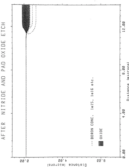
mTorr.STEP 22: The
padoxideunderthe
nitride was etchedfor 35
to
45
secondsin
buffered
HF
untilthe
areasbetween
the
chipspulleddry.
STEP
23: A
standardRCA
clean was performed with out theHF
dip.
The
waferswere
then
rinsed
anddried in
the
SRD.
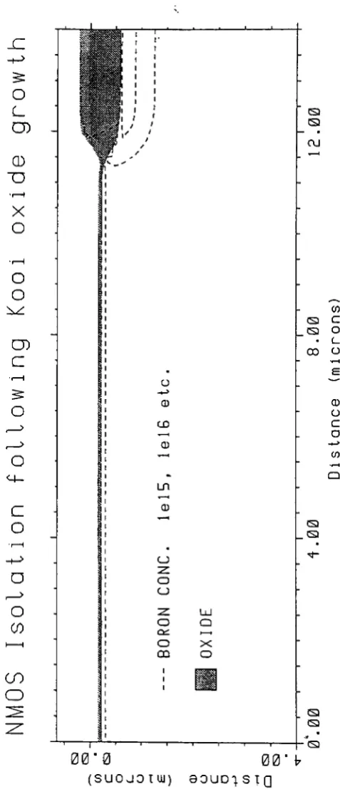
STEP 24: A
sacrificial oxide was grownin
furnace
13,
withthe
following
thermal
recipe: pushin
at900C
ata rate of 8"per
minute,
4
slpmN2
for 25 minutes,
2
slpmdry
02
and4
slpm wet02
for
25
minutes,
35
minutesin
5
slpmdry
02,
pullat 8"
per minute.
The
target thickness
was600
A
to
700
A,
but
the
measuredthicknesses
were818
A
to
967
A.
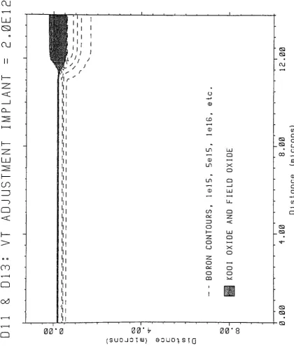
STEP 25:
The devices
wereimplanted
withboron
(Bu)
for device
threshold
adjustment.
The
wafers wereimplanted
with a range ofdoses,
additionally D4
andD12
wereimplanted
with a punchthrough
preventionimplant
of2.5E11
ions/cm2 atD1&D9
1E12
ions/cm2,
D2&D10
1.5E 12
ions/cm2,
D3-D5&D11-D13
2E 12
ions/cm2,
D6&D14
2.5E12
ions/cm2,
D7&D15
3E12
ions/cm2,
D8
noimplant.
STEP 26: The
sacrificial ox