EFFECT TYPE OF CONDUCTIVE INK TO STRETCHABLE PRINTED CIRCUIT UNDER THERMAL PERFORMANCE
NURUL SYAFIKA BT ROZALI
A report submitted
in fulfilment of the requirement for the degree of Bachelor of Mechanical Engineering (with Honours)
Faculty of Mechanical Engineering
UNIVERSITI TEKNIKAL MALAYSIA MELAKA
DECLARATION
I declare that the project entitled “Effect Type of Conductive Ink to Stretchable Printed
Circuit under Thermal Performance” is the result of my own work except as cited in the
references.
Signature : ...
Name : Nurul Syafika Binti Rozali
APPROVAL
I hereby declare that I have read this project report and in my opinion, this report is
sufficient in terms of scope and quality for the award of the degree of Bachelor of
Mechanical Engineering.
Signature : ...
Supervisor’s Name : ...
DEDICATION
i ABSTRACT
ii ABSTRAK
iii
ACKNOWLEDGEMENTS
Firstly, I would like thank to Allah Almighty for gave me strength and blessing that
allowed me to complete this research within the time given. Next, I would like to take this
chance to express the deepest appreciation to my supervisor, Dr. Mohd Zaid Bin Akop,
who was continuously give advice, support and spending his valuable time and energy to
make this research complete successfully. It is a great honour to work under his
supervision. I am very thankful for having such a good adviser like you.
I would like to express my sincere gratitude to my family members for their
encouragement and always support me in doing this research. Very special thanks to my
group members, Nurul Hasanah Binti Sobri, Muhammad Aiman Bin Suhaimi, Muhammad
Zaim Bin Azmi, Abdul Mueezz Bin Abdul Raheem and Muhammad Amin Bin Othman for
their invaluable help and kind endless help.
Lastly, I humbly extend my thanks to Siti Ashikin Binti Azli, master degree student who
iv
TABLE OF CONTENTS
PAGE DECLARATION
DEDICATION
ABSTRACT i
ABSTRAK ii
ACKNOWLEDGEMENTS iii
TABLE OF CONTENTS iv
LIST OF TABLES vi
LIST OF FIGURES vii
LIST OF APPENDICES x
LIST OF ABBREVIATIONS xi
LIST OF SYMBOLS xii
CHAPTER
1. INTRODUCTION 1
1.1 Background 1
1.2 Problem Statement 3
1.3 Research Objectives 5
1.4 Scope of Project 5
1.5 Planning and Execution 6
2. LITERATURE REVIEW 8
2.1 Introduction 8
2.2 Conductive Ink 8
2.3 Filler 11
2.3.1 Carbon Black 12
2.3.2 Nanoparticles 14
2.3.2.1 Singlewalled Carbon Nanotubes 17
2.3.3 Weight Percentage of Filler Loading 19
2.4 Substrate 21
2.4.1 Thermoplastic Polyurethanes 24
2.4.1.1 Thermoplastic Polyurethanes Properties 26
2.5 Four-Point Probe System 29
3. RESEARCH METHODOLOGY 31
3.1 Overview of Research 31
3.2 Materials 34
3.2.1 Carbon Black 34
3.2.2 Single Walled Carbon Nanotubes 35
3.3 Sample Preparation 36
3.4 Experimental 40
3.4.1 SEM Analysis 40
3.4.2 Sheet Resistance under Room Temperature 41 3.4.3 Sheet Resistance under Designed Temperature 42
v
4. RESULT AND DISCUSSION 48
4.1 Introduction 48
4.2 SEM Analysis for Carbon Black and Singlewalled Carbon Nanotubes 49
4.2.1 Carbon Black SEM’s Analysis 49
4.2.2 Singlewalled Carbon Nanotube’s SEM Analysis 51 4.3 Case I: Sheet Resistance under Room Temperature 53 4.4 Case II: Sheet Resistance under Designed Temperature 54
4.5 Case III: Sheet Resistance under Strain 59
5. CONCLUSION AND RECOMMENDATIONS 66
5.1 Conclusion 66
5.2 Recommendations 68
REFERENCES 70
vi
LIST OF TABLES
TABLE TITLE PAGE
2.1 Thermal conductivity of conductive filler 12
2.2 TPUs components 25
3.1 Typical properties of CB bare conductive inks 35
3.2 Typical properties of SWCNTs 36
3.3 Screen frame dimensions 37
4.1 Elemental composition for CB 50
4.2 Elemental composition for SWCNTs 52
5.1 Summary for average weight of percentage filler loading for both
inks
67
5.2 Summary of total percent increment of Rs after applied strain for
both inks
67
vii
LIST OF FIGURES
FIGURE TITLE PAGE
1.1 Gantt chart for PSM I activities 6
1.2 Gantt chart of activity details and their respected time frame for
PSM II
7
2.1 Components of conductive ink 9
2.2 Illustration of conductive filler after heat applied 13
2.3 Illustration of CNTs atomic structure 15
2.4 Atomic arrangement of singlewalled and multiwalled CNTs 16
2.5 Simulation of SWCNTs buckling 18
2.6 Sheet resistance versus contents of active phase for several volume
fraction of CB fillers at different curing time
20
2.7 Thermal conductivity versus weight percentage of CNTs for well
and poorly dispersed
21
2.8 Solid substrates, flexible substrates and stretchable substrates 22
2.9 A hybrid circuit consisting of rigid island and stretchable
interconnect
23
2.10 TPUs structure composes of Soft Segments (SS), Hard Segments
(HD) and Hydrogen Bond
viii
2.11 Basic chemistry of TPUs 27
2.12 The relationships shore A to shore B 28
2.13 Schematic diagram of four-point probe configuration 29
2.14 Four-Point Probe Systems 30
3.1 Flow chart of the methodology 33
3.2 Carbon black bare conductive ink 34
3.3 Top view of screen frame printing 37
3.4 The illustration of the screen printing process from side view 38
3.5 The illustration of the screen printing process from side view 38
3.6 The illustration of the screen printing process from top view 39
3.7 Oven used for curing process of SWCNTs 39
3.8 Top view of marked sample 40
3.9 Scanning Electron Microscope 41
3.10 Sheet resistance measured at room temperature 42
3.11 Illustration for measuring sheet resistance technique 42
3.12 Front view of experiment set up for sheet resistance at designed
temperature
43
3.13 Top view of experiment set up for sheet resistance at designed
temperature
44
3.14 Thermal imaging analyzer used 44
3.15 Image captured by thermal imaging analyzer for temperature 100°C 44
3.16 Top view of experiment set up for sheet resistance under strain 45
3.17 Top view of clipped sample at the vernier calliper 46
3.18 Carbon black stretched samples 46
ix
4.1 SEM micrograph and element analysis for carbon black surface
(a) Spectrum 1 (b) Spectrum 2
49
4.2 SEM micrograph and element analysis for SWCNTs surface
(a) Spectrum 1 (b) Spectrum 2
51
4.3 Bar chart for Rs of CB and SWCNTs at room temperature 54
4.4 Bar chart for sheet resistance of CB versus designed temperature 55
4.5 Bar chart for sheet resistance of SWCNTs versus designed
temperature
56
4.6 Graph of sheet resistance in percent reduction for CB ink after heat
applied versus design temperature
57
4.7 Graph of sheet resistance in percent reduction for SWCNTs ink after
heat applied versus design temperature
58
4.8 Graph of sheet resistance for CB versus strain 60
4.9 Graph of sheet resistance for SWCNTs versus strain 61
4.10 Graph of percent increment of average sheet resistance after strain
applied at room temperature
62
4.11 Images of stretched CB samples 63
x
LIST OF APPENDICES
APPENDIX TITLE PAGE
A ASTM F390 standard test method for sheet resistance 75
C1 Data sheet for carbon black bare conductive ink 79
xi
LIST OF ABBREVATIONS
SPC Stretchable Printed Circuit
PCB Printed Circuit Board
SWCNTs Singlewalled Carbon Nanotubes
MWCNTs Multiwalled Carbon Nanotubes
CB Carbon Black
TPUs Thermoplastic Polyurethanes
PDMS Polydimethylsiloxane
RT Room Temperature
SEM Scanning Electron Microscopy
CNTs Carbon Nanotubes
TPEs Thermoplastic Elastomers
SS Soft Segments
HD Hard Segments
T Temperature
xii
LIST OF SYMBOLS
wt.% - Weight percentage
Ag - Silver
Mg - Magnesium
Si - Silica
Rs - Sheet resistance
I - Current
1 CHAPTER 1
INTRODUCTION
1.1 Background
The 1950s was a decade of the stretchable circuit was introduced in a very limited
and slight way. It is also can be known as stretchable printed circuit (SPC). The simplest
definition for stretchable printed circuit is a pattern of conductive traces bonded on
stretchable substrates and in other words, it is a perfect solution for electronics packaging
needs. Due to its capabilities and reliability, stretchable printed circuit has a valuable
position compared to traditional printed circuit in worldwide printed circuits market.
Stretchable printed circuit are being used widely in everyday technology and electronics in
addition to high-end, complex completed components. The usage of SPC in modern
portable electronics, hard disk and desktop printers are a few of the most outstanding
examples.
Nowadays, stretchable printed circuit is mainly used in small or thin electronic
institution compared to traditional printed circuit board. It is due to several good features
of stretchable printed circuit compared to traditional printed circuit board (PCB). The first
one is, SPC is highly stretchable and foldable compared to traditional PCB that is rigid.
Next, stretchable printed circuit can be folding without affecting the signal transfer
function. Application of the product also will be reduce, significantly reduce weight,
2
added flexibility and lighter weights allow the printed circuit to absorb and reduce the
impact of the vibration to itself as well as any solder joints in connections. Stretchable
printed circuit also can be use in harsh environment because it is built with materials that
are have the waterproof, moisture proof, shock proof, high temperature oil and corrosion
resistance properties.
In general, stretchable printed circuit comprising of filler, binder, solvent and
substrate. There are a lot of different type of conductive filler that has being use in
industry for example singlewalled carbon nanotubes (SWCNTs), multiwalled carbon
nanotubes (MWCNTs), carbon black (CB), silver and graphene. Solvent also one of the
important substances in the stretchable printed circuit that will increase the cross-linking of
polymer. Cross-link is bond that links one polymer chain to another. Next, it is also a
variety of material for improved thermal physical and chemical properties. Binder is a
polymer, which for particle redistribution and restoration of conductivity upon solvent
evaporation for example epoxy and resin. There are a few types of flexible substrate that
has been used for example Thermoplastic Polyurethanes (TPUs) and Polydimethylsiloxane
(PDMS).
Conductive inks are a mixture of conductive particles or filler, polymer binders,
and dispersing solvents. The combination of the three elements will form conductive ink,
which conducts electricity. They have been used in many electronics in industry for
example in metallization of microcircuits, solar cells, large area electronic structures, and
solder for microelectronics packages. Other than that, it is also technologies that
compatible with many substrate surfaces including polyester, glass, and ceramics, and can
3
This research will focus on the different types of conductive inks in stretchable
printed circuit. Different conductive inks will have different properties. In other words,
they will have the different in mechanical, thermal and physical properties that will affect
the electrical conductivity of the conductive ink. The goal of this study is to investigate the
effect thermal and strain on sheet resistance of different type’s conductive ink.
In electronic industry, good conductivity of polymer-based conductive ink plays a
big role that related to cost effective. Thermal conductivity that can be defines as a
property of a material's ability to conduct heat while thermal resistance is a measure of a
material's ability to prevent heat from flowing through it. In the other words, the greater
conductivity, the lower its resistance.
1.2 Problem Statement
Over the past few years, in order to improve and upgrade the industry technologies,
printed circuit board is invented from rigid printed circuit board to stretchable printed
circuit board. This is due to the limitation of the usage rigid printed circuit in industry for
example it has fixed mode or shape depending on the shape of the product, rigid and has no
anti-vibration. The fixed board is replaced by flexible substrate since it has flexible and
stretchable properties. Conductive inks that are both stretchable and flexible are
performing as better application in stretchable printed circuit electronic devices. Therefore,
the demand of highly flexible and bendable of printed circuit is grow rapidly. To have high
quality of stretchable conductive ink, it must be able to expose with high level of
temperature, capable on has good adhesive strength with the substrate while maintaining
the electrical conductive performance. However, the current stretchable conductive ink
4
with arbitrary shapes like for example surface texture of human skin. It is significant to do
the further study on the effect of mechanical test to the electrical performance of the
conductive ink while making it is suitable to be applied in high performance application. In
this study, the mechanical test includes of strain for several elongation.
Next, the electrical performances, which are the conductivity of the stretchable
conductive ink, also have certain limitation under the thermal application. As mention
before, in order to improve the standard of the stretchable conductive ink, it must be able to
be implemented at high temperature conditions. Therefore, it is very important to
investigate the particle’s behavior of the conductive ink and compatibility between inks
with the substrate since the physical properties of the substrate might affect the
performance of the stretchable conductive ink. The conductive ink that has been used in
this study are singlewalled carbon nanotubes and carbon black, which has their own
properties.
These problems will be study based on several parameters for example the effect of
temperature and strain towards the resistivity of the conductive inks. Therefore, this
research will cover on the effect of different type of conductive ink to stretchable printed
circuit under thermal performance. CB and SWCNTs has been used to improve and
enhance a better quality of stretchable printed circuit. Next, the aim of this study is to
conduct experiment by using SWCNTs and CB that have a better conductivity and high
5 1.3 Research Objective
The objectives for pursuing the current research topic are:
1. To determine the effect of temperature to sheet resistance of CB and SWCNTs for
enhance the material properties.
2. To study the effects of strains to the sheet resistance of CB and SWCNTs at room
temperature for upgrade the functionality.
3. To study the effects weight percentage of filler loading in the conductive inks to the
sheet resistance for improve the electrical performances.
1.4 Scope of Project
The scopes of this project are listed as below:
1. Screen printing of conductive ink on TPUs substrate.
2. Measure sheet resistance of conductive ink using four-point probe:
Elevated temperature at 32 °C (RT), 40 °C, 60 °C and 100 °C
Strain at 20 %, 40 %, 60 % and 80 % of elongation
6 1.5 Planning and Execution
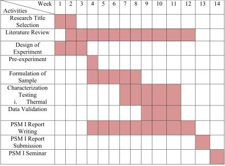
The details of research activities for PSM I are shown as in Figure 1.1 below.
Figure below illustrates the research activities for PSM 1 that includes the process of
research title selection, literature review, designing the experiment, pre-experiment,
formulation of samples, material characterization testing for thermal analysis, data
validation, report writing and followed by report submission and lastly PSM I Seminar.
The material characterization includes mechanical and thermal testing.
Week
Activities 1 2 3 4 5 6 7 8 9 10 11 12 13 14 Research Title
Selection
Literature Review Design of
Experiment Pre-experiment
Formulation of Sample Characterization
Testing i. Thermal Data Validation
PSM I Report Writing PSM I Report
[image:22.595.84.526.322.648.2]Submission PSM I Seminar
7
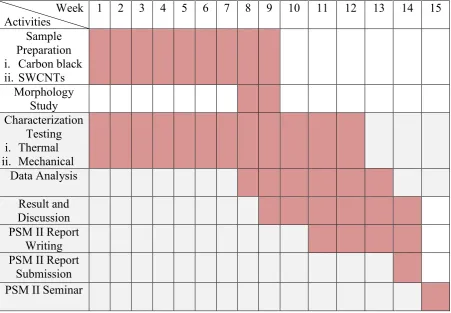
For PSM II, the research activities started with the sample preparation for both
conductive inks, which are CB and SWCNTs. Next, the activity is followed by the surface
morphology study by using Scanning Electron Microscopy (SEM) analysis,
characterization testing under thermal and mechanical test. SEM analysis was study to
analyze the particles content in the both conductive inks. The thermal test includes of
supplying elevated temperature to the samples starting with 40 °C, 60 °C and 100 °C. For
the mechanical test, it is includes of applying strain at 20%, 40%, 60% and 80% of
elongation to the samples. After all the testing completed, proceed with the data analysis,
result and discussion. The research activities for PSM II stage are detailed out as in Figure
1.2 below.
Week
Activities 1 2 3 4 5 6 7 8 9 10 11 12 13 14 15 Sample
Preparation i. Carbon black ii. SWCNTs Morphology Study Characterization Testing i. Thermal ii. Mechanical Data Analysis Result and Discussion PSM II Report
Writing PSM II Report
[image:23.595.81.533.394.707.2]Submission PSM II Seminar
8 CHAPTER 2
LITERATURE REVIEW
2.1 Introduction
In this chapter, a review on conductive ink, filler, substrate, four-point probe
system and the properties of the conductive ink including thermal, electrical and physical
properties have been discussed further.
2.2 Conductive Ink
Conductive ink plays a big role in stretchable printed circuit. The definition of
conductive in electrical view is the ability of the material or substances to conduct
electricity. With high conductivity of the material, such as metal, the electric current will
able to flow easily when voltage is exerted. It is also simply stated by D. Banfield (2000),
material with lower resistance will conduct electricity more efficiently compared to
material that has high resistance. Electrical resistivity or in other words, specific electrical
resistance is a parameter to measure how potentially conductors to resist the flow of
electric current. Next, the conductivity is inversely proportional to the resistivity, which is
high conductivity of conductor or material will results a lower resistivity.
Nowadays, the market and manufacture conductive ink showing sign of growth due