Rochester Institute of Technology
RIT Scholar Works
Theses Thesis/Dissertation Collections
5-2015
Design and Analysis of High Frequency Power
Converters for Envelope Tracking Applications
Trevor Chase Smith
Follow this and additional works at:http://scholarworks.rit.edu/theses
This Thesis is brought to you for free and open access by the Thesis/Dissertation Collections at RIT Scholar Works. It has been accepted for inclusion in Theses by an authorized administrator of RIT Scholar Works. For more information, please [email protected].
Recommended Citation
Design and Analysis of High Frequency
Power Converters for Envelope Tracking Applications
By
Trevor Chase Smith
A Thesis Submitted in
Partial Fulfillment of the
Requirements for the Degree of MASTER OF SCIENCE
in
Electrical Engineering
Approved by:
PROF__________________________________________________________ (Dr. Sergey E. Lyshevski, Thesis Advisor)
PROF______________________________________________________________ (Dr. James E. Moon, Thesis Committee Member)
PROF______________________________________________________________ (Dr. Edward E. Brown, Thesis Committee Member)
PROF__________________________________________________________ (Dr. Sohail A. Dianat, Department Head)
DEPARTMENT OF ELECTRICAL AND MICROELECTRONIC ENGINEERING
KATE GLEASON COLLEGE OF ENGINEERING
ROCHESTER INSTITUTE OF TECHNOLOGY
Acknowledgements
Abstract
Contents
Chapter 1: Introduction ... 1
1.1. High Frequency Power Electronics ... 1
1.2. Thesis Organization ... 3
Chapter 2: Conventional DC/DC Converters ... 4
2.1. Switching Loss in a Traditional Switch-Mode Converter ... 4
2.1.1 Turn-on Losses in the High-side Switch ... 5
2.1.2 Turn-Off Losses in the High-side Switch ... 11
2.1.3 Low-side Switch Losses ... 13
2.2. Diode Reverse Recovery Effect ...14
2.3. Control Law Design ...17
Chapter 3: ZVS and ZCS Converters ... 23
3.1. Introduction ...23
3.2. Resonant Gate Driving Techniques...26
3.3. High Side Gate Driving ...30
3.4. Proposed Digital Zero Voltage Switching Controller ...36
3.4.1 Envelope Detection of an Amplitude Modulation RF Signal ... 37
3.4.2 Bandwidth Reduction ... 39
Chapter 4: Experimental Results and Simulations ... 42
4.1. Introduction ...42
4.2. Closed Loop Simulations ...42
4.2.1 Method for Sensing Inductor Current ... 45
4.3. Simulation and Modeling of Half-Bridge Gate Drivers ...45
4.5. Simulation and Modeling of a Zero Voltage Switching Boost
Converter ...57
4.6. Experimental Results for a ZVS Boost Converter ...59
4.6.1 Closed Loop System and Frequency Response ... 62
4.7. Conclusion ...68
4.7.1 Summary ... 68
4.7.2 Proposal for Future Work ... 70
List of Figures
1.1: Traditional RF PA Loss and Envelope Tracking Loss ... 2
2.1: Turn-On Switching Waveforms Observed in SMPS ... 5
2.2: Turn-Off Switching Waveforms Observed in SMPS ... 11
2.3: Diode Reverse Recovery Voltage and Current Waveforms ... 16
2.4: Voltage Mode Control Scheme ... 18
2.5: Current Mode Control Scheme ... 20
2.6: Voltage Mode Feedback Error Control Loop ... 21
3.1: Switching Waveforms Observed in Traditional Hard-Switching (a), and Soft-Switching ZVS Applications (b) During Switch Turn-on. ... 24
3.2: ZVS Boost Switching Waveforms ... 25
3.3: Conventional Gate Driving Scheme for Synchronous Step-down Converters ... 26
3.4: Resonant Gate Driving Scheme for Synchronous Step-down Converters ... 27
3.5: High Side Bootstrap Circuit in a Boost Converter Application ... 31
3.6: Transformer Coupled Gate Drive in a Boost Converter Application ... 32
3.7: SPICE Schematic for Transformer Coupled Gate Driving ... 35
3.8: SPICE Simulation for Transformer Coupled Gate Drive... 36
3.9: Block Diagram of Proposed Digital ZVS Two-Phase Converter ... 37
3.10: Envelope Detection Proximity for Envelope Tracking Modulation ... 39
3.11: AM RF Signal Generation and Envelope Detection Simulink Model ... 40
3.12: Output Scope Envelope Waveform and Original Single-Tone AM Signal ... 41
4.1: Boost Converter Simulink Schematic ... 43
4.2: Start-up Transient Response of Type II and III Compensators ... 44
4.3: Load Step Transient Response of Type II and III Compensators ... 44
4.4: Technique for Sensing Inductor Current. ... 45
4.5: PSPICE Schematic for GaN and MOSFET Devices ... 47
4.6: Measuring Gate Charge Waveforms with Vendor Models ... 47
4.7: PSPICE Gate Charge Simulation for CSD18537N MOSFET 40V at 2A ... 48
4.8: PSPICE Gate Charge Simulation for EPC2020 GaN FET 40V at 2A ... 48
4.10: EPC9033 60 V Half-Bridge GaN Module. ... 50
4.11: Test Circuit for Capturing Gate Charge Waveforms ... 50
4.12: Experimental Gate Charge Waveforms: (a) GaN EPC2020; (b) MOSFET CSD18537N ... 51
4.13: Test Setup for Efficiency Evaluation ... 51
4.14: GaN and MOSFET Efficiencies at 24 W Output Power for Various Switching Frequencies ... 52
4.15: 24 W Half-Bridge GaN Step-down Converter at (a) 2 MHz and (b) 300 KHz. .. 53
4.16: TI NexFET™ Power Block Technology Dual MOSFET Package ... 54
4.17: TI NexFET™ Power Block™ Evaluation Platform TPS53819 ... 54
4.18: 300 KHz Efficiency Surface Plots of EPC9033 vs. CSD87350 ... 56
4.19: 900 KHz Efficiency Surface Plots of EPC9033 vs. CSD87350 ... 57
4.20: PSPICE Schematic for ZVS 2-Phase Boost Converter ... 58
4.21: PSPICE Simulation of ZVS Boost Converter. ... 59
4.22: 30W Multiphase ZVS Boost Converter Prototype and Layout Design ... 60
4.23: ZVS Boost Converter Switching Waveforms at 1 MHz ... 61
4.24: ZVS Boost Converter Switching Waveforms at 3 MHz ... 61
4.25: Efficiency Curves Comparing ZVS vs. Hard-switched Boost Converter. ... 62
4.26: Optimized Transient Response for Digital Step-Down Converter Operating at 500 KHz with 3A Output Loaded (a), and, Unloaded (b), under Type III Compensation. ... 63
4.27: Optimized Transient Response for Digital Step-Down Converter Operating at 1MHz with 3A Output Loaded (a), and, Unloaded (b), Under Type III Compensation. ... 64
4.28: Pole Zero Placement Coefficients for 500KHz Frequency Response ... 65
4.29: Pole Zero Placement Coefficients for 1MHz Frequency Response ... 65
4.30: Magnitude and Phase Frequency Response Plots for 500 KHz Operation ... 66
List of Tables
4.1: EPC GaN Devices for Evaluation ... 46
4.2: State-of-the-Art MOSFET Devices for Evaluation ... 46
4.3: Input/Output Boost Converter Specifications ... 59
Glossary of Terms
AC Alternating Current
AM Amplitude Modulation
BJT Bipolar Junction Transistor
CAD Computer Aided Design
CCM Continuous Conduction Mode
CMC Current Mode Control
DC Direct Current
DSP Digital Signal Processing
DR Diode Rectification
DCM Discontinuous Conduction Mode
EMC Electro Magnetic Compatibility
EMI Electro Magnetic Interference
FM Frequency Modulation
GaN Gallium Nitride
IC Integrated Circuit
LGA Land Grid Array
MHz Mega Hertz
MIF Maximum Impedance Frequency
MOSFET Metal Oxide Semiconductor Field Effect
Transistor
MRC Multi-Resonant Converter
PA Power Amplifier
PCB Printed Circuit Board
PID Proportional Integral Derivative
PRC Parallel Resonant Converter
PWM Pulse Width Modulation
PSM Pulse Skip Modulation
RF Radio Frequency
RMS Root Mean Square
SEPIC Single Ended Primary Inductor Converter
Si Silicon
SiC Silicon Carbide
SMPS Switch-Mode Power Supply
VHF Very High Frequency
Chapter 1:
Introduction
1.1.
High-Frequency Power Electronics
There are various electronic systems which can benefit from higher speed power designs. One in particular is in the communications industry: RF power amplification. Most RF communication systems use power amplifiers (PA) to convert low-power signals into larger power RF signals for driving the antenna of a specific transmitter. The majority of PA designs utilize switch-mode pulse-width-modulating (PWM) converters as the power source to operate RF amplifiers. Typically, the converter is set to a fixed peak power level, and consequently, waveforms with non-constant envelopes incur an increase in power dissipation during the valley regions of the modulation cycle. This process causes significant efficiency degradation for the overall system.
Traditional Power Loss
Time (us/ns) Amplitude
Envelope Tracking Power Loss
Time (us/ns) Amplitude
Figure 1.1: Traditional RF PA Loss and Envelope Tracking Loss
To achieve successful envelope tracking, the power supply must be capable of switching at frequencies greater than 5 MHz, as most modern RF waveforms observe a bandwidth of ~1 to 5 MHz. This poses a troublesome problem for power engineers because at these frequencies, the switching loss of conventional “hard-switching” MOSFETs can be quite substantial. This has led designers to pursue “soft-switching” methods to compensate for the efficiency loss at high PWM frequencies. It has also lead to the popularity and industrial development of gallium nitride (GaN) power transistor technologies. TheseGaN based devices are known to have higher efficiencies, work at higher frequencies, and offer higher power densities as compared to silicon metal-oxide-semiconductor technology.
stored energy during each switching cycle, resulting in power loss. These losses are generally proportional to the PWM switching frequency of the design. To gain a more comprehensive understanding of the switching loss attained in a PWM converter, the actual design topology should be analyzed, as the mechanism for switching loss can vary by converter topology.
1.2.
Thesis Organization
Chapter 2:
Conventional DC/DC Converters
2.1.
Switching Loss in a Traditional Switch-Mode
Converter
For the switching loss analysis, the power loss in typical synchronous “step-up” and “step-down” power stages will be evaluated. These types of topologies consist of high-side and low-side switches that operate in a complementary fashion. When one device is off, the other device is on, and vice versa. The power stage and the associated drive circuitry are often referred to as being in a half-bridge configuration. For either topology, the devices must be prevented from turning on simultaneously. Therefore, a small amount of dead-time is necessary in most practical designs. Dead-time is the length of time that both switches are kept off during a switching cycle.
2.1.1 Turn-on Losses in the High-side Switch
The high side switch is the main power stage in a synchronous step-down converter. The synchronous term is used to describe a technique of replacing a diode stage with an active switching element. In a step-up converter, the high side switch operates as a synchronous rectifier. For both topologies, power losses can be attributed to conduction, switching, and gate charging.
Conduction loss can be described as
2 dson out out Cond
in
R I V
P
V
, (1)
where Rdson is the on-state conduction resistance; Iout is the RMS drain
current; Vin is the input voltage; Voutis the output voltage.
The high side switching losses can be analyzed by observing the drain-source voltage and current waveforms during the turn-on and turn-off transitions. Figure 2.1 describes the switching loss waveforms for a traditional “hard-switched” design.
VDS
ID
Traditional Turn-ON Switching Loss
VGS
VGS
t1 t2 t3
In general, the turn-on power loss can be described as
( )
2
sL sH in sw out
Switchloss
t t V F I
P , (2)
where Vinis the input voltage; Fswis the PWM switching frequency; tsLis the
low to high transition time; tsHis the high to low transition time; Ioutis the
RMS drain current.
The high-low and low-high transition times are dictated by the device’s gate charge and driver currents defined as
C sH
GDH
Q t
I
and C sL
GDL
Q t
I
, (3)
where QCis the total gate charge needed to bring the gate-source voltage
through the Miller turn-on region as discussed in Section 2.1.1.2; tsHis the
high-to-low transition time; tsLis the low-to-high transition time; IGDis the
gate drive current. The total gate charge is normally specified by the manufacturer’s datasheet. But the associated driver current must be calculated or measured.
The high side driver gate current, which is the result of the device gate-charge during turn-on and the average high-low transition time, is
G P
GDH
DRV
V V
I
R
where VGis the gate drive voltage; VPis the switch plateau voltage; andRDRVis
the series driving resistance.
The power lost in the gate drive circuit is approximated as a function of the total gate charge of each device being driven, as well as the speed of the gate-drive switching frequency. Assuming that the high-side and low-side switches are chosen to be identical, the total gate drive loss is found as
2
gate sw HS LS DR sw C DR
P F Q Q V F Q V . (5)
The gate drive voltage is typically from 5 V to 12 V depending on the MOSFET technology. New designs utilize logic-level devices in order to improve efficiency.
2.1.1.1 Loss Due to Common Source Inductance
When power is first applied, the CSI reacts to an initial di/dt event that reduces the effective gate-source voltage. This voltage, due to CSI, may be represented as
2p p out
SL CS CS
sH
I I di
V L L
dt t
. (6)
The driver gate current, which is the result of the device gate-charge during turn-on and the average high-low transition time, is calculated as
G SL P
GDH
DRV
V V V
I
R
. (7)
We substitute in the appropriate equation for the CSI, and the gate drive current becomes
2
p p out
G CS P
sH
GDH
DRV I I
V L V
t I R
. (8)
From equation (3) we know the specified high-low transition time takes into account the gate current, so we combine like terms and rearrange to yield 2 Q p p out GDH CS GS G P GDH DRV DRV I I I L V V I R R
The only difference here is that instead of using the total gate charge, we must use the high-side gate-source charge. Rearranging (9) and solving for IGDH, one finds the final gate drive current as
2 G P GDH p p out DRV CS GS V V I I I R L Q
. (10)
Once the gate driver current is known, the associated switching power loss incurred during the time between device turn-on and the Miller Plateau is
2
2
p p
in GS sw out
Switchloss
GDH I
V Q F I
P I
. (11)
The switching loss is proportional to the gate charge of the MOSFET as well as the switching frequency of the application.
2.1.1.2 The Miller Gate Charge Effect
This increases the equivalent charge required during each switching cycle [1]. The appropriate gate charge equation depends on the position and operation of the MOSFET, and it is sometimes substituted for the gate-source charge or drain-gate charge in (3).
During the Miller Plateau region, the output capacitance of the low-side FET is charged. This generates a voltage across the parasitic common source inductance (LCS) that was represented in (6).
Substituting the equation for high-low transition time from (3) and using the gate-drain charge yields
GDHP LSSLP CS CS
GD
I Q
di
V L L
dt Q
. (12)
In a similar manner to the derivation of (10), the gate current during the plateau region becomes
GDHP LS
G CS P
C GDHP
DRV
I Q
V L V
Q I R
. (13)
The result of (13) is used to yield the switching power loss during turn-on of the Miller Plateau regiturn-on. We have
2
in GD sw out
MPloss
GDHP
V Q F I
P
I
2.1.2 Turn-Off Losses in the High-side Switch
[image:21.612.225.419.500.581.2]We can calculate the high side switching loss during the turn-OFF period. Figure 2.2 shows the typical waveforms for drain-source voltage (RED), drain current (ORG), and gate voltage (BLUE) during this turn-off period.
VDS ID
Traditional Switching Loss
VGS
VGS
t1 t2 Time (us/ns)
Figure 2.2: Turn-Off Switching Waveforms Observed in SMPS
Throughout the time-period t1, the gate current is based solely on the
induced common-source inductance voltage and the plateau voltage which is equal to the applied gate-source voltage driving the device. One has
2
p p out
P CS
sL
P SL
GDLP
DRV DRV
I I
V L
t
V V
I
R R
. (15)
2 Q p p out CS C GDLP P GDLP DRV DRV I I L I V I R R
. (16)
Rearranging and combining like terms to separate the gate drive current yields 2 Q p p out DRV CS C P GDLP DRV DRV I I R L V I R R
. (17)
Solving (17) for the final gate drive current and simplifying, we have
2 Q P GDLP p p out DRV CS C V I I I R L
. (18)
This calculation can now be used to estimate the power loss during the Miller Plateau region as
2
2
p p
in GS sw out
GDP
GDLP I
V Q F I
P I
. (19)
One must estimate the power dissipated during the t2 time period.
current is linearly decreasing. We must determine the gate-drive current accounting for CSI, and use this to calculate the power dissipation. In particular, 2 P SL GDT DRV V V I R
. (20)
The induced voltage due to CSI is identical to the turn-on case. This equation can be solved in the same manner to calculate the power loss for this time period. The losses due to the Miller effect are not encountered during the turn-off period of the switching element. One has
2
2
2
2
p p
in GD sw out
GDT
GDT I
V Q F I
P I
. (21)
2.1.3 Low-Side Switch Losses
The losses within the low side switch can be attributed to on-state conduction, diode conduction, and gate charge. The main difference, in comparison to the high side switch, is the loss due to the conduction period of the body diode. In a step-down converter, this occurs once the high side device shuts off and the body diode in the low-side starts to conduct, charging the inductor. This is the dead-time during which both devices are turned off and only the lower side body diode is conducting. We have
LS D out D SW
where VDis the forward voltage drop of the diode; and TDis the rising/falling
dead-time.
Both the conduction loss and gate charge loss can be described by the same design equations as found in equations (1) and (5).
2.2.
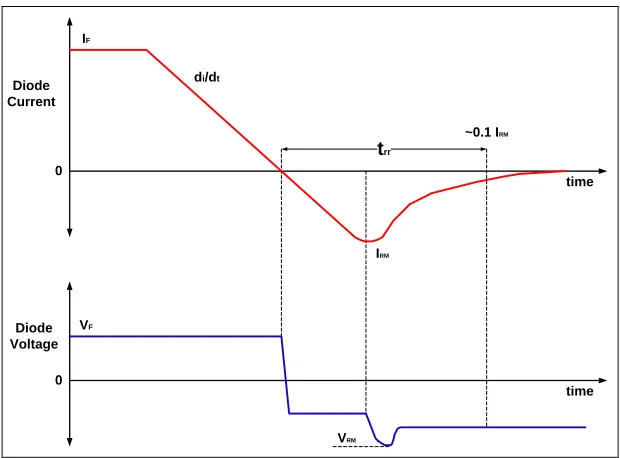
Diode Reverse Recovery Effect
Aside from dead-time loss, the switching elements body diode also experiences what is known as reverse-recovery loss. In a step-down topology, this loss occurs as negative current flows through the body diode during the initial turn-on period of the high-side switch.
In various PWM converters, diodes are utilized to rectify switching voltages and manipulate the flow of current by fly-wheeling and clamping. For silicon carbide (SiC) diodes, the junction capacitance causes a difference in charge distribution whenever the device transitions from a conducting to non-conducting state [13]. This charge difference is dictated by the size of the P-N junction area and it is the main cause of reverse recovery loss. Diodes with larger junction areas result in larger reverse recovery current and thus higher power dissipation during state transitions.
must remain in the same state when the diode makes the transition. Rectifier diodes are typically designed to minimize the time duration of this transition. This is usually referred to as the devices “reverse recovery time”. This reverse recovery time can be used to calculate the transitional losses incurred in a MOSFET by integrating the power across the device. We have
0 rr
t
SW in sw sw in
P
V
V
F
I dt
. (23)The specific transitional power loss during the reverse recovery region can be calculated as
drr rr sw in
P
Q
F
V
, (24)where Qrris the reverse recovery charge; Fswis the switching frequency; Vinis
the input voltage.
IF
di/dt
VF
time
time Diode
Current
Diode Voltage
0 0
trr
~0.1 IRM
IRM
VRM
Figure 2.3: Diode Reverse Recovery Voltage and Current Waveforms
High voltage boost converters require fast and ultrafast rectifiers to minimize the aforementioned reverse recovery losses. There are several methods designers can use to reduce the effect of reverse recovery time shown in Figure 2.3. One method is to minimize the dead-time for when the MOSFET is off and the body diode is forward conducting. A second method is to slow down the synchronous MOSFET turn-on time which decreases the
di dt slope when the diode changes states. A third method, which is more
widely implemented, is to place a high-speed Schottky rectifier diode in parallel with the synchronous MOSFET.
[image:26.612.169.479.87.316.2]source voltage, a positive gate bias is generated by electrons that are injected from under the gate relative to the lateral drift region [15]. Once the threshold voltage of the GaN device is crossed, a conductive channel is formed and the “body diode” conduction effect is established. In comparison to this process, silicon MOSFETs implement diode conduction using minority carriers. These minority carriers are holes that have been injected into the N-side region. When a diode gets reverse biased, it takes time for the minority carriers to be recombined or removed [16]. This process is the main mechanism of reverse recovery loss in silicon MOSFET technologies. Since the GaN process does not implement conduction via minority carriers, the reverse recovery charge is essentially zero. But one disadvantage is that the forward voltage drop of a GaN FET’s “body diode” is higher than that of a comparable silicon technology and so it incurs higher diode conduction losses. However, this disadvantage is easily overcome by utilizing an ultrafast Schottky diode in parallel with the synchronous GaN device.
2.3.
Control Law Design
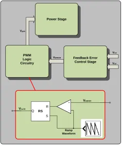
The method of VMC generates a PWM gate drive voltage by comparing an error signal with an internally oscillating ramp waveform. In the simplest of implementations the PWM comparator drives the reset input of an RS latch. Whenever the ramp waveform exceeds the hysteretic limit of the error signal, the RS latch output goes high which turns on the gate of the power-stage MOSFET.
Feedback Error Control Stage
Vref Vout
VERROR PWM
Logic Circuitry
Power Stage
Vref
Vgate
+
-RS
VERROR +
-R
S Q VGATE
[image:28.612.217.468.263.564.2]Ramp Waveform
Figure 2.4:Voltage Mode Control Scheme
1) Two-pole output filter design requires complicated compensation structure at the error amplifier;
2) Control loop gain will vary with input voltage, making it more difficult to ensure stability;
3) Slower dynamic response with regard to line-load disturbances will be experienced because voltage perturbations must be measured at the output before the control loop takes over.
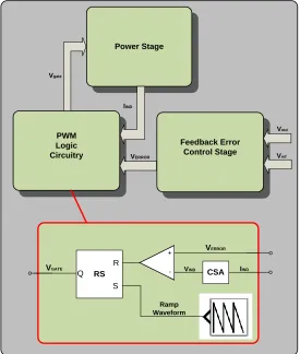
The method of CMC is employed to overcome these disadvantages and it works by implementing the same voltage loop feedback as VMC, but it also includes an inner current loop that is dependent on the average inductor current. Currently there are the followingversions of CMC:
1) Average CMC – Scaled inductor current is converted to a moving average which is used to track a set reference voltage;
2) Peak CMC – MOSFET switches off when the inductor current reaches peak level;
3) Valley CMC – Current is measured on the down slope flowing through low side MOSFET;
In all CMC methods, the inductor current, or low-side switch current, is measured and fed back into a PWM logic comparator. The comparator is typically designed to trip an RS latch whenever the sensed inductor voltage exceeds the level. The specific trip level is dictated by the method of control (peak, valley, average, etc.). Figure 2.8 outlines a basic example of a CMC design.
Feedback Error Control Stage
Vref Vout
VERROR
PWM Logic Circuitry
Power Stage
Vref
Vgate
+
-RS
VERROR
+
-R
S Q
VGATE
IIND
VIND
CSA IIND
[image:30.612.205.480.264.588.2]Ramp Waveform
Both VMC and CMC designs utilize the same compensator design techniques in the feedback error stage. Figure 2.6 shows the typical compensation designs found in most control loops.
Feedback Error Control Stage
+
-Vref Vout
VERROR
RF1
RF2
RC1
CC1
CHF
RC2
Type II Type III
CC2
Figure 2.6:Voltage Mode Feedback Error Control Loop
The compensation method traditionally employed in buck and boost converters is proportional-integral (PI) control. PI control can be implemented using analog or digital methods. The transfer function of an analog Type I PI control law is
2 2
2 1
1
(s) C C
I
C F
sC R H
sC R
. (25)
Modern designs use a parallel capacitor (CHF) to add a high frequency
2
1 2 2 2 1 21 1
( ) C C
II
C HF F C HF
F
C HF
s C R
H s
s C C R C C
s R C C
. (26)
Designs that have widely dynamic input and output conditions may require higher loop bandwidths than can be obtained with Type II compensation. In order to achieve a higher crossover frequency necessary to ensure fast dynamics we must add another pole and zero to the Type II system which provides the additional phase boost necessary to ensure stability. Many SEPIC, Flyback, and buck-boost topologies usually require this type of control. The transfer function is
2
1 2 2 2 1
1 1 1 1
1 2 1 1 1 ( ) 1
C C F
C C
III
C HF F C HF C C
F
C HF
s C R R
s C R
H s
s C C R C C s C R
s R C C
Chapter 3:
Zero-Voltage
Switching
and
Zero-Current Switching Converters
3.1.
Introduction
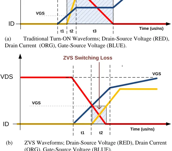
There are various resonant switching techniques designed to mitigate the aforementioned losses incurred in traditional “hard-switching” power designs. Two prominent soft-switching techniques are zero-current switching (ZCS) and zero-voltage switching (ZVS). In this thesis we will be focusing on the more prevalent method of ZVS.
VDS
ID
Traditional Switching Loss
VGS
VGS
t1 t2 t3 Time (us/ns)
VDS
ID
ZVS Switching Loss
VGS
VGS
t1 t2 Time (us/ns)
(a) Traditional Turn-ON Waveforms; Drain-Source Voltage (RED), Drain Current (ORG), Gate-Source Voltage (BLUE).
(b) ZVS Waveforms; Drain-Source Voltage (RED), Drain Current (ORG), Gate-Source Voltage (BLUE).
Figure 3.1: Switching Waveforms Observed in Traditional Hard-Switching (a), and
Soft-Switching ZVS Applications (b) During Switch Turn-on.
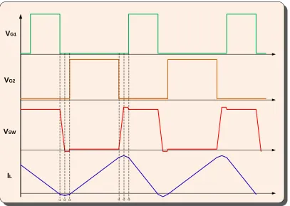
The goal of any ZVS power design is to operate the main power stage switch (or switches) when the drain-source voltage is zero. In practical designs, there is usually some loss encountered during turn-on transition, as the drain-source voltage may not reach zero. Figure 3.2 illustrates the ideal switching waveforms encountered during ZVS operation. VG1 is the gate drive
voltage for the high side synchronous switch, VG2 is the gate drive voltage for
[image:34.612.181.458.151.394.2]inductor current. This circuit behavior will be replicated in PSPICE and validated on an experimental prototype in Chapter 4. For multiphase designs, the waveform behavior remains consistent, but the waveforms for each phase will be offset by a certain percentage. In particular, the waveforms will be offset by 180° for two-phase, 120° for three-phase, 90° for four-phase, etc.
VG1
VG2
VSW
IL
t1t2t3 t1 t2t3
Figure 3.2: ZVS Boost Switching Waveforms
[image:35.612.114.521.266.555.2]converter designs. This is due to the generation of sharp switch-node ringing edges encountered in “hard-switched” designs.
3.2.
Resonant Gate Driving Techniques
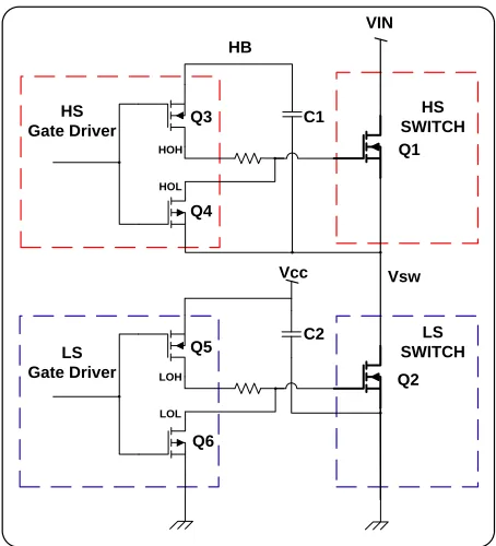
Apart from designing a scheme to implement ZVS in the power stage, there are also techniques to recycle power in the gate-driving circuitry. Figure 3.3 shows a standard gate driving configuration for a synchronous step-down converter. This is the aforementioned “hard-switching” half-bridge design that is known to suffer from heavy losses at high switching frequencies.
LS SWITCH Q3
Q4
Q5
Q6
C1
C2
Q1
Q2 VIN
Vcc HS
Gate Driver
LS Gate Driver
HS SWITCH HB
Vsw
HOL HOH
[image:36.612.210.437.339.589.2]LOL LOH
Figure 3.3: Conventional Gate Driving Scheme for Synchronous Step-down Converters
energy is recovered to drive the power stage on the next PWM transition. It is very effective at reducing the losses when operating at high switching frequencies. Most resonant gate drive designs utilize diodes, inductors and capacitors. These inductors and capacitors are the reactive devices used for power recovery. The idea of utilizing resonant gating is traced back to the 1980’s, and, has been the topic of various research papers in academia and industry.
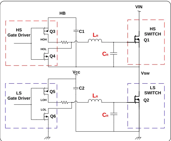
The conventional gating scheme is typically modified by inserting a resonant LC filter at both the low-side and high-side gate locations. The component values are designed to recycle a portion of the power left after each drive cycle.
LS SWITCH Q3
Q4
Q5
Q6
C1
C2
Q1
Q2 VIN
Vcc HS
Gate Driver
LS Gate Driver
HS SWITCH HB
Vsw
LR
CR
LR
CR
[image:37.612.187.488.407.654.2]LOL LOH HOL HOH
The theoretical switching loss in a MOSFET is found by quantifying the gate-drive current used to turn the device on and off. In analyzing the efficacy of a resonant gating scheme, we determine what the gate drive current is while implementing the reactive components as shown in Figure 3.4. The configuration of these components results in a set of second-order LC differential equations;
gateCR LOL R s gate
di
v t V L R i
dt
, (28)
CR
gate R
dv
i C
dt
. (29)
By differentiating (28), we have a second order linear homogeneous equation
2
2 0
gate gate gate
R s
R
d i di i
L R
dt dt C
. (30)
The solution of this differential equation will give us the damping coefficient, resonant frequency, and natural frequency of the gate drive circuit. One has
1 2
( ) t cos( t) sin( t)
gate
i t e A A . (31) The damping coefficient is related to the equivalent series resistance and resonant inductance as
2
s R
R L
The resonant frequency is given by 2 2 1 4 s
R R R
R
L C L
. (33)
The A1and A2 coefficients in (31) must satisfy the initial conditions of
the system. Once the initial conditions are known, A1 and A2 can be found for
by taking the first derivative of (31) and simultaneously solving that system with the original gate current at time t0. We have
2 1
cos( )
1 2
sin( )gate t
di
e A A t A A t
dt
. (34)
We assume that the inductor stores an initial current,IINIT, and the
output capacitor stores an initial capacitor voltage, VINIT. Solving [34] at t 0
gives us the A1 as
1 INIT
A I . (35)
Substituting expression (35) into (34) and solving for A2 at t0 gives
1
2
gate LOL INIT s
INIT
di V V R A
A I
dt L
, (36)
2
LOL INIT s INIT
V V L R I
A L
, (37)
2 2
2
2
1 4
LOL INIT s s
INIT
R R R R
s
R R R
V V R R
I
L L L L
A
R
L C L
2 2 2 4 1 2
LOL INIT s s
INIT
R R R R
R s
R R
V V R R
I
L L L L
A L R L C
, (39)
2
2
2 2 3
4
LOL INIT s init
R s R
V V R I
A L R C
. (40)
3.3.
High Side Gate Driving
Synchronous boost, buck, and buck-boost converters utilize switching elements with floating source connections. The voltage at this source “reference” connection is dependent on the state of the switch, input voltage, output voltage, and output current conditions. This part of the power stage is referred as the “high-side” switch. Proper operation requires specialized gate drive circuitry to maintain appropriate turn-on bias as the source reference voltage varies during each switching cycle.
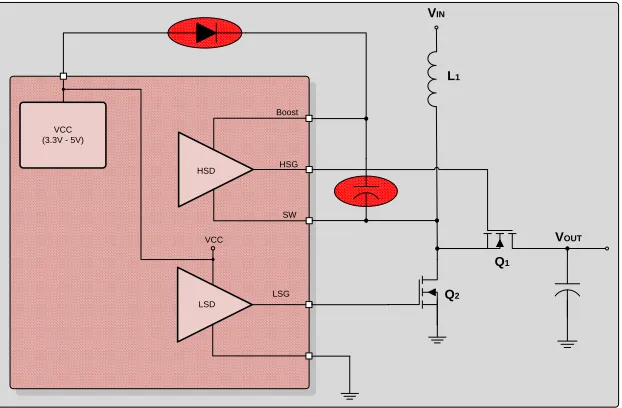
bootstrap diode which is connected to an internal bias supply. Once the switch node is high, the bootstrap diode reverses bias and blocks the capacitor voltage. The capacitor then discharges through the high side driver and provides a floating boost supply. The capacitor must be designed to provide enough energy for the driver to fully turn-on the high side switch during this transition. The bootstrap capacitor is typically in the range of 0.047 F to 0.22 F.
L1
VIN
VCC (3.3V - 5V)
Boost
HSG
LSG SW
VCC HSD
LSD
Q1
Q2
VOUT
Figure 3.5: High Side Bootstrap Circuit in a Boost Converter Application
[image:41.612.188.499.296.500.2]area. The majority of industrial controllers implement this method internally and the designer selects an appropriate diode and capacitor for the end application.
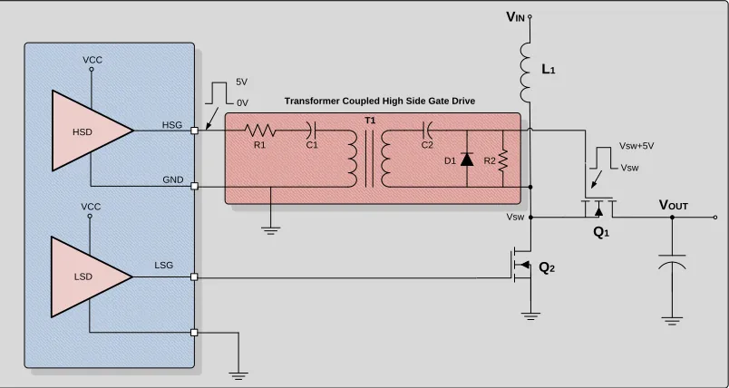
Another simple implementation that achieves a floating gate supply is to use a transformer-coupled driver. Transformers offer noise immunity, isolation, high-speed operation, and enable higher duty cycles. Of the various coupled gate drive transformer designs, one of the more prominent solutions is shown in Figure 3.6. The gate drive design is implemented for a boost converter topology. The design uses coupling capacitors on both sides of the transformer to provide an isolated gate drive voltage that is proportional to the duty cycle of the high-side driving waveform.
L1
VIN
HSG
LSG GND
VCC HSD
LSD
Q1
Q2
VOUT
VCC
0V 5V
R1 C1 C2
D1 R2
T1
Vsw Vsw+5V
Vsw
Transformer Coupled High Side Gate Drive
[image:42.612.115.517.412.626.2]The voltage across the primary side coupling capacitor can be calculated as
1
C D
V V D, (41)
where VD is the high side gate driving voltage from the controller; and D is
the duty cycle of the gate driving waveform
The coupling capacitor provides a reset voltage for the magnetizing inductance of the primary winding. The purpose of this capacitor is to prevent the transformer from saturating [18]. On the secondary side of the transformer, a common DC restore circuit guarantees proper gate drive voltage of the high-side MOSFET. This circuit is composed of another coupling capacitor C2, and a clamping diode D1, which enable operation over duty cycles greater than 85 %.
In designing a transformer-coupled gate drive, the coupling capacitors act as high-pass filters with corner frequencies that are dependent on the input impedance of the output load [18]. The transformer must be designed to achieve impedance matching and voltage isolation. Typically the gate drive transformer is designed as a pulse transformer with fast rise and fall times, minimum overshoot, low leakage inductance, and minimal winding capacitance.
the load as seen by the secondary side of the transformer. This capacitive load can be modeled by the equivalent gate-source capacitance of the high side MOSFET as
G EQ
G
Q C
V
, (42)
where QGis the total gate charge of the MOSFET; and VG is the required
gate-source voltage to turn on the MOSFET.
Ideally the pulse from the high side driving waveform should maintain a rectangular shape as it transfers energy to the secondary side winding. In reality, there is a voltage “droop”. The desired allowable voltage “droop” is used to calculate the transformers magnetizing inductance. The larger the magnetizing inductance is, the lower the percentage of voltage droop as defined by
%
S pw
MAG
R t K
PD
L
, (43)
where K is the coupling coefficient; LMAG is the magnetizing inductance; tpw is
the pulse width of the input voltage waveform; and RS is the input source
impedance to the primary winding
most common core choice in the majority of industrial designs. Once the transformer specifications are developed, and, a suitable device is chosen, we simulate the design in PSPICE to verify theoretical performance. Figure 3.7 shows the realized SPICE schematic used to validate our transformer gate drive specifications.
Figure 3.7:SPICE Schematic for Transformer Coupled Gate Driving
The simulation results confirm a 5 V gate-source driving voltage is achieved at the high-side MOSFET for a boost converter operating at 5 MHz. Figure 3.8 shows the waveform captures of a single PWM pulse. Here, VDis
the initial driving voltage from the controller (~5 V), VSWis the switch-node
voltage for a 10 V to 33 V boost operation, and, VGDis the gate drive voltage
Time
106.040us 106.060us 106.080us 106.100us 106.120us 106.140us 106.160us 106.180us 106.200us 106.220us
1 V(V8:+) 2 V(VSW) V(HGD)
0V 2.00V 4.00V 6.00V 8.00V
-0.85V 9.60V 1
>> 0V 5.0V 10.0V 15.0V 20.0V 25.0V 30.0V
-3.4V 33.6V 2
VSW
VD
[image:46.612.170.503.95.310.2]VGD
Figure 3.8:SPICE Simulation for Transformer Coupled Gate Drive
3.4.
Proposed Digital Zero Voltage Switching Controller
configuration required for all the power stage switching elements, as shown in Figure 3.9.
Digital Controller
COUT
PWM 1
PWM 2
Envelope Command
25V to 40V
L2 30W L1 VG1 VG2 VG1 VG2 VIN VIN DAC DAC DAC DAC ZVS-QSW Soft-Switching Algorithm with Multiphase Delay
= GaN FET EPC8009 = 2929SQ (100nH)
= ~0.047uF
ADC
Output Current (IOUT) Output Voltage (Vout)
Figure 3.9: Block Diagram of Proposed Digital ZVS Two-Phase Converter
3.4.1 Envelope Detection of an Amplitude Modulation RF
Signal
Amplitude modulation (AM) is a radio broadcast technique used to transmit information by combining a baseband message with a carrier waveform. The signal strength of the carrier waveform is typically varied in proportion to the baseband message, encoding the transmitted information.
Shown in Figure 3.10 is the input of an RF PA being routed to an envelope tracking assembly. The first stage of this assembly consists of an envelope detection circuit that demodulates the RF signal. This envelope is then used as an input variable to vary the duty cycle of the PWM drive signals within the envelope tracking power stage.
The bandwidth of an AM signal over a given period is calculated as two times the highest modulating frequency during that time. It is the amount of space within the frequency spectrum that is occupied by the AM signal. For instance, if a 100 MHz carrier is modulated by a 10 MHz message signal, this creates sideband frequencies to appear at 90 MHz and 110 MHz. These sideband frequencies span 20 MHz in the spectrum and thus the bandwidth of the signal is 20 MHz.
Using FIR compiler IP’s, most modern FPGA solutions can easily employ Hilbert transforms that can be used to extract the envelope waveform of an AM signal. But for the majority of applications simple low-pass filtering techniques are sufficient.
RF Power Amplifier
ET MODULATOR Envelope
Detection Circuit
RF IN
[image:49.612.109.534.91.299.2]ENV OUT
Figure 3.10:Envelope Detection Proximity for Envelope Tracking Modulation
Various analog solutions also exist for extracting the envelope of an RF signal. One example is the ADL5511, which is a peak RMS detector capable of extracting RF envelopes with bandwidths up to 130 MHz, and, can operate at input frequencies up to 6 GHz.
3.4.2 Bandwidth Reduction
cost of implementing the proposed ET solution. Various bandwidth reduction techniques have been shown to introduce memory effect distortion into the RF output of the PA which must be compensated by using pre-distortion on the RF input signal [17].
Figure 3.12 displays the extracted envelope for a single tone input AM signal consisting of a 5MHz carrier modified by a 1MHz message signal.
Chapter 4:
Experimental Results and Simulations
4.1.
Introduction
Various MATLAB and PSPICE simulations were performed to evaluate the performance enhancements of a ZVS boost converter. Experimental prototypes were developed to justify our results. The equivalence of simulation and experimental findings confirm the gate charge, gate driving, ZVS boost operation, closed loop control schemes and other major results.
4.2.
Closed Loop Simulations
Figure 4.1:Boost Converter Simulink Schematic
Figure 4.2:Start-up Transient Response of Type II and III Compensators
4.2.1 Inductor Current Sensing
A method for sensing inductor current was developed in [21]. It uses a simple comparator circuit to sense the current across an inductor, and, can be used to provide an amplified voltage to the PWM logic circuit. This method is used in order to maximize system efficiency. Figure 4.4 illustrates the analog circuit used for sensing inductor current.
+
-R1 C1
R2 L1
VIND
V1 V2
IIND
Figure 4.4:Technique for Sensing Inductor Current.
4.3.
Simulation and Modeling of Half-Bridge Gate Drivers
typically provide PSPICE transient models for their components as reported in Table 4.1.
Device Rating RDSon Gate Charge
EPC2015 40V at 33A 3.2mOhm 10.5nC
EPC2020 60V at 60A 2mOhm 16nC
Table 4.1: EPC GaN Devices for Evaluation
For consistent comparison of GaN device, comparable MOSFETs were selected and tested. These devices were chosen from a leading industrial manufacturer using total gate charge as the selection criteria. The devices, documented in Table 4.2, were chosen in order to attain minimal switching losses.
Device Rating RDSon Gate Charge
CSD87350 30V at 30A 2mOhm 20nC
CSD18537N 60V at 54A 11mOhm 14nC
Table 4.2:State-of-the-Art MOSFET Devices for Evaluation
aforementioned devices were developed by manufacturers to fit experimental data.
Figure 4.5 shows the PSPICE schematic used for analyzing the half-bridge driver waveforms for GaN and MOSFET devices.
VDD C11 1U 0 0 LO LO C12 10p HOL C13 10p L3 2.7u 1 2 C14 370u v out R5 10k V14
TD = 100.3u TF = 1n PW = .94u PER = 1.25u V1 = 0 TR = 1n V2 = 5
R6 2 VDD V15 5 U8 D_D1 V16 -250m V17 -250m U9 D_D1 HB C15 .1u V11 V18 20 0 V19 TD = 100u TF = 1n PW = .25u PER = 1.25u V1 = 0 TR = 1n V2 = 5
HI
LM5113 Transient model
U10
LM5113_TRANS THPLH = 28N TLPHL = 26.5N THPHL = 26.5N TLPLH = 28N
HOH HOL HB HI HS LI LOH LOL VDD VSS LO LI GaN FETs
300KHz MOSFET Design Using LM5113 TRANSIENT MODEL 33A, 100V Half-Bridge Gate Driver.
MOSFETS
VDD
300KHz GaN FET Design Using LM5113 TRANSIENT MODEL 33A, 100V Half-Bridge Gate Driver.
C16 1U 0 LO LO 0 + -+ -S9 S VON = 2.6 VOFF = 2.4 ROFF = 1e8 RON = 10m
C17 10p HOL C18 10p L4 2.7u 1 2 C19 370u v out R7 10k V20
TD = 100.3u TF = 1n PW = .94u PER = 1.25u V1 = 0 TR = 1n V2 = 5
+ -+ -S10 S
VON = 2.6 VOFF = 2.4 ROFF = 1e8 RON = 10m R8 2 VDD V21 5 U11 D_D1 V22 -250m V23 -250m U12 D_D1 HB V10 C20 .1u V24 20 0 V25 TD = 100u TF = 1n PW = .25u PER = 1.25u V1 = 0 TR = 1n V2 = 5
HI
LM5113 Transient model
U13
LM5113_TRANS THPLH = 28N TLPHL = 26.5N THPHL = 26.5N TLPLH = 28N
[image:57.612.188.489.214.427.2]HOH HOL HB HI HS LI LOH LOL VDD VSS LO LI U14 csd87330q3d Vin1 1 Vin2 2 TG 3 TGR 4 Vsw3 8 Vsw2 7 Vsw1 6 BG 5 Pgnd 9 HOL
Figure 4.5:PSPICE Schematic for GaN and MOSFET Devices
The schematic model shown in Figure 4.6 was developed to simulate, verify, and analyze the gate charge waveforms for the supplied vendor models. U3 EPC2020 R12 20 V V I R6 20 I1
TD = 100us TF = 1ns PW = 1 PER = 2
I1 = 0 I2 = 1mA TR = 100ns
0 R7 1Meg V20 40V X2 CSD19534Q5A I3
TD = 100us TF = 1ns PW = 1 PER = 2
I1 = 0 I2 = 1mA TR = 100ns
0
R11 1Meg
V22
40V
The drain-source and gate-source voltage waveforms were captured during the turn-on transition region in order to analyze and verify the existence of the “Miller” plateau. Figure 4.7 and 4.8 display the gate charge simulation results for the studied MOSFET and GaN FET respectively.
Figure 4.7:PSPICE Gate Charge Simulation for CSD18537N MOSFET 40V at 2A
4.4.
Experimental Verification of GaN Technology
For the GaN device experiments, two different evaluation platforms were tested: (1) The EPC9001 40 V half-bridge platform shown in Figure 4.9; (2) The EPC9033 60V half-bridge platform shown in Figure 4.10. With the EPC evaluation modules, the power stage still needs to be designed and integrated in order to create a synchronous step-down or step-up converter. The power stage was created as a separate module attachment with each one designed using vector board to achieve approximately 40% inductor ripple current and 50 mVpp output ripple voltage which are typical design specifications for most low voltage buck and boost converters. The power stage module includes input bulk capacitance, output bulk capacitance, and the main switching inductor.
Figure 4.10:EPC9033 60 V Half-Bridge GaN Module.
To validate the manufacturer transient models, an experiment was performed to capture actual gate charge waveforms using a dc current source generator to drive the gate of each device under test. The test setup used to perform this experiment is illustrated in Figure 4.11. These waveforms confirm the simulation results observed in Figures 4.7 and 4.8.
E
20V to 40V
1mA
Electronic Load (250W)
Keithley 2400 Source Meter
Max Current = 5A +
-Figure 4.11:Test Circuit for Capturing Gate Charge Waveforms
[image:60.612.250.436.89.232.2](a) (b)
Figure 4.12:Experimental Gate Charge Waveforms: (a) GaN EPC2020; (b) MOSFET
CSD18537N
The “hard-switching” efficiency degradation for GaN and MOSFET devices were measured at various switching frequencies as specified by the test setup in Figure 4.13. The results in Figure 4.14 show a linear relationship between system efficiency and switching frequency for a 24 W step-down converter. This data was gathered at a 40% PWM duty cycle with Vin = 20 V, Vout = 8 V and Iout = 3 A.
28V
DUT
PWM
Vin
Vout
PC (Matlab) Agilent
PSU Sig Gen
Agilent Electronic Load
(30W) +
-Figure 4.14: GaN and MOSFET Efficiencies at 24 W Output Power for Various Switching
Frequencies
As the MOSFET devices are not recommended to operate at high frequencies, the switching losses for these devices were tested up to 1800 KHz as indicated by the dashed line in Figure 4.14.
(a) (b)
Figure 4.15: 24 W Half-Bridge GaN Step-down Converter at (a) 2 MHz and (b) 300
KHz.
incorporating two enhancement mode MOSFETs within a single device package size [2]. One example of this is TI’s NexFET™ PowerStack™ technology. This device uses very low resistance copper clips fabricated on the die to connect the high-side source to the low-side drain in order to ensure minimal CSI effects. Figure 4.16 shows TI’s graphical outline of this packaging method.
[image:64.612.225.461.263.388.2]Figure 4.16: TI NexFET™ Power Block Technology Dual MOSFET Package
Figure 4.17: TI NexFET™ Power Block™ Evaluation Platform TPS53819
the aforementioned Power Block™ design to the results obtained from using GaN FETs. The outcome will define the advantages of GaN technology, and, show that clever MOSFET packaging techniques may overcome the cost disadvantage of current GaN devices for certain applications. Figure 4.17 shows the NexFET™ switching platform that is used for evaluation and comparison of the studied GaN devices. Circled in red is the dual MOSFET package in a 5x6mm SON footprint area.
The initial efficiency measurements are taken under the typical nominal load conditions under which industrial manufacturers usually report performance data. The following experiment was performed to evaluate the efficiency performance across the entire operating envelope. We measure performance metrics under various input and output conditions. The three variables are the output voltage Vout, output current Iout, and input voltage
Vin. The output voltage variable is treated as static. The system is designed
to regulate this Vout variable to a constant 8 VDC. We then evaluate the
efficiency performance as a surface function guided by the dynamic relationship between output current Iout and input voltage Vin.
Figures 4.18 and 4.19 show the efficiency surface plots in 3D at 300
blue-green surface represents data gathered for the CSD87350 platform. At ~0.6 A the outputs of the two surface plots intersect. The intersection line represents the input/output load conditions where the EPC9033 GaN design begins showing improvement over the CSD87350 MOSFET design. The GaN devices only provide better efficiencies at higher output power levels (>6 W). At low output load conditions, the MOSFET achieves better efficiency performance.
Figure 4.18: 300 KHz Efficiency Surface Plots of EPC9033 (Yel-Pk) vs. CSD87350 (Blu-Grn)
reasonable amount of time, EPC GaN technology may not be an appropriate solution. If the design is consistently operating at high output powers, the improvement in efficiency is ~4-8 % at output currents greater than 2 A.
Figure 4.19:900 KHz Efficiency Surface Plots of EPC9033 (Yel-Pk) vs. CSD87350 (Blu-Grn)
4.5.
Simulation and Modeling of a Zero Voltage Switching
Boost Converter
operated using the transformer coupled gate drive method discussed in Section 3.3.
VSW1
VG2
VG1
IL1
VSW2
VG4
VG3
[image:68.612.110.538.147.403.2]IL2
Figure 4.20: PSPICE Schematic for ZVS 2-Phase Boost Converter
Time
106.00us 106.02us 106.04us 106.06us 106.08us 106.10us 106.12us 106.14us 106.16us
1 V(U1:GATEIN) V(C4:2) 2 V(VSW) 3 -I(L2)
0V 4.0V 8.0V -1.2V 1 >> 0V 20V 40V 60V 2 0A 2.0A 4.0A -1.0A 5.0A 3
1 V(U2:GATEIN) V(V8:+) 2 V(VSW2) 3 -I(L3)
[image:69.612.112.536.92.375.2]0V 4.0V 8.0V -1.2V 1 SEL>> 0V 20V 40V 60V 2 0A 2.0A 4.0A -1.0A 5.0A 3 SEL>> P h a s e 1 P h a s e 2 VSW1 VG1 VG2 IL1 VSW2 VG3 VG4 IL2
Figure 4.21: PSPICE Simulation of ZVS Boost Converter.
4.6.
Experimental Results for a ZVS Boost Converter
For the experimental prototype, various EPC GaN FETs were evaluated in a boost configuration at different switching frequencies. The design specifications for the experimental prototype are reported in Tables 4.3 and 4.4.
Parameter Value Units
Vin 12 V
Vout 30 V
Iout 1 A
Fsw 5 MHz
[image:69.612.240.409.580.662.2]Parameter Part Number Description
L1 2222SQ-161J 160 nH RF Inductor
Q1-Q4 EPC8009 60 V 2.7 A GaN FET
C1-C4 06031A101JAT2A 100 pF Ceramic Capacitor
U1 UCC27611DRV High speed gate driver
[image:70.612.123.525.305.547.2]M1 PFD2014 Gate Drive Transformer
Table 4.4: Input/Output Boost Component Identification
The experimental prototype was fabricated using standard FR4 material using four PCB layers. Figure 4.22 shows the top and bottom sides of the populated PCB and the associated layout routing design.
Figure 4.22: 30W Multiphase ZVS Boost Converter Prototype and Layout Design
operating under ZVS conditions at 1 MHz and 3 MHz, respectively, at ~15 W output power.
Figure 4.23: ZVS Boost Converter Switching Waveforms at 1 MHz
[image:71.612.165.483.431.653.2]The efficiency improvement between the ZVS boost converter and a traditional hard-switched boost converter is shown in Figure 4.25. The ZVS operation provides from 6% to 10% efficiency improvement over standard hard-switched configurations.
Figure 4.25: Efficiency Curves Comparing ZVS vs. Hard-switched Boost Converter.
4.6.1 Closed Loop System and Frequency Response
and tested against the simulation experiments from Section 4.5. Figures 4.26-4.27 display the loaded and unloaded transient response plots for the ZVS step-down converter operating at 500 KHz and 1 MHz, respectively. A stepped electronic load of 3 A is applied to the system to classify the dynamic performance.
Closed loop control was employed using a third order compensator. The digital compensators are realized using an IIR filter with coefficients that can be tuned in real-time to allow for direct comparison and evaluation. The discrete time difference equation for the compensator structure is given as
0 1 2
( ) ( 1) ( ) y( 1) ( 2)
u k u k b y k b k b y k . (44)
[image:73.612.108.541.412.578.2](a) (b)
Figure 4.26: Optimized Transient Response for Digital Step-Down Converter Operating at
(a) (b)
Figure 4.27: Optimized Transient Response for Digital Step-Down Converter Operating at
1MHz with 3A Output Loaded (a), and, Unloaded (b), Under Type III Compensation.
One of the advantages of using a digital controller is the ability to obtain frequency response data. Since the compensator is implemented digitally, frequency response measurements can be taken without the need for acquiring an external network analyzer. The control law coefficients can be updated in real-time allowing direct evaluation of parameters. Various control law compensators including Type I, Type II, and Type III can be evaluated simply by updating code builds.
margin. The design coefficients were programmed into the MCU and then the frequency response for the compensated closed loop system was captured.
Figures 4.28 and 4.29 report the pole/zero placement design parameters. These feedback coefficients were used to achieve stable operation for the 500 KHz and 1 MHz designs.
Figure 4.28: Pole Zero Placement Coefficients for 500KHz Frequency Response
Figure 4.29: Pole Zero Placement Coefficients for 1MHz Frequency Response
Figure 4.30: Magnitude and Phase Frequency Response Plots for 500 KHz Operation
Figure 4.31: Magnitude and Phase Frequency Response Plots for 1 MHz Operation
4.7.
Conclusion
4.7.1 Summary
This thesis examines various topics in the design, analysis, and application of high performance industrial DC/DC converters. A method of achieving resonant power conversion by controlling the discontinuous/continuous mode boundary is implemented and examined using an experimental hardware prototype.
In Chapter 1, the theoretical framework, relevant to the loss mechanism for typical synchronous step-up and step-down converters is discussed. The main causes for switching losses are studied. An understanding of these fundamental topics is critical to realizing hardware designs that improve performance, transient response, effi