Article
Active On-Chip Dispersion Control Using a Tunable
Silicon Bragg Grating
Charalambos Klitis1 , Marc Sorel1and Michael J. Strain2,* 1 School of Engineering, University of Glasgow, G12 8LT, UK
2 Institute of Photonics, Department of Physics, University of Strathclyde, G1 1RD, UK
* Correspondence: [email protected]
Received: 26 July 2019 ; Accepted: 24 August 2019; Published: 28 August 2019
Abstract:Actively controllable dispersion in on-chip photonic devices is challenging to implement compared with free space optical components where mechanical degrees of freedom can be employed. Here, we present a method by which continuously tunable group delay control is achieved by modulating the refractive index profile of a silicon Bragg grating using thermo-optic effects. A simple thermal heater element is used to create tunable thermal gradients along the grating length, inducing chirped group delay profiles. Both effective blue and red chirp are realised using a single on-chip device over nanometre scale bandwidths. Group delay slopes are continuously tunable over a few ps/nm range from red to blue chirp, compatible with on-chip dispersion compensation for telecommunications picosecond pulse systems.
Keywords:silicon photonics; dispersion control; Bragg gratings
1. Introduction
Integrated Bragg grating filters are an established and widely used technology on the Silicon-on-Insultor (SOI) material platform. They are applied in a large variety of applications, including, optical filtering [1,2], sensing [3], laser cavity feedback [4] and all-optical signal processing [5,6]. A wide range of device geometries have been demonstrated in order to exercise control over the grating optical characteristics, namely the filter bandwidth [7], ripple [8], extinction and dispersion [2,9,10]. In turn, the optical characteristics of the grating can be designed through the coupling coefficient, κ, and the grating Bragg wavelength, λB ,as a function of the propagation length [10,11]. Active control of Bragg grating devices has also been demonstrated using multi-section p-n junction elements to create tunable notch features in the device stopband [12].
The control afforded by the Bragg grating device over the dispersion of a propagating signal is crucial in applications such as all-optical signal processing [5] and pulse shaping [13]. Commonly, the group delay profile of a device is varied through the local Bragg wavelength function. Therefore, by simply varying the grating period [14], or effective waveguide index, devices can be created with linear and higher order dispersion profiles [9] or even complex multi-band filter designs [15]. Filter ripple effects have been effectively minimised by suitably apodising the gratingκ along its length [9,10,16]. The dispersion profile of a grating device is generally defined during the fabrication procedure as a modulation of the period [14] or effective index [17]. Some rigid tunability of the device spectrum has been demonstrated through global thermal [18] or electronic tuning [19]. Narrowband delay has also been demonstrated using multi-section gratings at the band-edge [20,21]. However, for future Photonic Integrated Circuits (PICs), true tunable dispersion on-chip will be a valuable component functionality. The principle of reconfigurable silicon photonic circuits has been well established in devices including ring resonators [22], Mach–Zehnder interferometers [23,24], and modulators [25], using both thermo-optic and carrier injection methods.
In this work, we present the design considerations for realising tunable dispersion gratings on the silicon photonics platform and present measured performance of fabricated devices. Control is demonstrated producing both red and blue chirp in a single device over bandwidths and group delay ranges compatible with picosecond pulse compensation schemes.
2. Results
2.1. Actively Tunable Bragg Grating Design
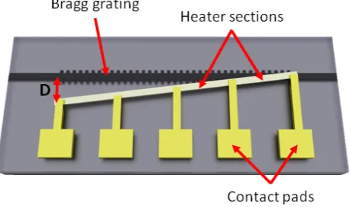
[image:2.595.171.423.256.405.2]The Bragg grating device is implemented with a constant Bragg wavelength,λB(z), along its length. To create a chirp in the grating response, the Bragg wavelength function is controlled by creating a thermal gradient along the device length. A schematic of the device is shown in Figure1.
Figure 1.Schematic of a Bragg grating with an integrated heater element. The displacement between the waveguide axis and heater central position is a function of propagation length, with a maximum displacementD.
Figure 2.(a) FEM thermal model of a heater element co-axial with a silicon-on-insulator waveguide; and (b) calculated temperature of the silicon waveguide as a function of offset of the heater central axis from the central axis of the waveguide.
In Figure1, a signal injected from the left hand side of the device would see an increasing refractive index with propagation length through the grating, and therefore an effective red chirp. Alternatively, light coupled in from the right hand side of the device would see decreasing refractive index with propagation length and, therefore, effective blue chirp. The magnitude of the induced chirp is dependent on the grating length, coupling coefficient and thermal gradient. The difference in temperature and, therefore, refractive index, along the grating can be controlled electronically through the power dissipated in the heater.
To demonstrate the tunable dispersion concept, a grating response was chosen to cover bandwidths of≈1 nm, and group delays in the picosecond range, corresponding to typical dispersion compensation requirements for picosecond telecommunications pulses. The gratings were designed on a silicon-on-insulator platform with a core layer thickness of 220 nm and a mean waveguide width of 500 nm. The grating period,Λ0, was set at 318 nm, to give a Bragg wavelength around 1550 nm.
The grating was designed with a length of 250µm and a sinusoidally varying sidewall amplitude modulation,d, of 6 nm. The grating perturbation is realised as a sinusoidal variation around an average waveguide width,w. A schematic of the sidewall perturbation grating is shown in Figure3along with a SEM image of the fabricated device before deposition of the upper-cladding.
Figure 3.(a) Schematic of a sinusoidal sidewall perturbation Bragg grating, and (b) SEM image of a fabricated device.
[image:3.595.130.461.546.683.2]is the local modal refractive index andΛ0is the grating period, the grating chirp can be modelled
using a variation in refractive index. The modal index is in turn dependent on the temperature at the waveguide generated by the local heater element. The heater element is fabricated using a 900 nm wide track of 50 nm thick NiCr. To create a linear chirp profile, the displacement,D(z), between the centre lines of the waveguide and heater element, is varied using az0.5relationship. It is worth noting that the waveguide dispersion of silicon nanowire waveguides is significant [31], and therefore must be taken into consideration when designing and modelling Bragg gratings in silicon.
[image:4.595.92.513.352.508.2]Figure4a shows a measured transmission spectrum of the fabricated device with no power dissipated on the heater, i.e., the device is unchirped. Measured device spectra can be fitted to the TMM model using a least squares curve fitting method. In this case, the form of the grating chirp is assumed, e.g., unchirped or linear blue-chirp. The coupling coefficient and the maximum and minimum effective index values at the grating ends are then left as free parameters to perform the fit. The extracted modal index from the fitting of the unchirped grating is 2.4386 and the coupling coefficient is 323 cm−1. Furthermore, since an apodisation scheme based on variation of the grating sidewall amplitude was employed, residual ripples in the grating reflectivity and group delay spectra are still apparent. Grating coupling coefficient apodisation schemes that more effectively reduce the spectral ripple of the device, and can be fabricated within nanometric tolerances, have recently been demonstrated using phase based methods [10,16].
Figure 4. (a) Measured and fitted Bragg grating transmission spectra of the grating device in the unchirped state; and (b) measured grating spectra for increasing power dissipation, PD, on the thermal heating element.
To assess the effects of the heater on the z-dependent modal index, the grating transmission spectrum was measured as a function of total electrical power dissipated on the heater element,PD. Figure4b shows the measured transmission spectra, linearly varyingPDup to 47.3 mW. The grating fitting was carried out in each case, assuming a linearly varying modal index as a function of the propagation length, with extreme modal index values as free parameters. The local shift of the Bragg grating along the device can be decomposed into two components: a baseline shift of the full device since the full length sees some minimum thermal increase, and a relative temperature change along the propagation direction due to the displacement of the heater section. This can be approximated as:
λB(z) =2(neff,0+dnmin+dn(z))Λ0 (1)
whereneff,0is the effective modal index of the grating waveguide at room temperature,dnminis the
increase in modal effective index at point of greatest displacement between the waveguide and the heater element, anddn(z)is the additional thermal increase along the grating length abovednmin
dnminanddn(z)maxfrom the transmission spectra. As s expected,dn(z)maxhas a higher gradient as
[image:5.595.203.390.128.281.2]a function ofPDthandnmin, indicating the effective chirping of the grating response.
Figure 5.Variation in minimum and maximum thermally induced modal refractive index shifts of the device extracted from fitting of the transmission spectra.
2.2. Group Delay Chirp Control
Figure6shows the calculated reflectivity spectra and group delay profiles for the grating, with the extracted values ofdnminanddn(z)maxas parameters. The group delay is only calculated for the
[image:5.595.94.515.404.555.2]portion of the reflectivity spectrum above 90% of its maximum value.
Figure 6. (a) Simulated reflectivity; and (b) group delay of a Bragg grating device with thermally induced refractive index differences as parameters.
chirp rate is less than the blue chirp rate achievable at similar power dissipation levels, at bands further detuned from this wavelength.
Figure 7.Simulated group delay bands as a function of dissipated power on the heater centred at: (a) 1551 nm; and (b) 1552.2 mn.
The group delay of the fabricated tunable grating was measured as detailed in Section 5. Figure8
shows the measured group delay as a function of power dissipated on the heater.
Figure 8.Measured group delay tuning as a function of dissipated power on the heater.
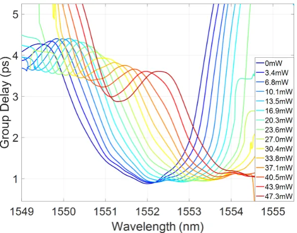
[image:6.595.145.444.374.608.2]Figure 9.Measured group delay bands as a function of dissipated power on the heater centred at: (a) 1551.7 nm; and (b) 1553 mn.
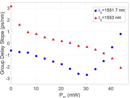
[image:7.595.180.408.337.510.2]Figure10presents the average group delay slope for both sub-bands in Figure9. In both cases, quasi-continuous tuning of the group delay slope is demonstrated in the ps/nm range, with both blue and red chirp accessible from a single device and from a single injection direction.
Figure 10.Measured group delay slope as a function of dissipated power on the heater corresponding to the dispersion bands centred at 1551.7 nm; and 1553 nm.
3. Discussion
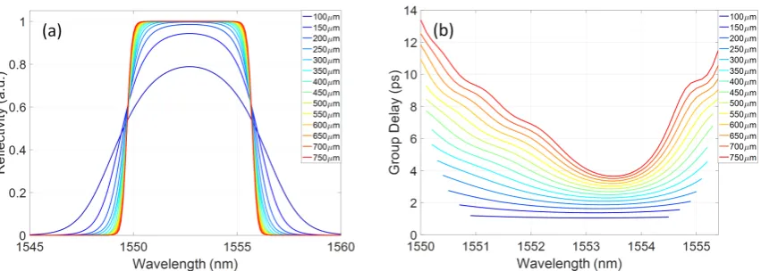
Figure 11. Simulated grating: (a) reflectivity; and (b) group delay spectra with grating length as a parameter.
The group delay range across the spectrum is, as expected, dependent on the grating length. Therefore, devices can be designed based on the required application requirements.
In addition to the relative group delay dispersion induced across the device, the absolute spectral position of the grating response is dependent on two main factors. The first is related to fabrication tolerances in the manufacture of the device. Since the absolute Bragg wavelength of a fixed period grating is proportional to its effective modal index, any variation from the design geometry will lead to a shift in the resultant Bragg spectrum. However, in high resolution fabrication schemes such as optimised electron beam or deep ultraviolet (UV) lithography, such variations are global rather than local. That is, the average waveguide width may vary from run to run, or even between spatially separated devices, but is unlikely to see significant variation across a single device. Typical geometrical variations can be in the nanometre range, leading to effective index variations in the order of 10−3–10−2 [33]. The second factor affecting the absolute spectral position of the Bragg grating response is the global thermal shift experienced by the full grating when the heater is electrically driven. The thermal element induces both a global wavelength shift of the grating characteristic and a local gradient to induce the chirped profile, as detailed in Figure5, The global, or minimum index, shift experienced by the full grating is in the order of 10−3, comparable with any potential geometric effects. To implement control over both the group delay slope and central wavelength, a second heater element could be implemented parallel to the Bragg grating. This element would produce a rigid index shift of the full grating response, shifting the demonstrated group delay curves in wavelength. Therefore, using both heater controls, varying group delay slopes in both chirp directions could be accessed at a single central wavelength, as long as the un-heated grating central Bragg wavelength was designed to be at a shorter wavelength than the required application space.
4. Conclusions
5. Materials and Methods
5.1. Device Fabrication
The devices were fabricated on a 220 nm thick silicon core on a buried oxide lower cladding layer of 2µm. The patterns were written using e-beam lithography into hydrogen silsesquioxane (HSQ) resist that was subsequently used as a hardmask for Inductively Coupled Plasma (ICP)-Reactive Ion Etching (RIE) etching of the silicon. Polymer spot-size convertors [34] were fabricated to match the input lensed fibre mode to the waveguides. The final devices were coated with a 900 nm thick silica uppercladding before definition of the heater elements and electrical transmission lines. The heaters were fabricated as 900 nm wide strips of 50 nm thick NiCr. Multiple point contacts on the heater lines were defined to reduce the necessary voltage required to drive the device, as shown in the schematic of Figure1. The heaters were divided into 50µm long sections, each with a resistance of≈1.5 kΩ, and were driven in an alternating positive/ground, arrangement.
5.2. Transmission and Group Delay Measurements
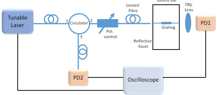
[image:9.595.120.475.341.496.2]The Bragg grating devices were probed using a tunable laser coupled through fibre polarisation optics and a lensed fibre tip to the chip, as shown in Figure12.
Figure 12.Transmission and group delay measurement setup. (Pol., polarisation; PD, photodiode).
Figure 13.(a) Measured reflectivity spectrum of the grating with no induced chirp; and (b) detailed spectrum of the Fabry–Perot fringes created by the intereference between the device bar facet and grating reflector.
Author Contributions:Conceptualisation, M.S. and M.J.S.; Funding acquisition, M.S. and M.J.S.; Methodology, C.K. and M.J.S.; Software, M.J.S.; Writing—original draft, C.K. and M.J.S.; and Writing—review and editing, C.K., M.S. and M.J.S.
Funding:This research was funded by EPSRC grant numbers EP/P013597/1, EP/P013570/1, and EP/L021129/1.
Acknowledgments:The authors acknowledge the support of the James Watt Nanofabrication Centre staff.
Conflicts of Interest:The authors declare no conflict of interest.
References
1. Harris, N.C.; Grassani, D.; Simbula, A.; Pant, M.; Galli, M.; Baehr-jones, T.; Hochberg, M.; Englund, D.; Bajoni, D.; Galland, C. Integrated Source of Spectrally Filtered Correlated Photons for Large-Scale Quantum Photonic Systems. Phys. Rev. X2014,4, 041047, doi:10.1103/PhysRevX.4.041047.
2. Oser, D.; Mazeas, F.; Le Roux, X.; Pérez-Galacho, D.; Alibart, O.; Tanzilli, S.; Labonté, L.; Marris-Morini, D.; Vivien, L.; Cassan, É.; et al. Coherency-Broken Bragg Filters: Overcoming On-Chip Rejection Limitations. Laser Photonics Rev.2019, 1800226, doi:10.1002/lpor.201800226.
3. Prabhathan, P.; Murukeshan, V.M.; Jing, Z.; Ramana, P.V. Compact SOI nanowire refractive index sensor using phase shifted Bragg grating. Opt. Express2009,17, 15330–15341.
4. Zhang, C.; Srinivasan, S.; Tang, Y.; Heck, M.J.R.; Davenport, M.L.; Bowers, J.E. Low threshold and high speed short cavity distributed feedback hybrid silicon lasers. Opt. Express2014,22, 10202–10209, doi:10.1364/OE.22.010202.
5. Burla, M.; Cortés, L.R.; Li, M.; Wang, X.; Chrostowski, L.; Azaña, J. Integrated waveguide Bragg gratings for microwave photonics signal processing. Opt. Express2013,21, 25120–25147, doi:10.1364/OE.21.025120. 6. Rutkowska, K.A.; Duchesne, D.; Strain, M.J.; Morandotti, R.; Sorel, M.; Azaña, J. Ultrafast all-optical
temporal differentiators based on CMOS-compatible integrated-waveguide Bragg gratings. Opt. Express
2011,19, 19514–19522.
7. Wang, X.; Shi, W.; Yun, H.; Grist, S.; Jaeger, N.A.; Chrostowski, L. Narrow-band waveguide Bragg gratings on SOI wafers with CMOS-compatible fabrication process. Opt. Express2012,20, 15547–15558.
8. Veerasubramanian, V.; Beaudin, G.; Giguere, A.; Le Drogoff, B.; Aimez, V.; Kirk, A.G. Design and Demonstration of Apodized Comb Filters on SOI. IEEE Photonics J. 2012, 4, 1133–1139, doi:10.1109/JPHOT.2012.2204971.
9. Chen, G.F.R.; Wang, T.; Donnelly, C.; Tan, D.T.H. Second and third order dispersion generation using nonlinearly chirped silicon waveguide gratings. Opt. Express 2013, 21, 29223–29230, doi:10.1364/OE.21.029223.
10. Cheng, R.; Han, Y.; Chrostowski, L. Characterization and compensation of apodization phase noise in silicon integrated Bragg gratings. Opt. Express2019,27, 9516–9535, doi:10.1364/oe.27.009516.
12. Zhang, W.; Yao, J. A fully reconfigurable waveguide Bragg grating for programmable photonic signal processing.Nat. Commun.2018,9, 1396, doi:10.1038/s41467-018-03738-3.
13. Rivas, L.M.; Strain, M.J.; Duchesne, D.; Carballar, A.; Sorel, M.; Morandotti, R.; Azaña, J. Picosecond linear optical pulse shapers based on integrated waveguide Bragg gratings.Opt. Lett.2008,33, 2425–2427. 14. Tan, D.T.H.; Ikeda, K.; Saperstein, R.E.; Slutsky, B.; Fainman, Y. Chip-scale dispersion engineering using
chirped vertical gratings. Opt. Lett.2008,33, 3013–3015.
15. Strain, M.J.; Thoms, S.; MacIntyre, D.S.; Sorel, M. Multi-wavelength filters in silicon using superposition sidewall Bragg grating devices. Opt. Lett.2014,39, 413–416, doi:10.1364/OL.39.000413.
16. Cheng, R.; Chrostowski, L. Apodization of Silicon Integrated Bragg Gratings through Periodic Phase Modulation. IEEE J. Sel. Top. Quantum Electron.2019,26, doi:10.1109/JSTQE.2019.2929698.
17. Kim, M.s.; Ju, J.J.; Park, S.K.; Lee, M.H.; Kim, S.H.; Lee, K.D. Tailoring Chirp Characteristics of Waveguide Bragg Gratings Using Tapered Core Profiles. IEEE Photonics Technol. Lett.2006,18, 2413–2415, doi:10.1109/LPT.2006.886132.
18. Giuntoni, I.; Stolarek, D.; Kroushkov, D.I.; Bruns, J.; Zimmermann, L.; Tillack, B.; Petermann, K. Continuously tunable delay line based on SOI tapered Bragg gratings. Opt. Express2012,20, 11241–11246.
19. Khan, S.; Baghban, M.A.; Fathpour, S. Electronically tunable silicon photonic delay lines. Opt. Express2011, 19, 11780–11785.
20. Jiang, L.; Huang, Z.R. Integrated Cascaded Bragg Gratings for On-Chip Optical Delay Lines. IEEE Photonics Technol. Lett.2018,30, 499–502, doi:10.1109/LPT.2018.2801026.
21. Chung, C.J.; Xu, X.; Wang, G.; Pan, Z.; Chen, R.T. On-chip optical true time delay lines featuring one-dimensional fishbone photonic crystal waveguide. Appl. Phys. Lett. 2018, 112, 071104, doi:10.1063/1.5006188.
22. Zheng, X.; Patil, D.; Lexau, J.; Liu, F.; Li, G.; Thacker, H.; Luo, Y.; Shubin, I.; Li, J.; Yao, J.; et al. Ultra-efficient 10 Gb/s hybrid integrated silicon photonic transmitter and receiver. Opt. Express2011,19, 5172–5186, doi:10.1364/OE.19.005172.
23. Orlandi, P.; Morichetti, F.; Strain, M.J.; Sorel, M.; Bassi, P.; Melloni, A. Photonic Integrated Filter with Widely Tunable Bandwidth.J. Light. Technol.2014,32, 897–907.
24. Pérez, D.; Gasulla, I.; Crudgington, L.; Thomson, D.J.; Khokhar, A.Z.; Li, K.; Cao, W.; Mashanovich, G.Z.; Capmany, J. Multipurpose silicon photonics signal processor core. Nat. Commun. 2017, 8, 636, doi:10.1038/s41467-017-00714-1.
25. Reed, G.T.; Mashanovich, G.; Gardes, F.Y.; Thomson, D.J. Silicon optical modulators. Nat. Photonics2010, 4, 518–526, doi:10.1038/nphoton.2010.179.
26. Atabaki, A.H.; Eftekhar, A.A.; Yegnanarayanan, S.; Adibi, A. Sub-100-nanosecond thermal reconfiguration of silicon photonic devices. Opt. Express2013,21, 18312–18323, doi:10.1364/OE.21.015706.
27. Densmore, A.; Janz, S.; Ma, R.; Schmid, J.H.; Xu, D.X.; Delâge, A.; Lapointe, J.; Vachon, M.; Cheben, P. Compact and low power thermo-optic switch using folded silicon waveguides. Opt. Express2009, 17, 10457–10465.
28. Dong, P.; Qian, W.; Liang, H.; Shafiiha, R.; Feng, D.; Li, G.; Cunningham, J.E.; Krishnamoorthy, A.V.; Asghari, M. Thermally tunable silicon racetrack resonators with ultralow tuning power. Opt. Express2010, 18, 20298–20304, doi:10.1364/OE.18.020298.
29. Orlandi, P.; Morichetti, F.; Strain, M.J.; Sorel, M.; Melloni, A.; Bassi, P. Tunable silicon photonics directional coupler driven by a transverse temperature gradient.Opt. Lett.2013,38, 863–865.
30. Yamada, M.; Sakuda, K. Analysis of almost-periodic distributed feedback slab waveguides via a fundamental matrix approach.Appl. Opt.1987,26, 3474–3478, doi:10.1364/ao.26.003474.
31. Turner, A.C.; Manolatou, C.; Schmidt, B.S.; Lipson, M.; Foster, M.a.; Sharping, J.E.; Gaeta, A.L. Tailored anomalous group-velocity dispersion in silicon channel waveguides. Opt. Express 2006, 14, 4357–4362.
32. Sahin, E.; Ooi, K.J.; Png, C.E.; Tan, D.T. Large, scalable dispersion engineering using cladding-modulated Bragg gratings on a silicon chip. Appl. Phys. Lett.2017,110, doi:10.1063/1.4982157.
34. Roelkens, G.; Dumon, P.; Bogaerts, W.; Van Thourhout, D.; Baets, R. Efficient silicon-on-insulator fiber coupler fabricated using 248-nm-deep UV lithography. IEEE Photonics Technol. Lett.2005,17, 2613–2615, doi:10.1109/LPT.2005.859132.
35. Skaar, J. Measuring the group delay of fiber Bragg gratings by use of end-reflection interference.Opt. Lett.
1999,24, 1020–1022.
c