Abstract: In the present evolving technology, an Automated Optical Inspection is a solution for identifying the various types of defects occurring in assembled PCB with SMT components. As these high-end machines are expensive, moreover the small scale industries can’t afford such a huge investment, in this paper a low cost image processing technique where a good known reference image is compared with the acquired image is being tried. This work provides an automated approach for identifying few of the defects related to the SMT components found in the assembled PCB, using three different techniques namely Contour Analysis, Optical Character Recognition and Pixel Subtraction for identifying shifted components, value of the components and missing components respectively in LabVIEW platform. The time taken for identifying the various defects through different techniques are calculated and tabulated. Using these techniques the number of errors can be decreased in turn the end performance can also be enhanced with the increased production yield.
Keywords: Assembled Printed Circuit Board (PCBA), Automated Optical Inspection (AOI), Optical Character Recognition (OCR), Surface Mount Technology (SMT).
I. INTRODUCTION
Printed Circuit Board is a backbone of all of the electronic products used in various sectors such as Automotive, Medical, Aerospace, and Defense etc. Manufacturing of complete PCB involves two processes i.e. manufacturing of Bare PCB and manufacturing of assembled PCB. The manufacturing processes for both are unique and follow their own stages. Assembling of electronic components onto the bare PCB plays a major role and is application specific. Each stage in the assembly process possesses its unique steps and are defined based on design specifications of the end product. In the proposed work components related to Surface Mount Technology (SMT) is the main area of concentration in the assembling process of PCBA. Thus the detailed information regarding SMT is explained in the further section.
II. MANUFACTURING PROCESSOFASSEMBLEDPCB A. SMT assembling process
Surface Mount Technology (SMT) is an advanced component assembling technique, where the components are placed on the top of the bare PCB which serves as a mounting point and is based on design parameters. This technology has helped in
Revised Manuscript Received on October 05, 2019.
Anitha D B, ECE Department, VVIET and Research Scholar, MRF, Mysore, India. Email: [email protected]
Mahesh Rao, ECE Department, MIT, Mysore, India.
Email:[email protected]
reduction of PCB size, MTBF, etc. Thus in order to achieve the proper and efficient placement of the SMT components on the PCB pad involves various processes which require advanced and high-end machines. The major process flow of the SMT [1, 2] is explained in brief which is shown in Fig 1.
Fig 1: SMT process flow
Baking: Baking is a process of removing any moisture contents present in the bare PCB and is compulsorily for class 3 products.
Screen Printing: Screen Printing is a process in which solder paste is applied on pads of bare PCB through the stencil. Then the applied paste is inspected to make sure it present only on pads.
Pick & Place: Pick and place is a very important and crucial process in SMT, where the SMT components are picked and placed in specific defined locations on the PCB pads by automated robotic machines.
Reflow: Reflow is the next processes involved in the SMT, at this stage the solder paste will be melted to firmly attach the placed components on the PCB.
Automated Optical Inspection (AOI): AOI is inspection tools which are involved in the detection of various errors found in the previous process.
B. Common Errors involved in SMT process
Different types of errors specific to components are observed and these errors possess different implications on different tests. Thus it is necessary to identify these errors. The major errors [3,4] are listed and are explained in brief 1.Component Shift: The components will move or shift
from the actual positions that they are specified and is replaced by a different valued component.
2.Wrong Value: Instead of placing a specified value of the component different valued components are mounted. 3.Component Missing: Sometimes the components are
skipped or not mounted on particular locations.
4.Component Value Erase: It is observed when the value of mounted component on the board is erased or not visible. 5.Upside Mount: The components are mounted upside
down.
SMT Component Inspection in PCBA’s using
Image Processing Techniques
6.Pin Bend: This type of defects are found when some of the IC pins are bent
7.Tomb Stoning: Tomb Stoning also known as chip lifting. When one end of the chip component will be detached from the copper pad of the PCB and stand on another end of the chip component.
8.Component Damage: Assembled components are not working or that are damaged.
9.Component Polarity: The components are placed in the wrong direction.
Among these errors, only first three errors are identified in the proposed work. Each type of error identification possesses different methods and the previous works done on the selected techniques are studied and are explained in brief.
III. LITERATURE SURVEY
An automatic visualized inspecton system [5] is used for fault identification of the assembled PCB. Different techniques are used for detecting the defects such as missed components, wrong polarity, and breaks in circuits. Specifically, fault-detection method involves the conversion of RGB to Gray, thresholding, Bit-wised XOR operation on the reference & test image. Then contour analysis technique is used for training and labeling the obtained defects that result in identifying the defects. Further canny edge detection technique is applied. Finally, the resultant image obtained with the highlighted name of the faulted components.
The authors [6] have made an estimated study on different automated defect detection techniques for inspecting the PCBs. The morphological segmentation of image is extracted to expect the maximum identification of defects in PCB image, this result in increased speed and accuracy. Initially the source image is captured in full color then it is converted into gray scale. Various filtering methods are applied to remove noise, the histogram view of the resultant image is stretched and equalized to fine tune it. Then wavelet transform and subtraction of images are implemented to identify the defects. They concluded that the specified technique performs faster compared to other techniques.
Sonal Koushik and Javed Ashraf [7] proposed a system for finding the faults in PCB image using image subtraction method. Initially, the template image and test image is selected then XOR logical operation is applied for both the images. Later the machine vision PCB inspection model is employed by subtracting the test PCB from the template PCB. Then defected portion is highlighted in the obtained resultant image. Thus the obtained resultant image is subjected to thresholding operation, which is then analyzed practically and validated between the images.
The authors [8] have successfully experimented for detection of defects by applying template matching, background subtraction, and wavelet transform algorithms. They found the identification of misaligned component by using background subtraction algorithm. In this, the RGB image is converted into HSV and then it is converted to gray image. The median filter is applied to the gray image by tracing the boundary region and then in the resultant binary image the defect has been detected. For template matching algorithm the image is converted into gray scale image, then for both the images normalized cross correlation is calculated. Next, by combining the defect has been detected. Later for detecting the upside placed component, the median filter is
applied by the conversion of the RGB format of PCBA image to gray. The difference in the images is identified and morphological operation is performed for finding the defects by applying the wavelet transform technique.
In order to identify the errors of SMT components, few algorithms were examined based on geometry and shape features, module matching and detection of components in assembled PCB. This paper [9] uses some inspection techniques such as template matching, pyramid algorithms, and patch analysis for the 2-Dimentional images of various defects in SMT components such as missing, shift polarity and reverse placement. The inspection times for all these are different and that has been noted. Finally, they concluded that three factors are effectively influencing the inspection and they are precision, efficiency, and minimum similarity degree. Therefore it can be proved that the proposed methods can satisfy the requirements of high stability, reliability, precision and inspection speed in defect detection for surface mounted devices of assembled PCB.
The contour Analysis technique is used for defining the specific regions around the image. This is encrypted using a group of complex numbers. In a selected contour, the first point itself leads to last point vector, which is scanned and the offset for each vector is defined by complex numbers that are x+iy. The x+iy specifies the offset values of selected vectors, where x specifies a particular point on x-axis and y specifies a particular point on the y-axis. The offset is dependent on the previous vectors thus it is defined in terms of complex numbers [10-13].
In the current digital world, an OCR technique is widely spread across many areas in banks, business fields, research fields IT fields, etc., for example, recognition of the Patterns in the images, Computerized Visions, Invoices, Automatic License Plate Recognition, computer-receipts etc. [14-17].
Thus this survey covers different methodologies involved in the previously done works. Few of the ideas of these works are significantly considered in the present work for detecting the various defects occurring in the assembling process of SMT components.
IV. IMPLEMENTATION
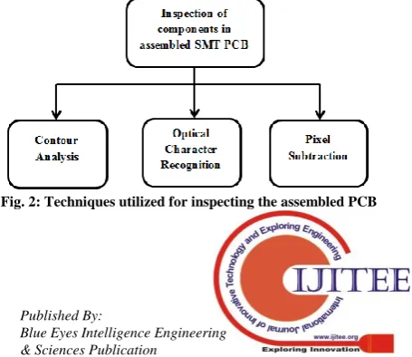
[image:2.595.322.550.636.833.2]The defects related to the assembled SMT PCB’s are unique, also differs based on their size and shapes of components. In order to get 100% defect free production from the SMT, it is necessary to examine the PCBA. In the proposed work three major techniques are applied for identifying few of the defects related to the SMT components in the assembled PCB and they are represented in Fig 2. These techniques are tried to implement through Lab VIEW environment.
A. Contour Analysis Technique
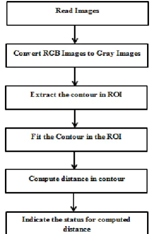
To identify the shifted components the Contour Analysis technique is applied. The flow diagram for identifying the shifted components is shown in Fig.3. The program flow starts by extracting and reading the images from the specifically defined path and these images are converted from RGB image to grayscale.
The best contour values from the reference image are extracted and ROI (Region of Interest) is predefined along the contour values in the image. Next, the values of target image contours are compared with the template contour. If there is a difference found with the fitted contour values, then it is referred as defective image and the status is indicated using Boolean Control as a component status display in the front panel window of LabVIEW. Thus for inspecting the shifted components in PCBA, two images are considered and both are subjected to test. For example, the selected test images containing chip resistors mounted on PCB, which is then converted from RGB image to gray scale levels which are shown in Fig 4.
[image:3.595.304.550.225.376.2]Any variations with respect to the defined contour regions are identified then the corresponding image will be considered as a defective one and the status specific to this inspection is represented by glowing Red LED. The final inspection of the defective image is represented in front panel window of LabVIEW which is shown in Fig 5.
Fig 3: Flow diagram for identifying the shifted components
In a similar way if there are no variations with respect to the defined contour regions then the resultant will be considered as no shift and the status is indicated by glowing Green LED, the resultant window of this is shown in Fig. 6. Therefore by matching the contour regions, the shifted component defect is identified successfully.
Fig 4: RGB and gray scale levels of test images for Contour Analysis technique
B. Optical Character Recognition Technique
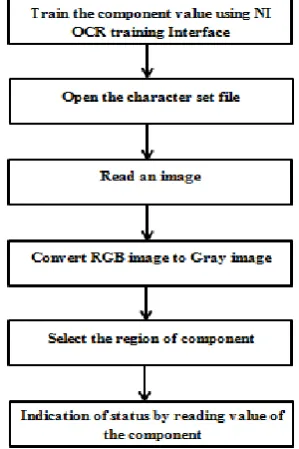
[image:3.595.96.248.363.600.2]In the proposed work an idea of OCR technique have been deployed for recognizing the value of component in assembled PCB. This means, while mounting a correct component it might have placed different valued component. Even the value of the component is also important in placement of the SMT components which may affect at testing or leads to improper working of end product. For inspection, out of the whole panel only a zone is considered to identify the values of particular components. The value of particular component to be inspected is trained using NI OCR Training Interface of NI LabVIEW. The training of component values is shown in Fig 7.
Fig 5: Status indication of defective image using Contour Analysis technique
Fig 6: Status indication of good image using Contour Analysis technique
The different steps involved in training the component values are
Step 1: Open the NI OCR Training Interface window. Step 2: Select the required images
Step 3: In training section set “ train single character button”
Step 4: Draw a rectangular region in the component area
Step 5: Adjust the training parameters
Step 6: Enter the correct value or string in the “correct string” list box
[image:3.595.305.549.399.555.2] [image:3.595.66.273.691.760.2]The trained character set file is retrieved from the specified path. Then select a test image, which should be converted from RGB to Gray scale. Further, select a component region for inspection and corresponding status will be displayed using 2-Boolean controls. The flow specific to this is shown in Fig 8. The Sample set 1 and Sample set 2 are the two set of images considered for inspecting the values of components in assembled PCB. The considered images are converted into gray scale and are verified separately. These image sets are shown in Fig 9 and Fig 10 respectively.
Fig 7: Training the values of the component
Fig 8: Flow diagram for identifying the component values
[image:4.595.91.241.368.593.2]Fig 9: RGB and gray scale levels of sample 1 test images for OCR
Fig 11: Status indication of sample 2 good image using OCR technique
For indicating the recognized values two LED’s are used, one is for indicating the correct value of the component and the other is for indicating the wrongly valued component. Further, the read value of the component is displayed and if the read string matches the fed value the LED named “Correct Value” will glow which is shown in Fig 11.
Fig 12: Status indication of sample 2 defective image using OCR technique
Otherwise, if the read value is not matched with the fed value the LED named “Wrong Value” will glows up. The overall time taken for the inspection have displayed and the time taken for identifying the value of the component have also displayed in the front panel window, which is shown in Fig 12.
C. Pixel Subtraction
In this proposed system a pixel subtraction method is used for identifying missing components. This is employed using NI LabVIEW software and the flow diagram for finding the missed components is shown in Fig 13. Initially, both the reference image and the test images are considered. Both the images are in color, which is
converted from RGB image to the array of pixel values.
[image:4.595.305.550.435.593.2] [image:4.595.69.280.628.702.2]Further, the pixel values of the defective image or test image are subtracted from the pixel values of Good or Reference image.
[image:5.595.308.545.151.423.2]In order to inspect the missed components, a simple image pixel subtraction method is deployed in the program. Here the same program is applied for the different set of images. Both the Good and defective images different sets is shown in Fig 14 (a) & (b) and Fig 15 (a) & (b) respectively.
Fig 13: Flow diagram for identifying the component Missing defect
Fig. 14: Sample 1 Test images for Pixel Subtraction
The front panel inspection windows of different sample 1 test images are shown in Fig 16. For this, the whole PCB panel has been considered. In this PCB it has its 9 sub-panels. The presence of all the components is considered as the good board or good image and in other board, few of the components are missing. In each sub-panel, Quad Flat Package (QFP) and IC is missing. Along with these two, a component namely GSM modem is also missing in 2nd, 3rd,
6th and 9th sub-panels. After subtraction, the components position is highlighted in the resultant image.
[image:5.595.93.243.170.493.2]In a similar way in the sample set 2 the images, the good image contains all the components, but in the defective image 3 components namely an Inductor, Crystal and an IC is missing. After subtraction, the resultant image is obtained with highlighting the defective portion. The front panel inspection windows of different sample 2 test images are shown in Fig 17.
[image:5.595.309.545.451.593.2]Fig 15: Sample 2 Test images for Pixel Subtraction
Fig 16: Front panel window of Pixel subtraction for Sample 1 Images
Fig 17: Front panel window of Pixel subtraction for Sample 2 Images
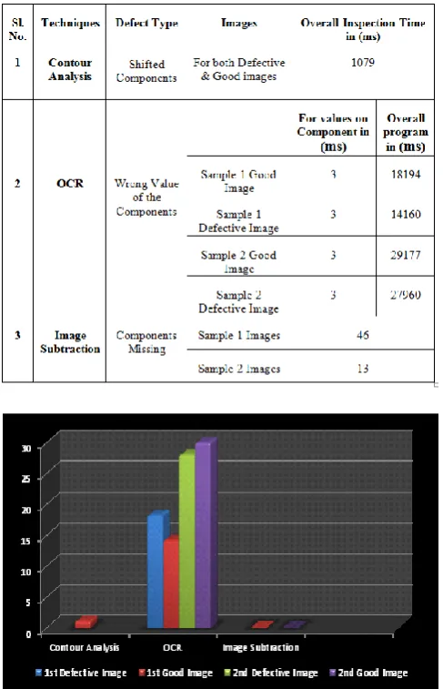
By summarizing all the results of different techniques using LabVIEW platform, the overall time taken for inspecting different PCBA images are tabulated as in the Table -I. This shows the time difference between the different techniques for different images. Initially using contour analysis technique for both the images fed from a saved folder is 1079ms.Then for OCR technique, the inspection time will depend on the selection of saved character set file and the images. For the first & second good images, it takes 18194 ms and 29177ms respectively. Similarly, for the first & second defective images, it takes 14160ms and 27960ms respectively. By noticing that, for all type of
[image:5.595.47.290.530.660.2]Finally, for Image subtraction technique the timing differs from the sample set 1 of PCBA image and the sample set 2 of PCBA images. An image containing a number of components with its sub panel the inspection time is 46ms. As well as for a small panel with few components it takes only 13ms. The timing difference is represented graphically and is shown in the Fig 18.
Table- I: Inspection time for different PCBA images using Different Techniques
Fig 18: Graphical representation of Inspection time for different techniques.
V. CONCLUSIONANDFUTUREENHANCEMENT
Some industries may have the high-end machines such as AOI and AXI, to inspect the assembled PCBs only at the final stage. In order to rework the detected defects of assembled components more time is needed, thus in turn production will be quite slow. If few errors related to components are detected and corrected before Reflow process, it will results in less rework time and increased production time. Thus in order to install or incorporate the same machine, again it is a matter of cost and space. Apart from these existing machines, this image processing technique be a low-cost alternative with a simple camera and one computer can be easily implemented. The proposed work mainly affirms on inspecting few of the defects related to the assembled SMT components using few of the techniques namely Contour Analysis, OCR and Pixel Subtraction methods for identifying the defects such as shifted
components, placement of wrongly valued components and missing components respectively. Inspection time for detecting the various defects through different techniques are tabulated and represented graphically. Using these approaches the numbers of defects can be reduced as well as the end performance can also be enhanced with the increased production yield. For inspecting missed components it takes very less time compared to other defects whereas OCR it depends on the selection of files, also both can be applied to many other boards. Apart from these two, the shifted component program works for only a defined board because it depends on ROI.
Only three types of defects have successfully identified by concentrating on a small part of the PCBA image. One can try this with the full board and also for other types of defects.
ACKNOWLEDGEMENT
Author express their sincere gratitude to Mr. Sharath K Bhatt, Business Development VP, Kaynes Technology India Pvt. Ltd., Mysuru. The authors also wish to extend their gratitude to Mr. S.Chiranjeevi, DGM (PCB&F), ITI, Bangalore and Mr. Amulya Mohapatra, Member Technical, Indian Printed Circuit Association, Bangalore for their technical input to carry out this research. Finally, Authors also appreciate the support of Maharaja Research Foundation, Mysore.
REFERENCES
1. http://www.surfacemountprocess.com 2. http:// www.smtnet.com
3. http://www.electronicsandyou.com
4. http://www.blog.optimumdesign.com\most-common-pcb-assembly-defects
5. Rasika R Chavan, Swathi A Chavan, Gouthami D Dokhe, Mayuri B Wagh and Archana S Vaidya, “Quality Control of PCB using Image Processing” International Journal of Computer Applications (0975-8887), Volume 141- No. 5, May 2016.
6. Mohith Borthakur, Anagha Latne and Pooja Kulkarni, “A comparative study of automated PCB Defect Detection Algorithms and to Propose an Optimal approach to Improve the Technique” International Journal of Computer Applications (0975-8887), Volume114-No, 6, March 2015. 7. Sonal Kaushik and Javed Ashraf, “Automatic PCB Defect Detection
using Image Subtraction Method”, International Journal of Computer Science and Network (IJCSN), Vol. 1, Issue 5, Oct 2012.
8. Ganavi V M and Dr. Mahesh Rao, “Printed Circuit Board Assembly Defects Detection using Image Processing Techniques”, IJESE 2016. 9. Xibing Li and Jianjia wang, “Defect detection of SMT Electronic
Modules” An International Journal of Applied Mathematics & information Sciences 7, No. 2, 515-520 (2013).
10. www.codeproject.com\contouranalysis-for-image-recognition-in-c 11. Ann Abraham Babu, Satish Kumar Varma and Rupali Nikhare, “Hand
Gesture Recognition System for Human Computer Interaction using Contour Analysis” International Journal of Research in Engineering and Technology, Volume 04, Issue 03, March 2015.
12. Jitendra Malik, Serge Belongle, Thomas Leung and Jianbo Shi, “Contour and Texture Analysis for Image Segmentation, International Journal of Computer Vision 43(1), 7-27, 2001.
13. Mrs. Namratha and S Mandvikar, “Augmented Reality using Contour Analysis in E-Learning” International Journal of Innovative Research in Science, Engineering and Technology, Vol. 2, Issue 5, May 2013. 14. www.wikipedia.org\Optical-character-recognition
15. Aruna Panda, Prof. Mishra SN and Prof. Das, “An Advanced LabVIEW based OCR system for Hand Written Scripts” International Journal of Multidisciplinary Research and Development, Volume 3, Issue 2, February 2016, Page No. 01-05.
16. Dilpreet Kaur Dhillon, Preethi Bansal and Karmjit Singh, “ An Interactive Speech Synthesis
Computer Engineering, Volume 4, Issue 5, 2013.
17. Jasvinder Kaur and Monika Aggarwal, “A LabVIEW Approach to Detect the Theft of Indian Currency Notes” International Journal of Advanced Research in Electronics Electronics Communication Engineering (IJARECE), Volume 2, Issue 1, January 2013.
AUTHORSPROFILE
Anitha D B B.E, M.Tech, Associate Professor, Department of ECE, VVIET, Mysore. Currently Pursuing Ph.D. in Maharaja Research Foundation recognized by University of Mysore,
India. Research interests include Signal and
Image processing.
Mahesh K Rao B.E., M.A.Sc., Ph.D. (USA), Professor and Head, Department of ECE, MIT, Mysore. Published several papers in International and National journals. Research interests include image processing and computer vision, Wireless Sensor Networks.