Abstract: Organic Light Emitting Diode i a firm condition lights tools. Where as, the charge carriers are given from the anode and cathode. In this paper, we proposed our cutting-edge method with different doping concentration of the substance in Organic Light Emitting Diode (OLED). Additionally, we increase the performance of OLED devices and deliberate their execution augmentation using exploiting dissimilar doping. The performance of OLED depends upon various factors like thickness of material, doping, band gap and many more. In this paper, one parameter i.e. doping concentration that affect the performance is studied and analyzed. For simulation purpose, 2D numerical simulations using finite element method by device simulation software silvaco ALTLAS by silvaco Inc. is used. And simulation result shows that on increasing doping in hole transport layer, it increases luminance power. At a doping concentration p-type impurity of 1018, maximum luminance power 9.99x10⁻⁵ W/μm is obtained and maximum current is 4.99μA.
Index Terms: Doping, Emissive layer, Hole transport layer, Organic materials.
I. INTRODUCTION
From past few decades, OLED is a commonly used in straight light discharging modern technology, which is constructed using developing a sequence of organic thin films amongst two conductors i.e. cathode and anode. When the electrical current is executed on the terminals, a bright light is released. Several of the considerable organic lots sources are emissive layers (EML), hole injection layer (HIL) and electron injection layers EIL), Hole transport layers (HTL), electron transport layer(ETL), hole blocking layers (HBL) and electron blocking layer (EBL) [1]. OLED's consists of several attributes. Some of the unique attributes are transparency, versatility, as well as slimness which are used to advise ingenious potential for various propose and function. On another hand, the price per lumen needs diminishing for hostile through predictable light sources. The presentation of the tool is increased by the method of growing light elimination. The supplementary expense of light elimination is cheap [3].
Organic light-emitting diode (OLED) is a firm-condition device which is significantly dissimilar in manifestation and lights presentation from light-emitting diodes (LEDs). OLED
Revised Manuscript Received on December 22, 2018.
Abhilasha, Department of Electronics and Communication Engineering, JECRC University, Jaipur, INDIA.
Prof. K. M. Singh, Department of Electronics and Communication Engineering, JECRC University, Jaipur, INDIA.
plates have enormous visual putting in jeopardy like floor tiles, flexible plates for illumination encounters without glare, display screens and lightening devices. Comparable to tiles, we used to develop designs, straight or arrayed round preparations, or unsystematic model to promote straight or think about the eye. OLED is integrated an architectural part for given to build words or humorous model or maintain method exploration in construction [2].
For fabrication of OLEDs, different types of organic electroluminescent materials are used: SMOLED (Small molecule OLED) and PLED (polymer LED) [8]. The color of discharged light depends upon the shade of photon produced by electroluminescent organic molecule; it is a feature of energy difference between HOMO (Highest occupied molecular orbit) and LUMO (Lowest unoccupied molecular orbit). A reduced energy barrier is needed corresponding to HOMO level of emissive material to acquire high hole injection rate from the anode. As a result, a high work function anode is required to acquire this purpose. Similarly, for effective electron injection from the cathode, a low electron barrier is required with respect to LUMO level of organic material. Therefore, a low work function material meets the requirement of cathode material. For that reason, the cathode materials are chose as low work function materials while anode materials are taken as high work function materials [5].
Several technologies are used to design OLEDs and most commonly used technologies are AMOLED (active matrix organic light emitting diode) and PMOLED (Passive matrix organic light emitting diode). PMOLEDs have organic layers and strips of anode that are arranged perpendicular to the cathode strips. Lights are emitted through pixels. Pixels are formed by the intersections of the cathode and anode strips. In PMOLED, the intersection point of this layer is known as pixel. The brightness of each pixel is directly proportional to the amount of applied current. External circuitry applies current to selected strips of anode and cathode, determining which pixels get turned on and which pixels remain off. PMOLEDs are cheap and easy to design and fabricate. But due to use of external circuitry, they consume more power (mainly due to the power needed for the external circuitry). AMOLEDs have full layers of cathode, organic molecules and anode. The anode layers have a thin film transistor (TFT) plane in parallel to it so as to form a matrix. So each pixel can individually ON or OFF as per choice. This helps in switching each pixel, thus forming an
image. Hence, the pixels switch off whenever they are not required or there is a
Performance Analysis of OLED by Variation of
Doping in Hole Transport Layer
black image on the display, hence AMOLED consume less power than PMOLED, this helps in increasing the battery life of the device [12].
The display of OLED derived from module devices that
include organic electroluminescent material (built through petite molecules or polymers). If electricity prompted the display Screen, after that it releases the light. Generally, an OLED incorporates completing layer and an emissive layer, which put among two electrodes are set down on a substrate simultaneously. The accomplishing layer is prepared by organic molecules that convey "gap" from the anode. The emissive layer is a layer of the organic compound which transfer electrons from the cathode and discharge light to an electric current. In the emissive layer, the light color is relying on the category of organic particle. Producer situate many kind of organic films on a similar OLED to construct create displays screens [4].
OLED is mainly utilized to decrease the depth like a film and connect with the OLED for illumination and display function. The depth of organic thin films includes hundreds nm, the grooved arrangement developed near to the device which gravely affects the electrical individuality of OLED [6]. In LEDs, the depth of quantum barriers (QBs) is determined as an effective direction to limit effectiveness sag. The consequence of QB depth on the effectiveness sag for LEDs is still deliberated controversially. The performance sag is significantly hidden by means of dropping the QB depth [7].
There are several variables that influence efficiency and performance of an OLED. These elements include work function of anode and cathode, band gap and conductance of organic material, doping of organic material, doping strength, thickness of organic material, anode voltage, electric field.
Two categories of photo physical devices are a) Photometric (it can recognize by eyes) and also b) Radiometric (It includes physical properties such as: no. of photons, energy of photon, optical power, luminous intensity, electric field, anode current) . Recombination rate in an OLED relies on numerous elements as doping profile and thickness of material. On increasing concentration of dopant, conductivity increases.
II. DEVICE STRUCTURE
In this section, we have simulated two multilayer device including Alq3 [Tris (8-hydroxy quinolinato) Aluminium] and
TPD (N,N‟-bis (3-methylephenyl)-N,N‟-diphenyl-benzidine) sandwiched between electrodes. Alq3 layer is working as
emissive layer (EML) and TPD layer is used as hole transport layer (HTL). The first model is stimulated using EML layer and HTL layer only. And for second device, the same model is stimulated using doping of P-type dopant. In addition, the doping of P-type polymer film is done with concentration of 1x1016 cm-3 in hole transport layer. For this purpose, doping of BCP (2,9-dimethyl-4,7-diphenyl-1,10-phenanthroline) is done in device 2. All the organic materials used to design device A and device B are electroluminescent substance. It stimulated phenomenon of luminance when electricity is applied. The thickness and design description for device A and device B are as given:
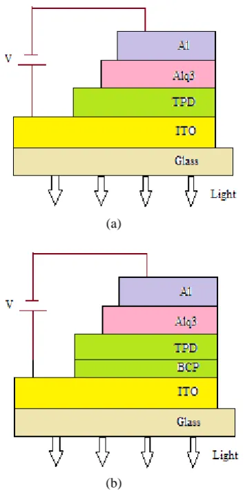
Device A: Al (100nm)/ Alq3 (50nm)/ TPD (40nm)/ ITO (120nm)
Device B: Al (100nm)/ Alq3 (50nm)/ TPD (40nm)/ BCP/ ITO (120nm)
Device A is undoped device and device B is BCP doped TPD device. The geometrical model of the device structure is shown in fig 1.
(a)
[image:2.595.349.527.148.504.2](b)
Fig 1. Device structure of OLEDs (a) undoped
device (b) BCP doped device
ITO is chosen as anode due to its high work function and good transparency and cathode material is Al. The cathode material is chosen as low work function material such as Mg and Ca. but these materials are very sensitive to moisture leads to reduce its lifetime. Therefore, more stable materials like Al or compound materials are used as cathode. The work function of ITO is 4.7eV and work function of cathode is 2.9 eV [11]. The base material for both the device is glass due to its transparency. Plastic material can be chosen instead of glass material to design flexible OLED. Light is drawn out from anode terminal.
(b)
[image:3.595.97.258.64.281.2](c)
Fig 2. Molecular Structure of (a) Alq3 (b) TPD (c) BCP
organic materials
[image:3.595.296.558.66.172.2]The Molecular structures of all the used organic materials are shown in Fig 2. [10]
Table I: Properties of materials used in OLED
Materials Refractive Index n
Extinction Index k
Thickness (in nm)
Al 0.867 6.42 100nm
Alq3 1.655 0 50nm
TPD 1.7 0.2 40nm
BCP 1.6 0.1
Doping concentration of
1x1016 cm-3
Table I shows material properties like thickness, refractive index and extinction index [9]. Extinction index is defined as the capacity of a material to absorb light at a given wavelength per mass density.
III. RESULTS AND DISCUSSIONS
The simulation of device A and Device B is done using
simulation software Silvaco TCAD software. This segment
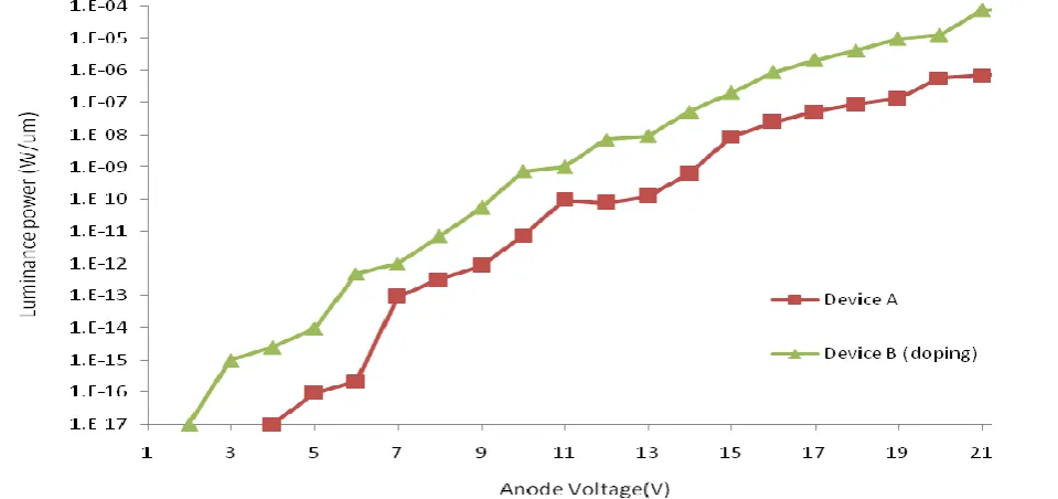
explains about the consequence and conversation regarding a variety of doping of the organic material which obtained in OLED device. The comparison curve of device A(undoped device) and device B (BCP doped TPD device) is drawn between maximum luminance power and anode voltage, as shown in fig 3.
Fig 3. Luminance power-Anode voltage for the device A and device B
From fig 3 it is clear that luminance power is much high for device B as compared to device A and also turn ON voltage is reduced when doping is done. Therefore, Device B shows
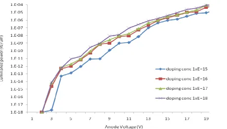
[image:3.595.69.549.371.597.2]Fig 4. Luminescent Power vs. Anode Voltage for Different Doping Concentration in TPD Layer
So from fig 4 it is accomplished that the change in doping concentration in hole transport layer encompasses a straight consequence of device presentation through maintaining the flow of charge transporter in the course of the natural layer. It leads to increase luminance power.
To understand the effect of doping concentration of active material on device performance, doping concentration in the range of 1015 to 1018 cm3 is taken for simulation, and from the simulation, performance parameters like: maximum luminescent power, maximum current and maximum internal power are extracted and analyzed.
Table II. Effect of concentration change of BCP doped TPD on Performance Parameter
Active Organic Material
Doping Concentration
of p-type in active material
Turn On voltage
Maximum luminance power
Pmax
Maximum current Imax (μA)
TPD
1015 2.9 2.17x10⁻⁵ 1. 09
1016 2.6 8.86x10⁻⁵ 4.43
1017 2.5 9.90x10⁻⁵ 4.95
1018 2.3 9.99x10⁻⁵ 4.99
Table II illustrate the effect of change in doping concentration in hole transport layer. From the table, it is observed that turn on voltage reduced when doping concentration increases. Hence device turns ON by applying low power supply. It leads to increase battery life.
IV. CONCLUSION
In OLEDs; the emissive electroluminescent layer is a layer of natural intensifies which is used to release illumination on applying an electric current. In this research paper, we use two type of multilayer OLED; one with different doping concentration in hole transport layer and another without any doping concentration. Then we draw the following conclusion:
a) P-type doping in HTL layer increases luminance power at same anode voltage, and turn on voltage reduces when doping is done.
b) On increasing doping concentration, improved luminance power is obtained. It further leads to increases quantum efficiency of OLED.
The purpose of this paper is to analysis the influence of doping in hole transport layer. And simulation results mention that doping increases the efficiency of an OLED.
The future work may include, taking different type of organic electroluminescent material of different thickness and varying doping concentration. And by comparison best suitable material may be identified.
REFERENCES
1. Riedel, Daniel, et al. "Polymer-based scattering layers for internal light extraction from organic light emitting diodes." Organic electronics 32 (2016): 27-33.
2. Mallesham, Godumala, et al. "Phosphine oxide functionalized pyrenes as efficient blue light emitting multifunctional materials for organic light emitting diodes." Journal of Materials Chemistry C 3.6 (2015): 1208-1224.
3. Noguchi, Yutaka, et al. "Charge carrier dynamics and degradation phenomena in organic light-emitting diodes doped by a thermally
activated delayed
4. Li, Wei, et al. "Dual n-type units including pyridine and diphenylphosphine oxide: effective design strategy of host materials for high-performance organic light-emitting diodes." Chemical Science 7.11 (2016): 6706-6714.
5. B. geffroy, P. L. Roy and C. Prat, “Review: Organic light Emitting diode (OLED) technology: Materials, devices and display technologies”, Polymer International 55, pp. 572-582, (2006). 6. Rhee, Sang Ho, et al. "Correlation between interlayer thickness and
device performance in blue phosphorescent organic light emitting diodes with a quantum well structure." Organic Electronics 42 (2017): 343-347.
7. Kim, Sung-Jin, et al. "Efficient green OLED devices with an emissive layer comprised of phosphor-doped carbazole/bis-oxadiazole side-chain polymer blends." Organic Electronics 12.3 (2011): 492-496 8. N.T Kalyani and S.J. Dhoble, “Organic light emitting diode: Energy Saving lighting technology- A review”, renewable and sustainable energy reviews 16, (2012), pp:2696-2723.
9. W. J. Yang, C. K. Hu and T. T. Li, “ Investigation of surface Plasmon enhanced organic light emitting diode by numerical analysis”, international conference 2015 china semiconductor technology, Shanghai, China(2015).
10. B. Changdong, Z. Fanghuli and L. Yanfei, “Influence of Alq3: C545T on luminescence of blue LED”, Second international conference on Digital manufacturing and automation, 2011, pp. 641-643.
11. I. Farjamtalab, A. Kashaniniya, R. N. Sabbaghi, “Analyzing the influences of work function anode on the performance of OLED”, IOSR journal of electrical and electronics engineering, vol 10, issue 5, (2015), pp 131-135.
12. Sambandan, S. andNathan, A., „Single-Technology-Based Statistical Calibration for High-Performance Active-Matrix Organic LED Displays‟ IEEE Transactions on Journal Of Display Technology, 3(9), pp. 284-294,(2007).
AUTHORS PROFILE
Abhilasha is a Ph.D. Scholor in department of Electronics and computer Engineering. She has done his M.Tech and B.Tech from Mody University, Lakashmangarh, INDIA. Her areas of expertise are optoelectronics devices and VLSI design. She has published over 18 peer reviewed papers in prestigious journals and peer reviewed conference proceedings.