promoting access to White Rose research papers
White Rose Research Online [email protected]
Universities of Leeds, Sheffield and York
http://eprints.whiterose.ac.uk/
This is an author produced version of a paper published in Physical Review B.
White Rose Research Online URL for this paper:
Published paper
Butler, K.T., Vollum, P.E., Muggerud, A.M., Cabrera, E., Harding, J.H. (2011) Structural and electronic properties of silver/silicon interfaces and implications for solar cell performance, Physical Review B, 83 (23), Article number: 235307
BB11467
REVIEW COPY
NOT FOR DISTRIBUTION
Structural and electronic properties of silver/silicon interfaces
and implications for solar cell performance
Keith T. Butler,1 Per Erik Vullum,2 Astrid Marie
Muggerud,3 Enrique Cabrera,4 and John H. Harding1
1
Department of Materials Science and Engineering, University of Sheffield, Mappin Street, Sheffield S1 3JD, UK
2SINTEF Materials and Chemistry,
Høgskoleringen 5,7465 Trondheim, Norway
3Department of Physics, Norwegian University of Science
and Technology (NTNU), 7491 Trondheim, Norway
4International Solar Energy Research Center - ISC Konstanz,
Rudolf-Diesel-Str. 15 , D-78467 Konstanz, Germany
Abstract
We present the results of an experimental and atomistic modelling investigation of the
Sili-con/Silver (Si/Ag) interfaces found in industrial solar cells. We use small ab initio calculations to
parameterize a new interatomic potential for the Si/Ag interaction. This interatomic potential is
then validated against larger ab initio calculations as well as the results of previous experimental
and theoretical studies of Si/Ag systems. The interatomic potential allows us to perform a
large-scale search of the conformational space of Si/Ag interfaces identified from transmission electron
microscopy (TEM) studies. The most favourable geometries thus identified are then used as the
input for more accurate ab initio calculations. We demonstrate that the two interfaces which we
identify experimentally have significantly different geometric and electronic structures. We also
demonstrate how these different structures result in significantly different Schottky barriers at the
I. INTRODUCTION
The Silicon/Silver (Si/Ag) interface is of great importance in industrial solar cells, with
Ag commonly used in a grid to contact the Si n-type emitter1,2. The contact resistance (R c)
of this interface can have a significant impact on the overall efficiency (η%) of the device.
Indeed, the majority of process induced losses in industrial solar cells can be attributed to
the formation of metal-semiconductor contacts.
As such, understanding and tailoring the metal-semiconductor interface is of great
im-portance in almost all semiconductor devices. The first detailed model of this interface
was developed by Schottky3,4, and these contacts are still known as “Schottky contacts”.
In this paper we demonstrate how different terminations of the Si and Ag layers result in
significantly different barriers to electron transport across the interface, know as Schottky
barriers. This allows future production process to be aimed towards preferentially forming
interfaces with specific terminations in order to reduce Rc.
Rc depends exponentially on the Schottky barrier (φ)5. Basic Schottky theory suggests
that the barrier at the interface depends only on the bulk properties of the two materials,
namely the work function of the metal and the electronegativity of the semiconductor3,4.
Early studies suggested that the Schottky barrier height (SBH) had a weak dependence on
the metal type and interface fabrication method in the case of interfaces involving covalent
semiconductors6. This effect has often been attributed to a pinning of the Fermi level of
the metal by the presence of so called metal-induced gap states (MIGS) in the band gap of
the semiconductor at the interface7,8. One final factor, which has been studied with respect
to SBH, is the influence of the surface ionicity of the semiconductor. It has been shown
theoretically that the ionic charge at the semiconductor surface has a major effect on the
SBH9,10.
There are a number of clear examples in the literature which demonstrate that the SBH
at an interface is dependent upon not only the bulk properties of the materials involved but
also on the interface structure itself. The silicon carbide/titanium interface, for example, has
been shown experimentally to have SBHs which depend very much upon the crystal faces and
surface terminations involved11,12. Indeed it has been demonstrated for the CoSi
2/Si interface
that interfaces between the same planes can have different SBHs depending on the bonding
demonstrated and investigated theoretically14–16. Such effects have also been investigated
using experiment and theory for the zinc oxide/nickel interface, where the important role of
an interface dipole in determining SBH was suggested17,18.
The Si(111)/Ag interface has been the subject of much investigation for many years19–27.
Many of these studies have tended to to concentrate on Ag thin films, investigating the
geometry of Ag on variously reconstructed Si surfaces. Studies of buried interfaces annealed
at temperatures over 200◦C showed none of the reconstructions typically associated with
the (111) surface of Si28,29.
The Ag/Si interface in high-performance solar cells has also been the subject of much
research. Ballif et al.1,30 used high resolution electron microscopy (HREM) and energy
dispersive spectroscopy (EDS) to investigate the interface, demonstrating the growth of
pyramidal Ag crystallites into the Si wafer, furthermore they were able to demonstrate
the presence of an epitaxal relationship between the Si and Ag along the {111} planes. Such pyramidal crystallites have also been identified in other metal semiconductor interface
systems, for example Cu-Si31 and Al-Si32 systems. Recently HREM studies of the Ag-Si
system have been reported33
again they observe epitaxal Si/Ag interfaces on the {111}
planes, the results of this study are used to validate our theoretical calculations.
In this paper we first develop a Tersoff type34 interatomic potential for modelling the
interaction of Si with Ag. This potential is parameterized using ab initio calculations of
model Si/Ag systems and the validity of the new potential is tested against experimental
data and more extensive ab initio calculations of Si/Ag interfaces and clusters. This is used
in conjunction with an existing Tersoff potential for Si35
and a slightly modified version of an
existing embedded atom model (EAM) for Ag36to model the Si/Ag systems. The interfaces
which we choose to model were identified experimentally in transmission electron microscopy
(TEM) studies of commercial solar cells. The interatomic potential provides a much quicker
route to calculating optimized geometries than DFT methods. As an example, the DFT
geometry optimizations in this paper consisting of around 270 atoms took around 66 hours
running on 24 processors, whereas the same system calculated using the interatomic potential
optimized in around five minutes on one processor. Thus the interatomic potential allows
us to explore a much wider area of conforational space to find the most favourable starting
geometries. These can then be used as input for the more accurate ab initio simulations.
for ab initio calculations which we use to determine the SBH of two Si/Ag interfaces observed
experimentally. These calculations reveal significant differences in the SBH depending on
the interfacial structure. We examine the electronic structure of the two interfaces and
propose an explanation, based on the differences in bonding, for the different SBHs.
II. METHODS
A. Experimental techniques
The standard solar cell process applied for this study is based on p-type
Czochralski-grown Si wafers of 156x156 mm2 size with 3-6 Ωcm base resistivity. The initial surface
has random pyramidal texturing. After an HCl/HF cleaning step, POCl3 diffusion was
performed leading to an emitter sheet resistance from 50-60 Ω/sq. HF etching was carried
out to remove the P-glass and SiNx was deposited by low-frequency direct-plasma PECVD.
Subsequently, the wafers were front screen-printed with different commercial Ag of different
generations (gen2006 and gen2008) which consist of silver particles, glass frit, solvents and
binding agents. Al paste was printed on the rear side. Finally, a co-firing step was performed
in an IR heated belt furnace. Full deatils of the production process are available elsewhere37.
Cross-section TEM samples were prepared by mechanical polishing, dimpling and Ar
ion-beam thinning. The TEM experiments were performed with a JEOL 2010F operating
at 200 kV.
B. Numerical calculations
All ab initio density functional theory (DFT) calculations were performed using the
Vi-enna Ab Initio Simulation Package (VASP)38. In all cases we employed the PBE39functional
with a plane wave cutoff of 450 eV and projector augmented-wave pseudopotentials40,
relax-ing the forces on all atoms to less than 10−5 eV/˚A.
Three different geometrical models were used for DFT calculations: for potential
deriva-tion, potential validation and the final electronic structure calculation. For the DFT
calcula-tions used for potential derivation we are interested only in the interaccalcula-tions between the Ag
One slab is comprised of 4 layers of Si atoms, the other of 4 layers of Ag atoms. The
simu-lations employ periodic boundary conditions (PBCs) in all directions, thus we have 2 Si/Ag
interfaces in this model. For testing the validity of the new potential we compare to DFT
models which are slightly larger than those employed to dervive the parameters. In this
case the slabs conisits of 6 layers of Si and 6 layers of Ag. This allows for a more complete
description of bulk plus interface effects on the structure. Again there are 2 interfaces in
each model due to PBCs. For the calculations of the electronic structures and Schottky
barriers we use models with 8 layers of each material. In this case we also include a vacuum
gap of 12 ˚A in the direction normal to the interface, this means that the model contains
only one Si/Ag interface. In this model the outer 3 layers of each material are frozen to the
bulk positions, in addition the outer surface atoms of Si, which are under-coordinated, are
passivated with H atoms.
All interatomic potential based calculations of the experimentally observed interfaces
were performed using the DL POLY package41. In all cases one slab of each material was
placed in contact with the other. Both slabs are 12 layers thick, again a vacuum normal to
the interface is used. The outermost 4 layers of each side were frozen during the simulations.
Where interatomic potentials are compared to ab initio for the purposes of derivation and
validation calculations the systems are set up exactly as in the ab initio calculation.
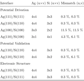
All super-cells in this paper consist of various numbers of Si and Ag unit cells in the plane
of the interface, chosen in order to minimize the effects of lattice mismatch, as illustrated
in figure 1. In all cases the remaining lattice mismatch was accounted for by compression
of the Ag. The compositions and mismatches of all cells used in this paper are presented in
table I.
C. Interatomic potentials
In this section we define the potential models which we have developed for the simulation
on the Si/Ag interface. For Ag we have used an EAM, which has been succesfully employed
for modelling Ag previously36. For Si we used the Tersoff potential model34 which has
also been widely used for the modelling of Si and unlike the EAM can account for bond
directionality as a result of the electronic structure of Si. For the interaction between the Si
FIG. 1. Schematic illustration of the use of super-cells to overcome lattice mismach. Left: Si (u =
7.679 ˚A , v = 7.679 ˚A ) and Ag (u = 5.784 ˚A , v = 5.784 ˚A ) unit cells differ by 25 % in u and v
lattice directions. Right: Si (x3) and Ag (x4) super-cells have no lattice mismatch.
Interface Ag (u×v) Si (u×v) Mismatch (u,v)
Potential Drivation
Ag(111)/Si(111) 4x4 3x3 0.3 %, 0.3 %
Ag(110)/Si(110) 4x4 3x3 0.3 %, 0.3 %
Ag(100)/Si(100) 3x3 2x2 11.5 %, 11.5 %
Ag(110)/Si(100) 3x1 4x1 4.3 %, 6.1 %
Potential Validation
Ag(110)/Si(110) 4x4 3x3 0.3 %, 0.3 %
Ag(110)/Si(110) 4x4 3x2 0.3 %, 6.1 %
Electronic Structure
Ag(110)/Si(110) 4x4 3x3 0.3 %, 0.3 %
Ag(111)/Si(111) 4x4 3x3 0.3 %, 0.3 %
TABLE I. Details of the super-cells used in the three sets of calculations in this paper. In all cases
the number of cells in the u vector direction by the number of cells in the v vector direction of the
[image:7.612.169.441.376.638.2]The Tersoff potential34 is based on a simple pair potential approach. However, the
at-tractive part of the pair potential is modified by a term which depends upon the chemical
environment of the atom, thus effectively taking into account changes in bond hybridization.
The interaction (U(rij)) is calculated as:
U(rij) =fc(rij)[fR(rij)−γijfA(rij)] (1)
wherefR(rij) andfA(rij) are repulsive and attractive terms respectively, fc(rij) is a smooth
cutoff function and γij is the bond-order term, which accounts for the local environment.
The attractive and repulsive terms are calculated using exponential functions, based on the
interatomic separation rij and four parametersAij, aij, Bij, bij
fR(rij) =Aije−aijrij;fA(rij) =Bije−bijrij (2)
The cutoff function ensures a smooth decay of the interaction and is based upon two cutoff
values Rij and Sij
fc(rij) =
1 if rij < Rij, 1
2 + 1 2cos[π
rij−Rij
Sij−Rij] if Rij < rij < Sij,
0 if rij > Sij.
(3)
The bond order term depends upon the angle formed between the two atoms and any
third atom within the cutoff range g(θijk), the cutoff function, two atomic parameters βi
and ηi as well as two additional bi-atomic parametersχij and ωij.
γij =χij(1 +βiηiζ ηi ij)
−1
2ηi, (4)
with
ζij =
X
k6=i,j
fC(rik)ωikg(θijk), (5)
the θ function being defined by three further atomic parameters
g(θijk) = 1 + c2 i d2 i − c 2 i d2
i + (hi−cosθijk)2
. (6)
Furthermore, mixing parameters are defined for interactions between different atomic
types, using the standard mixing rules42
:
aij = (ai+aj)/2, bij = (bi +bj)/2
Aij =
q
AiAj, Bij =
q
BiBj (7)
Rij =
q
RiRj, Sij =
q
The bi-atomic parameters defining the bond order are
χii= 1, χij =χji
ωii= 1, ωij =ωji (9)
In order to ensure that the mixing rules are obeyed, but the Ag atoms do not interact
through the Tersoff potential, we introduce a number of constraints to the parameters used
for the Si-Ag potential. By setting ηAg = 12 and βAg = 0, we ensure that γAg = 1. This
means that by stipulating AAg = BAg and aAg = bAg during the parameter fitting process
we make sure that UAgAg(rij) = 0,∀rij.
In addition to the Tersoff potential interaction between the Si and Ag, we include a short
range electron density term from the Si in the EAM for Ag.
III. RESULTS AND DISCUSSION
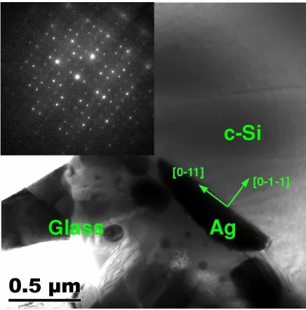
[image:9.612.196.414.403.624.2]A. Experimental Characterization
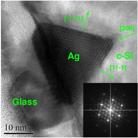
FIG. 2. Bright field TEM image and diffraction pattern of a Ag crystallite (dark contrast area)
embedded in the c-Si matrix (area to the right).
Figure 2 shows images from TEM investigations of the contacting interface region ofthe
FIG. 3. High resolution TEM image of a Ag crystallite (triangular feature) embedded in the c-Si
matrix (area to the right). The inset shows the Fourier transform of the Ag crystallite plus Si
matrix.
silicon (c-Si) surface was textured along the (111) planes prior to Ag deposition. In this image
the dark contrast area highlighted is an Ag crystallite embedded in the c-Si (to the right)
and an amorphous layer (to the left). Such a situation is typical of Ag crystallites in solar
cells. It should be noted that, in general, the fraction of c-Si where Ag crystallite contacts
exist in industrial solar cells is only ∼ 10 %, the majority of the c-Si being in contact with a glass matrix1,37,43,44.
The diffraction pattern inset shows the alignment of the crystals. It reveals that the
two structures are aligned along their (110) planes. Also, the diffraction spots are perfectly
in line, demonstrating that the crystals are aligned to within the accuracy of the TEM. In
addition the diffraction pattern shows that the cells are in a 3 to 4 ratio, which is what would
be expected as this ratio gives almost perfectly matching lattice parameters to minimise
surface strain and corresponds to near-perfect epitaxial growth and.
Similarly figure 3 shows an Ag crystallite; this time the c-Si had a polished (100) surface.
The Ag is once again perfectly aligned with the c-Si; however on this occasion it is the (111)
faces which are in contact with one another. The crystal orientation was determined from the
diffraction pattern (inset), which again shows almost perfect alignment within the accuracy
industrial solar cells45, depending on the surface of the Si onto which the Ag is printed. On
c-Si (100) surfaces the Ag crystallites typically grow in four-sided pyramids with (111)/(111)
Si/Ag interfaces, on c-Si which is textured to reveal the (111) surface three-sided pyramids
with a combination of (110)/(110) and (111)/(111) interfaces are typically found45,46.
B. Fitting the new potential
Due to the scarcity of experimental data available for fitting the Si-Ag interface
poten-tial, we have optimized the parameters to reproduce the results of ab initio simulations.
These include the bond length and binding energy of the SiAg dimer, the geometry
ob-tained after replacing a Ag atom in the unit cell by a Si atom and geometry optimizing, as
well as the geometries and work of separation (wsep) calculated for the Si(111)//Ag(111),
Si(110)//Ag(110), Si(100)//Ag(100) and Si(100)//Ag(110) interfaces. It should be pointed
out that for Si/Ag interface calculations the models employed were not chosen as
represen-titive of the physical reality, but rather as references for forces acting between the species.
Thus the systems were calculated as stacks of Si and Ag with no vacuum gap employed, so
that each unit cell has two interfaces. The work of separation is calculated as47
wsep=
EAgSi−(EAg+ESi)
2A , (10)
in which EAgSi is the relaxed energy of the system with both slabs present, EAg, ESi are
the energies of the individual unrelaxed slabs, A is the interfacial area and the factor of 2 accounts for the presence of 2 interfaces in our model systems.
In addition we have slightly altered the parameters of the Ag EAM36
, in order to reproduce
the energy vs volume results from DFT calculations. This was done as we use the results of
the potential-based calculations to derive structures for DFT simulations of the electronic
properties of the Si-Ag interface.
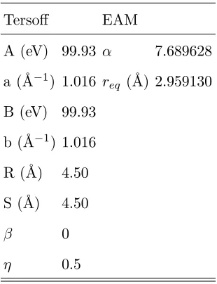
The Tersoff parameters derived for Ag are given in table II, as are the EAM parameters
which have been modified.
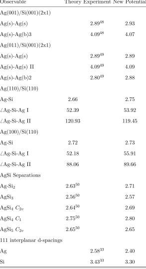
To test the validity of the new potential we have compared to experimental data for the
structure of the Ag(001) interface with the 2x1 reconstructed Si(001) surface, the Ag(011)
interface with the 2x1 reconstructed Si(001) surface48,49 and recent HREM values for the
Tersoff EAM
A (eV) 99.93 α 7.689628
a (˚A−1) 1.016 r
eq (˚A) 2.959130 B (eV) 99.93
b (˚A−1) 1.016
R (˚A) 4.50
S (˚A) 4.50
β 0
[image:12.612.228.383.70.272.2]η 0.5
TABLE II. Potential parameters derived in this work, Tersoff parameters are as in equations 1-7
and EAM parameters are as in36.
level tehoretical calculations; DFT structures of the Ag(110)//Si(110) interface and the
Ag(100)//Si(110) interface (calculated with thicker slabs than used when deriving the
po-tential, see numerical details section), as well as structural details of theoretically calculated
AgSin structures taken from the literature50. The comparisons are presented in table III.
All of our calculated cluster bond lengths are within 5% of the DFT values50, although our
potential was based primarily on condensed state data. Of more interest are the comparisons
to interface structures. The relaxation of the surfaces in contact with one another can be
characterized by the interatomic distances at the surface as well as the inter-layer distances
of the surface to bulk layer atoms. These values are available experimentally for Ag surfaces
in contact with the reconstructed Si(001)(2x1) surface. In all cases the values which we
calculate are within 3 % of the experimental values. When comparing to the DFT structures
of the more realistic interface models we find the interatomic separations obtained from the
potential model to be within 5% of the ab initio results and generally good agreement for
bond angles (see table III). Finally we also compare to recent HREM results for d-spacings
at the Si/Ag interface in a crystalline Si solar cell33, we find that our values are within 0.2
˚
Observable Theory Experiment New Potential
Ag(001)/Si(001)(2x1)
Ag(s)-Ag(s) 2.8948 2.93
Ag(s)-Ag(b)3 4.0948 4.07
Ag(011)/Si(001)(2x1)
Ag(s)-Ag(s) 2.8949 2.89
Ag(s)-Ag(s) II 4.0949 4.09
Ag(s)-Ag(b)2 2.8049 2.88
Ag(110)/Si(110)
Ag-Si 2.66 2.75
6 Ag-Si-Ag I 52.39 53.92
6 Ag-Si-Ag II 120.93 119.45
Ag(100)/Si(110)
Ag-Si 2.72 2.73
6 Ag-Si-Ag I 52.18 55.91
6 Ag-Si-Ag II 88.06 89.66
AgSi Separations
Ag-Si2 2.6350 2.71
AgSi3 2.5650 2.57
AgSi4 C2v 2.6450 2.69
AgSi4 C1 2.7550 2.80
AgSi5 C2v 2.6550 2.65
111 interplanar d-spacings
Ag 2.5833 2.40
[image:13.612.158.451.81.619.2]Si 3.4333 3.30
TABLE III. Comparison of the optimized geometrical properties of SiAg clusters and interfaces
calculated using the new potential and those observed experimentally and calculated from DFT.
C. Interface Structure
We now investigate the geometry and electronic structure of the two interfaces which
have been identified by TEM. The initial step is to use the potential derived in the previous
section to generate a starting geometry for the DFT calculations. The starting geometries
are generated using the Materials Studio51package. The systems are then set up as described
in the numerical calculations section. Using the potential we can investigate a number of
important factors for setting up the DFT calculations. Firstly we can establish a starting
configuration which can be expected to give the lowest energy configuration. This is achieved
in a two step process, by varying the slab separation, followed by the x and y cartesian
co-ordinates of the Ag slab and relaxing the resultant geometry to find the lowest energy
minimum. This required 150 separate geometry optimizations, which would be extremely
time consuming using DFT methods. Secondly we can investigate how far beyond the
interface the geometrical re-arrangements are manifested. This allows us to choose the
smallest possible slabs for the DFT calculation, thus improving efficiency. In the case of both
interfaces it was found that significant re-organization of the atomic positions compared to
the ideal crystal positions (> 0.1 ˚A) occurred only within the first 5 ˚A either side of the
interface.
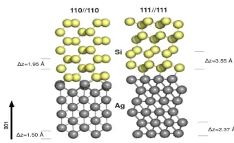
As presented in table IV, the interatomic distance between the Si and Ag surface atoms
is slightly smaller in the 110//110 interface. In the case of the 111//111 interface there
is very little distortion of the surface layer to back layer distances on either side of the
interface, with both Si-Si and Ag-Ag bonds being within 0.01 ˚A of the ideal crystal values.
In the 110//110 case, the Si-Si bond between the surface and back layer is slightly stretched
relative to the perfect crystal, whilst the Ag-Ag bond is slightly compressed. The striking
feature, however, is how little the bond lengths differ between the two interfaces. This
minor difference masks a significant difference between the electronic structures of the two
interfaces as we shall now show.
D. Electronic Structure
Figure 5 shows the charge distribution calculated for the interfacial structures. The
Interface Si-Ag Si-Si Ag-Ag
111 2.69 2.35 2.89
110 2.65 2.36 2.87
TABLE IV. Interatomic separations of Si to Ag and Si (Ag) to first Si (Ag) back layer in ˚A.
to the bulk layers on either side. There is also very little apparent covalent type bonding
between the Si and the Ag. This interface has bonding which is rather metallic in nature,
with a broad charge distribution.
In contrast to this, the 110//110 interface shows substantial charge density interactions
across the interface. The Si-Ag atoms are forming a quasi-covalent bond. The reason for the
major difference in the charge distributions is, we believe, due to the bonding environments
at the different interfaces. At the 111//111 interface the surface Si atoms are back-bonded
to three fully co-ordinted Si atoms. Thus their electronic environment is similar to that in
the bulk crystal. In the 110//110 interface, however, the surface Si atoms are bonded to only
one fully co-ordinated Si and two other interface Si atoms, perhaps resulting in bonds being
formed to Ag. These differences in atomic structure affect the electronic profile of these
interfaces which in turn can have a marked effect on their macroscopic electrical properties
[image:15.612.211.381.482.586.2]as we shall now explore.
FIG. 4. Interface geometries of the 111//111 and 110//110 Si/Ag interfaces, showing inter-layer
spacing along the 001 axis (color online).
Figure 6 shows the valence charge densities averaged in the (001) plane plotted along
the (001) axis in both interfaces. Again this plot makes apparent the difference in electronic
FIG. 5. Charge distribution in the [100] cross-section at the 110//110 (upper) and 111//111 (lower)
Si/Ag interfaces. Charge density contours from 0.001 to 0.281 a.u−3 are shown.
111//111 charge density (figure 6) is that the interlayer spacing along the (001) axis is
greater in this structure (figure 4). Returning to figure 6, at the 110//110 interface there is
a marked decrease in the Ag charge density at the surface layer. There is also a very slight
increase in the charge density at the Si surface layer. This shows an obvious charge transfer
of valence electrons from Ag to Si at this interface. The 111//111 interface shows no such
changes at the interface with the densities on either side being the same as their bulk values.
These analyses reflect the bonding situations revealed in figure 5.
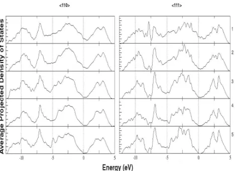
Figure 7 shows the averaged projected density of states (PDOS) for the layers of each
Si slab closest to the Si/Ag interface. It should be noted that the sharper features in the
(111) interface PDOS are most likely due to the fact that there are fewer Si atoms in each
FIG. 6. Averaged, normalized charge densities along the 001 axis of the 110//110 (a) and 111//111
(b) interfaces. The positions of the atomic layers are indicated by a point.
interface we have split each Si layer in the 111//111 (depicted in figure 4) structure into
bilayers, according to their distance from the interface along the (001) axis, for the PDOS
plot.
One of the most important features of the PDOS plots is the existence of states within the
band gap at the surface layer Si atoms. These are the metal-induced gap states (MIGS)7,8.
The MIGS-charge neutrality level (MIGS-CNL) model7, in which the CNL is the energy level
to which the band structure is filled in the neutral system, insists that the presence of these
states seriously affects the Schottky barrier at an interface. As can be seen in the PDOS
plots the MIGS in the 111//111 system decay much more rapidly away from the interface
than those in the 110//110 system. In the 111//111 system the states are almost completely
absent in the second layer of Si atoms, which is less than 1˚A further from the interface than
the first layer. In contrast the 110//110 still displays some MIGS in the second layer of Si
atoms which are 1.95 ˚A further from the interface than the surface layer. We believe that
the reason for the deeper MIGS in the 110//110 system is the presence of electron density
transferred from the Ag layer in the Si layer. As shown in figure 6 this is more prevalent in
FIG. 7. Averaged projected density of states of the Si atoms in each layer moving away from the
Si/Ag interface from the top down. The supercell Fermi level is set to zero.
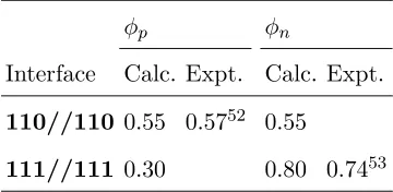
E. Schottky barrier height
A p-type Schottky barrier height (SBH) can be obtained from a supercell calculation as
the difference between the Fermi level of the supercell and the valence-band top (VBT) of
the bulk semiconductor region15,16
. From this the n-type SBH can easily be obtained as the
semiconductor band gap minus the p-type SBH. Of course in these calculations there are no
band-bending effects, due to the absence of dopant and temperature effects. However such
calculations provide insight into SBHs in the ideal limit, and are useful for the comparison
of different interfaces. Whilst MIGS and classic Schottky theories insist that the SBH is
a property only of the bulk materials on either side of the interface, it has been shown
both theoretically and experimentally that the SBH can vary greatly depending on the local
interface structure15–18.
Since, as can be seen in figure 7, the PDOSs of the Si away from the interface still
display some disorder, particularly close to the VBT, we determine the VBT by fitting the
valence band bottom (VBB) of bulk Si to that of the interface system and taking the VBT
from the bulk DOS, as has been done previously15,16
. The n-type SBH is then calculated by
subtracting the p-type SBH from the Si band gap. In this case we use the experimental band
gap, as generalized gradient approximation methods (such as the PBE functional used in
this work) often seriously underestimate band gaps. The SBHs thus calculated are presented
φp φn
Interface Calc. Expt. Calc. Expt.
110//110 0.55 0.5752 0.55
[image:19.612.215.395.72.160.2]111//111 0.30 0.80 0.7453
TABLE V. Schottky barrier heights (φ) for the Si/Ag 110//110 and 111//111 systems as calculated
from supercell simulations.
The SBHs for the two interfaces show a significant difference of 0.25 eV. We propose
that this difference arises from the different bonding structures at the two interfaces. In the
110//110 interface there is a higher degree of covalency between the Si and Ag atoms (figure
5). This, in turn, results in a transfer of some electron density from Ag and Si (figure 6) to
the interfacial region. This charge transfer means that the surface Si sites in the 110//110
system have a slightly less negative charge compared to those in the 111//111 interface.
Within a classical macroscopic model the negative charge in the semiconductor screened
by its dielectric constant is neutralized by a positive charge induced in the metal layer10.
Thus a dipole is established across the interface. This dipole results in the raising of the
electrostatic potential of the semiconductor with respect to the metal. Due to the dependence
of the SBH on the potential difference between the metal and semiconductor10,17,18, this
results in an decreased SBH at the interface. This dipole in the 110//110 interface is lowered
compared to that in the 111//111 interface, due to charge transfer, thus the p-type SBH is
higher in the 110//110 interface.
IV. SUMMARY
We have presented a new potential for the interaction between silicon and silver based
on the Tersoff functional form. The model has been parameterized to fit ab initio data and
validated against both ab initio and experimental data. We have then used this potential
to investigate the geomtery of two Si/Ag interfaces which we have identified, by means of
TEM, in industrially produced solar cells.
The geometries which we have obtained from the potential based calculations have served
calculated SBHs in good agreement with experimental values, showing that the p-type SBH
for the 111//111 Si/Ag interface is significantly lower than that of the 110//110 interface.
This re-inforces the idea that the SBH is dependent not only on the bulk properties of the
materials involved in an interface, but also upon the local structure at the interface.
Using the calculated electronic structure we have attempted to rationalize the difference in
SBH at the two interfaces. We propose that the presence of covalent bonding at the 110//110
interface results in a charge transfer into the interfacial region, leading to a reduction in the
dipole across the interface caused by the negative charge on surface layer Si, which induces
an image charge in the Ag. As this dipole results in the lowering of the p-SBH φp the
reduction of the dipole can explain the higher value of φp at the 110//110 interface.
We believe that, in light of these results, future production of solar cells would benefit
from being tailored to form 110//110 Si/Ag contacts to transport charge generated in n-type
Si, in order to reduce contact resistance. A small contact resistance is particularly desirable
in the n-type Si/Ag contact, due to the fact that this contact is normally formed on the
front side of the solar cell. Meaning that it is desireable to have as small a layer of metal
contact as possible, to allow maximum light penetration into the cell. Thus, a low contact
resistance between Si and Ag is one of the primary concerns when producing solar cells to
ensure good performance of the solar cell despite a small metal/semiconductor contact area.
It should be noted, however, that the barriers calculated here are local barriers for Si/Ag
contacts. The values do not give a global resistance for the entire cell. Whilst the values
give an indication of which interfaces are best for current transport, the incorporation of
the calculated barriers into macroscopic models of the full device will be necessary to fully
appreciate the implications of the results.
ACKNOWLEDGMENTS
The authors acknowledge support from the European Commission grant
MMP3-SL-2009-228513, “Hipersol” as part of the 7th framework package, grant number 228513. In addition
we would like to acknowledge Drs. Jesper Friis, Ole Martin Løvvik and Ulf Ekenberg and
computa-tional resources.
1 C. Ballif, D. M. Hulji´c, G. Willeke, and A. Hessler-Wyser, Appl. Phys. Lett.82, 1878 (2003).
2 Z. G. Li, L. Liang, and L. K. Cheng, J. Appl. Phys.105, 066102 (2009).
3 W. Schottky, Z. Phys.113, 367 (1939).
4 W. Schottky, Z. Phys. 118, 539 (1942).
5 A. Y. C. Yu, Solid-State Elec. 13, 239 (1970).
6 W. Monch, ed., Electronic Structures of Metal-Semiconductor Contacts (Jaca, Milano, 1990).
7 V. Heine, Phys. Rev. 138, A1689 (1965).
8 J. Tersoff, Phys. Rev. Lett. 52, 465 (1984).
9 S. G. Louie, J. R. Chelikowsky, and M. L. Cohen, Phys. Rev. B 15, 2154 (1977).
10 C. Berthod, N. Binggeli, and A. Baldereschi, Phys. Rev. B 68, 085323 (2003).
11 J. R. Waldrop and R. W. Grant, Appl. Phys. Lett.62, 2685 (1993).
12 J. R. Waldrop, J. Appl. Phys.75, 4548 (1994).
13 P. Werner, W. J¨ager, and A. Sch¨uppen, Journal of Applied Physics74, 3846 (1993).
14 J. Hoekstra and M. Kohyama, Phys. Rev. B57, 2334 (1998).
15 M. Kohyama and J. Hoekstra, Phys. Rev. B61, 2672 (2000).
16 S. Tanaka and M. Kohyama, Phys. Rev. B 64, 235308 (2001).
17 Y. F. Dong, S. J. Wang, J. W. Chai, Y. P. Feng, and A. C. H. Huan, Appl. Phys. Lett. 86,
132103 (2005).
18 S. Wang, Y. Dong, C. Huan, Y. Feng, and C. Ong, Mat. Sci. Eng. B 118, 122 (2005).
19 N. Sasaki, S. Watanabe, and M. Tsukada, Phys. Rev. Lett.88, 046106 (2002).
20 Y. G. Ding, C. T. Chan, and K. M. Ho, Phys. Rev. Lett. 67, 1454 (1991).
21 H. M. Zhang and R. I. G. Uhrberg, Phys. Rev. B 74, 195329 (2006).
22 H. Hirayama, T. Komizo, T. Kawata, and K. Takayanagi, Phys. Rev. B 63, 155413 (2001).
23 R. I. G. Uhrberg, H. M. Zhang, T. Balasubramanian, E. Landemark, and H. W. Yeom, Phys.
Rev. B 65, 081305 (2002).
24 H. M. Zhang, J. B. Gustafsson, and L. S. O. Johansson, Phys. Rev. B 74, 201304 (2006).
25 S. J. Chey, L. Huang, and J. H. Weaver, Phys. Rev. B 59, 16033 (1999).
27 F.-C. Chuang, C.-H. Hsu, C.-Z. Wang, and K.-M. Ho, Phys. Rev. B78, 245418 (2008).
28 H. Hong, R. D. Aburano, D.-S. Lin, H. Chen, T.-C. Chiang, P. Zschack, and E. D. Specht,
Phys. Rev. Lett.68, 507 (1992).
29 R. D. Aburano, H. Hong, J. M. Roesler, K. Chung, D.-S. Lin, P. Zschack, H. Chen, and T.-C.
Chiang, Phys. Rev. B52, 1839 (1995).
30 C. Ballif, D. Huijic, A. Hessler-Wyser, and G. Willeke, inPhotovoltaic Specialists Conference,
2002. Conference Record of the Twenty-Ninth IEEE (2002) pp. 360 – 363.
31 Y.-L. Kuo, J.-J. Huang, S.-T. Lin, C. Lee, and W.-H. Lee, Materials Chemistry and Physics
80, 690 (2003).
32 H.-C. Fang, C.-P. Liu, H.-S. Chung, and C.-L. Huang, Microsc. Microanal. 16(2010).
33 M.-I. Jeong, S.-E. Park, D.-H. Kim, J.-S. Lee, Y.-P. Park, K.-S. Ahn, and C.-J. Choi, J.
Electrochem. Soc.157, H934 (2010).
34 J. Tersoff, Phys. Rev. Lett. 56, 632 (1986).
35 J. Tersoff, Phys. Rev. B39, 5566 (1989).
36 X. W. Zhou, H. N. G. Wadley, R. A. Johnson, D. J. Larson, N. Tabat, A. Cerezo, A. K.
Petford-Long, G. D. W. Smith, P. H. Clifton, R. L. Martens, and T. F. Kelly, Acta Mater. 49, 4005
(2001).
37 G. Schubert, Thick Film Metallisation of Crystalline Silicon Solar Cells, Dissertation thesis,
Universitat Konstanz.
38 G. Kresse and J. Furthmuller, Phys. Rev. B 54, 11169 (1996).
39 J. P. Perdew, K. Burke, and M. Ernzerhof, Phys. Rev. Lett. 77, 3865 (1996).
40 G. Kresse and D. Joubert, Phys. Rev. B 59, 1758 (1999).
41 W. Smith and T. R. Forester, J. Mol. Graphics 198/199, 796 (1996).
42 M. P. Allen and D. J. Tildesley, eds.,Computer Simulation of Liquids(Clarendon Press, Oxford,
1987).
43 K.-K. Hong, S.-B. Cho, J. S. You, J.-W. Jeong, S.-M. Bea, and J.-Y. Huh, Solar Energy
Mate-rials and Solar Cells 93, 898 (2009), 17th International Photovoltaic Science and Engineering
Conference.
44 S. Kontermann, M. HÃűrteis, M. Kasemann, A. Grohe, R. Preu, E. Pink, and T. Trupke, Solar
Energy Materials and Solar Cells93, 1630 (2009).
Dissertation thesis, Universitat Konstanz.
46 D. Pysch, A. Mette, A. Filipovic, and S. W. Glunz, Prog. Photovoltaics 17, 101 (2009).
47 M. W. Finnis, J. Phys. : Condens. Mat.8, 5811 (1996).
48 Y. W. Kim, N. G. Park, W. S. Cho, K. H. Chae, C. N. Whang, K. S. Kim, S. S. Kim, and
D. S. Choi, Surface Science 396, 295 (1998).
49 W. S. Cho, J. Y. Kim, N. G. Park, K. H. Chae, Y. W. Kim, S. S. Kim, D. S. Choi, and C. N.
Whang, Surface Science 439, L792 (1999).
50 P.-F. Zhang, J.-G. Han, and Q.-R. Pu, J. Mol. Struc.: THEOCHEM 635, 25 (2003).
51 Materials Studio (Accelrys, Accelrys Software Inc., 2001-2007).
52 J. Garramone, J. Abel, I. Sitnitsky, and V. LaBella, J. Vac. Sci. Technol. A 28, 643 (2010).
![FIG. 5. Charge distribution in the [100] cross-section at the 110//110 (upper) and 111//111 (lower)](https://thumb-us.123doks.com/thumbv2/123dok_us/7994721.206793/16.612.204.406.76.401/fig-charge-distribution-cross-section-upper-lower.webp)