This is a repository copy of
Realization of the welding of individual TiO2 semiconductor
nano-objects using a novel 1D Au80Sn20 nanosolder
.
White Rose Research Online URL for this paper:
http://eprints.whiterose.ac.uk/93841/
Version: Accepted Version
Article:
Qu, K., Zhang, H., Lan, Q. et al. (8 more authors) (2015) Realization of the welding of
individual TiO2 semiconductor nano-objects using a novel 1D Au80Sn20 nanosolder.
Journal of Materials Chemistry C, 3 (43). pp. 11311-11317. ISSN 2050-7526
https://doi.org/10.1039/c5tc01267h
[email protected]
https://eprints.whiterose.ac.uk/
Reuse
Unless indicated otherwise, fulltext items are protected by copyright with all rights reserved. The copyright
exception in section 29 of the Copyright, Designs and Patents Act 1988 allows the making of a single copy
solely for the purpose of non-commercial research or private study within the limits of fair dealing. The
publisher or other rights-holder may allow further reproduction and re-use of this version - refer to the White
Rose Research Online record for this item. Where records identify the publisher as the copyright holder,
users can verify any specific terms of use on the publisher’s website.
Takedown
If you consider content in White Rose Research Online to be in breach of UK law, please notify us by
This is an
Accepted Manuscript
, which has been through the
Royal Society of Chemistry peer review process and has been
accepted for publication.
Accepted Manuscripts
are published online shortly after
acceptance, before technical editing, formatting and proof reading.
Using this free service, authors can make their results available
to the community, in citable form, before we publish the edited
article. We will replace this
Accepted Manuscript
with the edited
and formatted
Advance Article
as soon as it is available.
You can find more information about
Accepted Manuscripts
in the
Information for Authors
.
Please note that technical editing may introduce minor changes
to the text and/or graphics, which may alter content. The journal’s
standard
Terms & Conditions
and the
Ethical guidelines
still
apply. In no event shall the Royal Society of Chemistry be held
responsible for any errors or omissions in this
Accepted Manuscript
or any consequences arising from the use of any information it
contains.
Accepted Manuscript
Journal of
Journal Name
ARTICLE
This journal is © The Royal Society of Chemistry 20xx J. Name., 2013, 00, 1-3 | 1
Please do not adjust margins
Please do not adjust margins
Received 00th January 20xx,Accepted 00th January 20xx
DOI: 10.1039/x0xx00000x
www.rsc.org/
Realization of the Welding of Individual TiO
2Semiconductor
Nanoobjects by Using Novel 1D Au
80Sn
20Nanosolder
Ke Qu,
aHong Zhang,
aQianqian Lan,
aXia Deng,
aXinlong Ma,
aYuanqing Huang,
aJunwei Zhang,
aHongbin Ma,
aBeverley J Inkson,
bDesheng Xue
aand Yong Peng*
aIndividual semiconductor nanowires (NWs) TiO2 were successfully welded together by using novel one-dimensional (1D)
Au80Sn20 (mass ratio) nanosolders at the nano scale for the first time. The nanosolders were electrodeposited into
nanoporous templates to form 1D structure, and their morphology, crystal structure, chemistry and elemental electronic states were systematically characterized. Individual Au80Sn20 nanowires were proved to consist of mixed crystal phases,
including Au5Sn phase with trigonal structure, AuSn phase with hexagonal structure and little SnO2 phase produced by
oxidation of the surface portion. Chemical analysis indicates that the composition is Au80Sn20. The testing of welding
capability either in situ TEM or in situ SEM by nanomanipulators and Infiltration experiment reveal a good wet ability and diffusion ability between the Au80Sn20 nanosolder and TiO2 nanowire. It is believed that our work contribute a special
nanosolders for future nanoscale welding techniques, which also make the bondings of titanium-based semiconductor oxide nanomateirals at the nanoscale a reality.
1. INTRODUCTION
Welding techniques at the nano scale is crucial to the development of nanoscience and nanotechnology because the full utilization of the novel physical and chemical properties of individual nanoobjects is requested to bond them together into nano-electronics, nano-sensors and nano-devices.1-3 Several nanowelding techniques, including thermal heating4 , ion beam deposition5, 6 , laser heating7 , ultrasonic welding8 , electrical welding technique9 , high-energy electron beam irradiation10 , and Joule heating11-13 , has been invented to joint nanoparticles, nanowires, nanobelts, or nanotubes together at the nanoscale so far. For example, the electrical welding technique was used to weld individual Au NWs into nanocircuits and nanopatterns9 . The high-energy electron beam irradiation (EBI) welding technique was used to bond carbon nanotubes together,14 or metallic NWs (Au, Ag, Ni) with a Si NW which forms metal-semiconductor nanojoints.10 However, current nanowelding body materials are dominated to be metallic nanowires and carbon nanotubes. The welding of semiconductor oxide nanoobjects is surprisedly sparse.
Semiconductor oxide nanomaterials have many novel and unique electrical, optical, chemical and biological properties,15 which lead to a great interest for their usage in the fabrication of the next generation nanocircuits, nanotools, nanowires lasers, photon tunneling devices, near-field photo-waveguide
devices, etc.16 Titanium dioxide (TiO2) NWs as one member of
the semiconductor oxide nanomaterial family are considered to have a wide application into photoelectric conversion and energy saving fields based on their optical, photocatalytic, photohydrophilic properties.17, 18 Bonding individual TiO2
nano-objects together or with electrode pads to form secure, functional and long-lasting nanoscale systems is significant and urgent for the quick realisation of their practical applications. There are two attempts on the welding of TiO2 NWs onto
electrode pads.19, 20 But, individual TiO2 NWs have not been welded together so far as far as we know. It is believed to be due to the high melting point and good chemical stability of TiO2, which is not conductive to bond them together directly.
Alike traditional welding method, using a proper solder media to bond the TiO2 nanoobjects should be an effective way,
which also have the opportunity to specifically tailor the weld properties of these joints such as chemistry, strength, and conductivity.
Many studies have shown that there exists good diffusion between titanium and gold.21, 22 In the previous report,22 Ti was verified to sufficiently diffuse through 260 nm Au thin film at temperatures ranging between 200 and 400 , and the surfacial oxidation of Ti can enhance the diffusion. Therefore, it is feasible to utilize gold-rich nanosolders with a moderate melting point to weld titanium-based semiconductor nanometarils at the nano scale. It is worthy to note that the electronic industry banned the lead to use as an elemental composition of solders on 1 July 2006 due to its high toxicity and environmental pollution. The exploitation and studies of Au-Sn solders become more important and necessary, especially, when the nanoscale welding techniques have turned into practical ways to connect nanoscale building
Page 1 of 7
Journal of Materials Chemistry C
Journal
of
Materials
Chemistry
C
Accepted
COMMUNICATION
Journal Name
blocks in the future nano industry. Au80Sn20 alloy solder
composed of 80 wt% gold and 20 wt% tin could be a good candidate, which is at the eutectic point with a relatively low melting point of 278 on Au-Sn binary phase diagram. As an important industrial solder, Au80Sn20 solder is typically used in
the welding of opto/microelectronic packaging areas,23 and semiconductor materials. In comparison with the conventional solders, Au80Sn20 solder has many excellent properties, such as
high strength, good corrosion resistance, high thermal conductivity, good electrical properties, free-flux, and so on, which make it an ideal solder.24-27 However, nanoscale Au80Sn20 alloy and its application into individual nanoscale
building blocks of semiconductor or other materials in nano space have not been reported so far.
In this work, we present a preparation of 1D Au80Sn20 alloy
nanosolders by using electrodeposition into nanoporous templates. The morphological, structural and chemical characterizations of 1D Au80Sn20 alloy nanosolders have been
systemically investigated. Furthermore, the Au80Sn20
nanosolders have been used to weld individual TiO2 NWs
together. It is believed that our work not only contributes an important nanosolder for the nanowelding techniques, but also takes the first step to realize the welding of semiconductor oxide nanomaterials, which is critical and significant for the transformation of semiconductor nanomaterials into electronics, sensors or nano-devices.
2. EXPERIMENTAL SECTION
2.1. Preparation of 1D Au80Sn20 alloy nanosolders.
1D Au80Sn20 alloy nanosolders were prepared by DC electrodeposition into anodic aluminum oxide (AAO) templates or polycarbonate (PC, Anodisc, Whatman Inc., Florham Park, NJ, USA) templates with 50 nm diameter pores. The AAO templates were prepared in-house, of which detailed procedures were described in our previous report.28, 29 One side of the non-barrier-layered AAO/PC templates was sputtered by thermally evaporating a 50 nm Ag thin film, serving as the working electrode. The electrodeposition was achieved in a three-electrode electrolytic cell at room temperature on a CHI630B electrochemical workstation, in which the reference electrode was a saturated calomel electrode (SCE) and the counter-electrode was a graphite sheet. The electrodeposition electrolyte is composed of 0.016 M HAuCl4•4H2O, 0.007 M SnCl2•2H2O, 0.125 M ammonium
citrate, 0.059 M Na2SO3 and 0.01 M L-ascorbic acid.
HAuCl4•4H2O and SnCl2•2H2O are the main salts to provide
Au3+ and Sn2+. Na2SO3 is a complexing agent for Au 3+
. Ammonium citrate is a complexing agent for Sn2+, and also an auxiliary complexing agent for Au3+. L-ascorbic acid is an antioxidant. The pH value of the electrodeposition electrolyte was 5.5-6.0. Voltammetric experiments were completed to determine the optimal electrodeposition potentials for the co-electrodeposition AuSn alloy. In this work, a -1.4 V potential is applied to obtain Au80Sn20 eutectic alloy nanosolders, of which
typical curve of the time dependence of the observed current
during the growth of AuSn alloy nanowires in AAO/PC templates is shown in Fig. S1. The chemical composition of AuSn alloy nanosolders is strongly dependent on electrodeposition potential. According to XPS analysis, a -1.3 V potential obtained a Au50Sn50 composition. The typical
deposition time for PC templates is set up to 30 mins, and for AAO templates is 120 mins, which determine the length of nanowires (Fig. S2). The electrodeposition electrolyte was continuously agitated throughout by a magnetic stirrer.
2.2. Fabrication of TiO2 nanowires.
TiO2 nanofibers were fabricated by using a conventional
electrospinning method. In a typical synthesis, 1.2 ml tetrabutyl titanate was mixed with 2.2 ml acetic acid and 1.6 ml ethanol. After 10 min, 3.6 ml ethanol and 0.4 g PVP (Aldrich, Mw 1 300 000) were added, followed by magnetic stirring for about 1 h (with the solution held in a capped bottle). The mixture was immediately loaded into a plastic syringe equipped for electrospinning. The electrospinning process was performed by a dedicated electrospinning facility at 18 kV DC voltage, 15 cm spacing between needle tip and collector, and a feed rate was fixed with 0.4 ml/h. The electrospun polymer composite fibers were collected using alumina crucibles and then calcined at 500 for 2 h with a heating rate of 1 /min in air. The sample was finally allowed to cool to room temperature.
2.3. Characterization.
The morphological, crystal structural and chemical characterisation of the 1D Au80Sn20 nanosolder were analyzed
on a nano-scale using field emission scanning electron microscopy (FESEM, Tescan Mira 3 xmu, Czech Republic), high-resolution transmission electron microscope (HRTEM, TecnaiTM G2 F30, FEI, US) equipped with energy-dispersive X-Ray analysis (EDAX, AMETEK Co., LTD), high angle annular dark field and scanning transmission electron microscopy (HAADF-STEM), X-ray photoelectron spectroscopy (XPS, Kratos Axis Ultra DLD, Japan). The AAO templates or PC templates were completely dissolved in 0.1 M sodium hydroxide solution or dichloromethane for releasing nanowires, which are then rinsed with distilled water and dispersed on holey carbon coated copper grids for TEM, STEM, EDX and analysis.
2.4. Welding of TiO2 nanowires in situ TEM and in situ SEM by
nanomanipulators.
The testing of welding capability of 1D Au80Sn20 nanosolder into TiO2 semiconductor oxide nanowires at the nanoscale space were carried out in-situ the HRTEM operated at 300 kV and spot size 1. Individual TiO2 nanowires and Au80Sn20
nanosolders were successively dispersed on holey carbon coated Cu grids to obtain cross-sectioned structures.
A similar quality test was also carried out by using four nanomanipulators (Kleindiek Nanotechnik, Germany) equipped with nichrome nanotips and a Keithley 6487
picoammeter in situ SEM to weld TiO2 nanopatterns at the
Journal
Journal NameCOMMUNICATION
This journal is © The Royal Society of Chemistry 20xx J. Name., 2013, 00, 1-3 | 3
Please do not adjust margins
Please do not adjust margins
nanoscale. The data acquisition and nanowelding signal were automated using a dedicated multifunctional program.
2.5. Infiltration experiment.
The nanowire solder infiltration experiments were carried out in a programmable high-temperature tube furnace. The solder nanowires were dropped onto TiO2 substrate and SiO2
substrate. TiO2 substrate was fabricated by a spin-coating
method30 and SiO2 substrate was obtained commercially. Nitrogen purging was used to avoid a further oxidation of nanosolders during this process. The temperature was firstly increased to approximate 200 ~ 220 for 5 min to preheat the wires, then briefly raised to 320 for 30 min to ensure a complete melt and diffusion. The TiO2/SiO2 substrates were
cooled down to room temperature and then brought out of the furnace. The detection of infiltration effect was assisted by two in situ SEM nanomanipulators (Kleindiek Nanotechnik, Germany) equipped with nichrome nanoprobes/nanotips.
3. Results and Discussion
3.1. Morphologies, crystal structural and chemical characterization of individual 1D Au80Sn20 nanosolders.
Fig. 1a shows a representative HAADF-STEM image of a bundle of 1D Au80Sn20 nanosolders prepared by polycarbonate (PC)
template, of which PC template has been completely dissolved. Individual Au80Sn20 nanowires have uneven
diameter, alike cylinders, which are replica of the channels of PC templates. The size statistics reveals that the top diameter is approximately 50 nm and the bottom diameter is approximately 120 nm. The average length for the most of nanowires is around 3 µm. The 1D Au80Sn20 nanowires
prepared by AAO template are seen in Fig. 1b, showing a continuous structure with uniform size and large aspect ratio, alike hairs. The size statistics reveals that the average diameter of the prepared Au80Sn20 nanowires is approximately 50 nm.
The average length for the most of nanowires is about 5 µm. The crystalline structures of individual 1D Au80Sn20
nanosolders are characterized in detail using selected-area electron diffraction (SAED) and high-resolution TEM (HRTEM). The large magnified TEM image as shown in Fig. 1c displays that individual Au80Sn20 nanowires consist of many crystal
grains stacking along the nanowire axis, and the surface is slightly oxidized (about 3~4 nm thickness, as marked by red double lines). Its corresponding SAED pattern is shown in Fig. 1d, revealing that the individual 1D Au80Sn20 nanosolders is
multi-crystal. The rings can be well indexed to two sets of lattice planes. The yellow one can be well indexed to the (110), (006), (116), (300) and (223) planes of the trigonal Au5Sn phase. The red one can be well indexed to the (102), (210), (212), (114) and (205) planes of the hexagonal AuSn phase. Fig. 1e and 1f show lattice-resolution images of the Au5Sn phase and AuSn phase marked by white squares E and F in Fig. 1c. The interplanar distances are measured to be 2.247 Å and 2.546 Å for Au5Sn phase in Fig. 1e, matching with (113) and (110) planes of the trigonal Au5Sn phase. The interplanar
distances are measured to be 1.773 Å and 2.222 Å for AuSn phase in Fig. 1f, matching with(201) and (102) planes of the hexagonal AuSn phase. The corresponding FFT patterns and crystal structure simulation of the areas ‘E’ and ‘F’ are shown in the insets of Fig. 1e and 1f. The crystal structure was further investigated by XRD technique. Figure S3 shows a typical XRD spectrum of 1D Au80Sn20 nanosolders embedded into PC templates with a 100 nm Cu thin film evaporated as the working electrode, which also shows a mixture of trigonal Au5Sn crystal phase and hexagonal AuSn crystal phase. It is then concluded that the as-deposited 1D Au80Sn20 nanosolder is comprised of trigonal Au5Sn phase and hexagonal AuSn phase, which preserve their bulk crystal structure.24
Fig. 1. (a) HAADF-STEM image of 1D Au80Sn20 nanosolders dissolved from PC template. (b) TEM image of single 1D Au80Sn20 nanosolder fabricated by AAO template. (c) The large
magnified TEM image of individual 1D Au80Sn20 nanosolders. (d) SEAD image of individual 1D Au80Sn20 nanosolders. Yellow
for Au5Sn phase and red for AuSn phase. (e) and (f) Lattice-resolution HRTEM image of Au5Sn phase and AuSn phase form the white squares in (c). Insets, the corresponding FFT patterns and crystal structure simulation.
The chemical composition of individual Au80Sn20 alloy
nanosolder is analyzed by EDX spectrum (in Fig. 2a), of which detected area come from the region A marked by blue circle in Fig. 1a. The Au and Sn peaks come from the 1D Au80Sn20 alloy
nanosolders. The O peak originates from the thin oxide layer covered on the surfaces of the 1D nanosolders as observed in Fig. 1c, which is deduced to their exposure in the air after released from the templates. The C and Cu peaks are believed to derive from the holey carbon coated copper grid, which was confirmed by the measurement of an EDX baseline of an empty holey carbon coated copper grid. Quantitative analysis of this spectrum reveals that the chemical composition of individual 1D Au80Sn20 nanosolders is a 80.1:19.9 weight ratio
of Au:Sn, referring a Au80Sn20 chemical phase. The chemical
elemental distributions of 1D Au80Sn20 nanosolders were further studied by EDX elemental mapping analysis techniques (Fig. 2b-d). Fig. 2b shows a representative HADDF-STEM image of two 1D Au80Sn20 nanosolders. Fig. 2c and 2d display the EDX
elemental mappings of Au-Lα (9.71 keV) and Sn-Lα (3.44 keV), respectively. The elements of Au and Sn are evenly distributed
Page 3 of 7
Journal of Materials Chemistry C
Journal
of
Materials
Chemistry
C
Accepted
[image:5.612.315.542.209.359.2]COMMUNICATION
Journal Name
throughout the whole nanosolder, indicating a uniform Au80Sn20 chemical phase.
Fig. 2. Chemical analysis of the 1D Au80Sn20 nanosolders: (a)
EDX spectrum of a bundle of 1D Au80Sn20 nanosolders from Fig. 1a as marked by blue circle. (b) HAADF-STEM image. (c) Au elemental mapping. (d) Sn elemental mapping. (e) XPS spectra of Au 4f and Sn 3d after the specimen was sputtered by Ar ion for 0, 30, 60, 100, 140, 190 and 240 s, respectively. Pink for 0 s, purple for 30 s, blue for 60 s, green for 100 s, yellow for 140 s, orange for 190 s, red for 240 s.
In order to accurately determine the electronic states, the as-grown 1D Au80Sn20 nanosolders were further examined by
XPS while they were still in situ embedded in the PC templates. The Ar ion beam sputtering was employed to realize the analysis of layer by layer. The templates were cross-sectioned from the top surface of the PC template, which was parallel to the 1D Au80Sn20 nanosolder length axes. Fig. 2e shows the relevant XPS spectra of Au 4f and Sn 3d after Ar ion beam sputtering for 0 s, 30 s, 60 s, 100 s, 140 s, 190 s and 240 s, respectively. The binding energies were calibrated by using the C 1s peak of 285 eV as a standard. It is seen that the Au 4f 7/2 peaking at 84.0 eV bonding energy in Fig. 2e can be attributed to AuSn (binding energy is 84.20 eV) or Au5Sn (binding energy is 84.14 eV), but it can not be distinguished from XPS because its resolution is about 0.3 eV. There is no peak shift before and after Ar ion beam sputtering, indicating a stability of Au chemical phase along with nanowire length. The Sn 3d 5/2 spectra consist of two peaks located at 484.3 eV and 486.4 eV (marked by two double white lines), indicating a formation of metallic Sn and SnOx respectively. This result indicates that the top ends of the 1D Au80Sn20 alloy solders which are exposed to air have been partly oxidized. After sputtering 240 s, the quantitative analysis of XPS wide spectrum reveals that the 1D Au80Sn20 nanosolders reach a stable 80.17:19.83 mass ratio of
Au:Sn, and have not been detected any oxygen peak. Therefore, the chemical composition of the 1D Au80Sn20
nanosolders in this work is inferred to be Au80Sn20.
3.2. Welding individual TiO2 nanowires together by using 1D
Au80Sn20 nanosolders in situ TEM.
Fig. 3. (a-d) The welding process of two individual TiO2
nanowires by using Au80Sn20 nanosolders in HRTEM. Bar = 0.2
µm. (e-h) EDX elemental mappings of Au-Lα (9.71 keV), Sn-Lα (3.44 keV), Ti-Kα (4.51 keV) and O-Kα (0.52 keV). Inset, the HADDF-STEM image of welded area.
Individual 1D Au80Sn20 nanosolders have been used in the application of welding nanopatterns at the nanoscale to test their quality as nanosolder. Fig. 3 shows the whole process of welding two TiO2 nanowires together by using four 1D
Au80Sn20 nanosolders via a high-energy electron beam irradiation nanowelding technique in situ HRTEM. The crossed structure (Fig. 3a) was achieved by successively dispersing the electrospun TiO2 nanowires (see supplementary Fig. S4 for their structural and chemical characterization) and the 1D Au80Sn20 nanosolders on the holey carbon coated Cu grids.
After the electron beam irradiated, the 1D Au80Sn20
nanosolders gradually melted (Fig. 3b), diffused into TiO2
nanowires (Fig. 3c) and eventually welded the two TiO2
nanowires together (Fig. 3d). The TiO2 nanowires always
remained their morphologies and structure during the whole welding process, which is due to their high melting point (the melting point of bulk TiO2 is approximately 1800 ). However, Fig. 3d only intuitively displays a connection of the two TiO2
nanowires. Solid evidence is required.
Fig. 4. Diagrams of the diffusion of Ti into Au80Sn20 nanosolder by grain boundaries diffusion mechanisms.
EDX elemental mapping technique was employed to check
the quality of nanoweld. The inset of Fig. 3e shows a HADDF-
Journal
of
Materials
Chemistry
C
Accepted
[image:6.612.69.298.82.303.2] [image:6.612.313.545.88.218.2] [image:6.612.315.543.504.651.2]Journal NameCOMMUNICATION
This journal is © The Royal Society of Chemistry 20xx J. Name., 2013, 00, 1-3 | 5
Please do not adjust margins
Please do not adjust margins
STEM image of the welded junction, where the large white spot indicates a rich accumulation of gold and uniform chemical phase. Fig. 3e to 3h show the corresponding EDX elemental mappings of Au-Lα (9.71 keV), Sn-Lα (3.44 keV), Ti-Kα (4.51 keV) and O-Ti-Kα (0.52 keV), respectively. The elements of Au and Sn are evenly distributed throughout the welded junction, indicating the even Au80Sn20 chemical phase preserves after the welding and consistent with the HADDF-STEM observation. The elements of Ti and oxygen are also distributed throughout the welded junction. As the Sn is easy to be oxidized, it is deduced that the oxygen element of the welded junction mainly comes from the tin oxidization during the welding process. The Ti mapping reveals that the Ti element has diffused into the nanosolder residue after the welding of electron beam irradiation. Grain boundaries diffusion mechanism31, 32 is speculated to cause the Ti diffusion into the Au80Sn20 nanosolder residue. As measured by above
HRTEM and SEAD in Fig. 1c-1f, the individual 1D Au80Sn20 nanosolders is polycrystal, which is beneficial to the diffusion of Ti atoms into the grain boundaries of Au-based alloys according to the previous reports.23 During the irradiation of electron beam, the Ti atoms diffused from the surface of TiO2
nanowires into the grain boundaries of Au80Sn20 nanosolder.
Then Ti atoms eventually left it and continued their diffusion in the lattice regions adjacent to the boundary, which thus gave rise to a volume diffusion zone around the boundary. Fig. 4 principally illustrates the schematic diagrams of the diffusion process. The continuous distribution of Ti element ranging from the welding bodies TiO2 nanowires to the welded
junction indicates a formation of integrally reliable bonding, showing that the welded junction should be electrically conductive and mechanically strong. This result also proves that the prepared Au80Sn20 nanosolder in this work should be
suitable in the applications of welding other titanium-based nanomaterials.
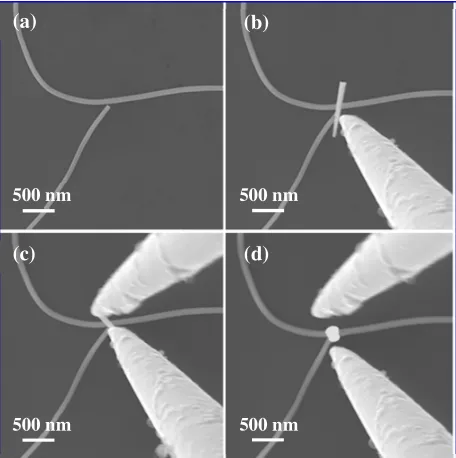
Fig. 5. Nanowelding two 110 nm TiO2 nanowires using a
sacrificial 1D Au80Sn20 nanosolder by nanomanipulators in situ
SEM. (a) Assembly of a " " nanopattern; (b) Placement of the sacrificial 1D nanosolder in contact with the nanostructure to be welded; (c) Preweld softening of the 1D nanosolder and contact to the two nanowires to be welded; (d) Nanowelding the nanowires together by a rectangular voltage pulse through the solder nanowire, causing significant material diffusion onto the junction.
The welding test was also performed by nanomanipulators in situ SEM. Figure 5 illustrates the whole proccess, which is the same as our previous reports.9, 29 Two TiO2 nanowires with
110 nm diameter were mechanically manipulated and assembled into a simple nano-pattern like Chinese word on a SiO2 (100nm)/Si wafer (Fig. 5a), and then a sacrificial 1D
Au80Sn20 nanosolder with 130 nm diameter and 1.3 um length
used as nanosolder was placed onto the assembled nanopattern at the weld point as shown in Figure 5b. Prior to welding, a moderate current (about 80% maximum current density of a single 130 nm 1D Au80Sn20 nanosolder) was
applied to soften the Au80Sn20 nanosolder for 1 ∼ 2 minutes,
which was for inducing the first join to the pattern (Fig. 5c). The softening of the sacrificial nanosolder is due to Joule-heating and can greatly improve the controllability and reliability of the nanowelding procedure. A linear pulse signal of 1.5 V and 300 ms width was then run through the solder to form the weld utterly. The short voltage pulse causes significant Joule heating and associated rapid material diffusion of the 1D nanosolder onto the chosen junction (Figure 5d). During the whole welding process, the 1D Au80Sn20
nanosolder showed a good mechanical strength, controllability, reliability and wettability with the TiO2 semiconductor
nanowires. The mechanical strength of the Au80Sn20 solder
nanojoint was strong enough to enable welded structures to be directly lifted up by a SEM nanomanipulator. This result further proves that the 1D Au80Sn20 nanosolder is a reliable
(a)
(b)
(c)
(d)
500 nm
500 nm
500 nm
500 nm
Page 5 of 7
Journal of Materials Chemistry C
Journal
of
Materials
Chemistry
C
Accepted
[image:7.612.313.541.62.291.2]COMMUNICATION
Journal Name
and high performance nanosolder material for welding titanium-based materials in the nanoscale space.
3.3. Infiltration experiment.
Infiltration experiment was further carried out to verify the solderability between TiO2 nanowires and Au80Sn20
nanosolders. Fig. 6 shows the SEM images of individual 1D Au80Sn20 nanosolders after sintered by a tube furnace on TiO2
substrate and SiO2 substrate, revealing that the wire-shaped Au80Sn20 nanosolders have been melted into spherical particles
(about 1 µm in diameter). The choice of SiO2 substrate is only
for a comparison. In order to observe the internal bonding features between the nanosolder particles and substrates, in-situ SEM nanomanipulators equipped with nichrome nanoprobes/nanotips were used to mechanically push away the formed nanosolder particles (Fig. 6a and 6d), which reveals whether there is inter-diffusion between the nanosolder and substrates. The contact angle was obtained by rotating sample stage to 90°, as shown in Fig. 6c and 6f. In the case of TiO2
substrate, it is seen that the contact angle is smaller than 90°, revealing that the Au80Sn20 nanosolders well spread on the surface of TiO2 substrate. This result proves that the Au80Sn20
nanosolders can infiltrate with TiO2. In addition, it is also seen
that the contrast of left mark is quite bright, revealing a large amount of Au80Sn20 nanosolder residue left. This result
indicates that a solid connection between the TiO2 and
Au80Sn20 nanosolder was formed, which is consistent with
above welding experiment as shown in Fig. 3 and Fig. 5.
Fig. 6. The result of infiltration experiment for Au80Sn20
nanosolders with TiO2 and SiO2 substrates: (a) Nanoprobe
approaching the sintered nanosolder on TiO2 substrate. (b) The bonding trace left after the nanosolder was pushed away by the nanoprobe on TiO2 substrate. (c) The lateral profile of a
melted nanosolder on TiO2 substrate. (d) Nanoprobe
approaching the sintered nanosolder on SiO2 substrate. (e) The non-bonding trace left after the nanosolder was pushed away by the nanoprobe on SiO2 substrate. (f) The lateral profile of a
melted nanosolder on SiO2 substrate.
In comparison with the case of SiO2 substrate (Fig. 6d - 6f),
an opposite result is observed. After the melted Au80Sn20
nanosolder particle on the SiO2 substrate was pushed away by
the nichrome nanoprobe (Fig. 6e), the left trace is hard to be
observed (the original position marked by red arrow). From Fig. 6f, it is seen that the contact angle is bigger than 90° and the Au80Sn20 nanosolders do not infiltrate with SiO2. That is, SiO2 is
not solderable by the Au80Sn20 nanosolders. The result was
also verified by the welding of SiO2 nanowires using 1D
Au80Sn20 nanosolders in TEM as shown in Fig. S5. In addition, it is also seen in Fig. 6d and 6f that the melted Au80Sn20
nanosolder has an ideal spherical shape, revealing that the surfacial oxidization of individual 1D Au80Sn20 nanosolders as
observed above (Fig. 1c) nearly does not influence their solderability and wettability. The comparative infiltration experiments further prove that the 1D Au80Sn20 nanosolders
have a good solderability and wettability to TiO2
semiconductor.
4. Conclusions
In summary, we have demonstrated a fabrication of 1D Au80Sn20 nanosolders and applied them into the welding of
individual TiO2 semiconductor nanowires at the nano scale for
the first time. The analysis of crystal structures prove that the individual Au80Sn20 alloy nanosolders contain two eutectic
phases, including Au5Sn and AuSn phases. Chemical analysis confirm that the mass ratio of Au:Sn is 80:20. The experimental results also reveal that the Ti element has diffused into the nanosolder residue during the welding of electron beam irradiation, which is further confirmed by the infiltration experiments. The good solderability and wettability between the 1D Au80Sn20 nanosolders and TiO2 materials
indicate that the Au80Sn20 nanosolder should be also suitable in
the applications of welding other titanium-based nanomaterials. Our work is believed to contribute a special nanosolder for future nanoindustry, which can realize the bonding of tin-based semiconductor oxide nanomateirals at the nanoscale.
Acknowledgements
This work is supported by National Basic Research Program of China (2012CB933104), National Natural Science Foundation of China (11274145 and 51571104), MOST International Cooperation Funds (2014DFA91340), Program for Changjiang Scholars and Innovative Research Team in University (Grant No. IRT1251), and the Fundamental Research Funds for the Central Universities (lzujbky-2013-19, and 2022013zrct01).
Notes and references
1 A. Figuerola, I. R. Franchini, A. Fiore, R. Mastria, A. Falqui, G. Bertoni, S. Bals, G. V. Tendeloo, S. Kudera, R. Cingolani and L. Manna, Adv. Mater., 2009, 21, 550-554.
2 Y. N. Xia, P. D. Yang, Y. G. Sun, Y. Y. Wu, B. Mayers, B. Gates, Y. D. Yin, F. Kim and Y. Q. Yan, Adv. Mater., 2003, 15, 353-389. 3 S. Han, S. Hong, J. Ham, J. Yeo, J. Lee, B. Kang, P. Lee, J. Kwon,
S. S. Lee, M. Y. Yang and S. H. Ko, Adv. Mater., 2014, 26, 5808-5814.
4 Y. Wu and P. Yang, Adv. Mater., 2001, 13, 520-523.
Journal
of
Materials
Chemistry
C
Accepted
[image:8.612.68.296.383.534.2]Journal NameCOMMUNICATION
This journal is © The Royal Society of Chemistry 20xx J. Name., 2013, 00, 1-3 | 7
Please do not adjust margins
Please do not adjust margins
5 Z. Wang, L. Yu, W. Zhang, Y. Ding, Y. Li, J. Han, Z. Zhu, H. Xu, G. He, Y. Chen and G. Hu, Phys. Lett. A, 2004, 324(4), 321-325. 6 V. Gopal, V. R. Radmilovic, C. Daraio, S. Jin, P. Yang and E. A.
Stach, Nano Lett., 2004, 4(11), 2059-2063.
7 J. K. Seol and J. D. Jeon, App. Phys. Lett., 2005, 86 (3), 033112. 8 C. Chen, L. Yan, E. Kong and Y. Zhang, Nanotechnology, 2006,
17, 2192-2197.
9 Y. Peng, A. G. Cullis and B. J. Inkson, Nano Lett., 2009, 9, 91-96.
10 S. Xu, M. Tian, J. Wang, J. Xu, J. M. Redwing and M. H. W. Chan, Small, 2005, 1(12), 1221-1229.
11 H. Tohmyoh, T. Imaizumi, H. Hayashi and M. Saka, Scripta Mater., 2007, 57(10), 953-956.
12 H. Tohmyoh, J. Appl. Phys., 2009, 105, 014907.
13 H. Hirayama, Y. Kawamoto, Y. Ohshima and K. Takayanagi,
Appl. Phys. Lett., 2001, 79(8), 1169-1171.
14 D. N. Madsen, K. Mølhave, R. Mateiu, A. M. Rasmussen, M. Brorson, C. J. H. Jacobsen and P. Bøggild, Nano Lett., 2003, 3, 47-49.
15 J. H. Ahn, H. S. Kim, K. J. Lee, S. Jeon, S. J. Kang, Y. G. Sun, R. G. Nuzzo and J. A. Rogers, Science, 2006, 314, 1745-1757. 16 L. D. Zhang and X. S. Fang, J. Nanosci. Nanotechnol. 2008,
8(1), 149-201.
17 P. Ravirajan, D. D. C. Bradley, J. Nelson, S. A. Haque, J. R. Durrant, H. J. P. Smit and J. M. Kroon, Appl. Phys.Lett., 2005, 86, 143101.
18 A. Kitiyanan and S. Yoshikawa, Mater. Lett., 2005, 59, 4038-4040.
19 R. H. Wang, C. M. Ruan, D. Kanayeva, K. Lassiter and Y. B. Li,
Nano Lett., 2008, 8, 2625-2631. 20 Z. Jin, patent, CN 201310571335, 2014.
21 J. M. Poate, P. A. Turner and W. J. DeBonte, J. Appl. Phys., 1975, 46, 4275-4283.
22 E. M. William, G. Giuliano and M. Thomas, Thin Solid Films, 2010, 518, 2585-2591.
23 D. Kim and C. C. Lee, Mater. Sci. Eng. A, 2005, 416, 74-79. 24 V. Chidambaram, J. Hattel and J. Hald, Mater. Des., 2010, 31,
4638.
25 J. H. Kuang, M. T. Sheen, C. H. Chang, C. C. Chen, G. L. Wang and W. H. Cheng, IEEE Trans. Adv. Packag., 2001, 24, 563. 26 G. Elger, M. Hutter, H. Oppermann, R. Aschenbrenner, H.
Reichl and E. Jager, Microsyst. Technol., 2002, 7, 239.
27 J. W. R. Tew, X. Q. Shi and S. Yuan, Mater. Lett., 2004, 58, 2695.
28 Y. Peng, H. L. Zhang, S. L. Pan and H. L. Li, J. Appl. Phys., 2000, 87, 7405.
29 H. Zhang, J. W. Zhang, Q. Q. Lan, H. B. Ma, K. Qu, B. J. Inkson, N. J. Mellors, D. S. Xue and Y. Peng, Nanotechnology, 2014, 25, 425301.
30 X. D. Li, C. T. Gao, H. G. Duan, B. A. L, X. J. Pan and E. Q. Xie,
Nano Energy, 2012, 1, 640-645.
31 A. E. Austin and N. A. Richard, J. Appl. Phys. 1961, 32, 1462-1471.
32 C. Herzig and S. V. Divinski, Mater. Trans., 2003, 44, 14-27.