...
DIISCIIII'T'IOIf DAta...
" . " , .A PROD. RELEASE ECO #0621 \',.\'" -~ ~ , . . . -.~
B9 REV ROLL PER ECO #0656A '.-:" -~i ~
Ba REV ROLL PER ECO #0686 \-;~::.~~ ~
Bb REV ROLL PER ECO #0780 8-\1'~1
~
.--" ". '--'-"
Be REV ROLL PER ECO #0968
4-(o'RB
D~
,-)
r !
"
'''-CODE IDENT
CONT" NO.AR.m
OR
BY
CHK BY FUNCTIONAL SPEC. CPU-32 MC68020
REVIEW A PPLICA TION PROCESSOR
ENGINEER
A
DWG.NO.
FS-02234-02REV
&:..,
Arete Systems
Corporation
1100 and
1200
CPU-32 MC68020 Application Processor
Functional Specifications
Restricted Use Document. Possession of this document does not convey any
legal rights to the holder. No form of use of this document is allowed
without prior consent of Arete Systems Corporation.
Functional Specifications
CPU32 - MC68020 Application Processor Board
TABLE OF CONTENTS
Section 1. Introduction
MC68020 Microprocessor ...•...•...•... 1-1
MC68000 Compatibility ... 1-1
Cache Memory ... 1-1
Diagnostics ... 1-1
Memory Management ... 1-2
Configurations ... 1-2
CPU-32 Block Diagram ... 1-2
Section 2. Functional Characteristics
Performance ... 2-1
Specifications ... 2-1
Section 3. Theory of Operation
Architecture ... 3-1
Motorola MC68020 32-Bit Microprocessor ... 3-1
Motorola MC68881 Math Processor ... 3-1
CPU-32 Functional Elements ... 3-1
'Primary Map ... 3-1
Secondary Map ... 3-1
Physical Page Number ... 3-1
Page Attributes ... 3-2
Process 10 ... 3-2 Code Page Attribute ... 3-2
Cacheable Attribute ... 3-2
Written Statistic ... 3-2
Accessed Statistic ... 3-2
Write Protect Attribute ... 3-2
Cache Memory ... 3-2
[image:3.618.70.553.420.697.2]gPU-92
Functional Specifications
Updater .•..•...•.•••..•.•.•••••.•...••...••....•...••.••••••..••.••••••..•••.•••••...•..•.••.••••...•••••••.••.••••••.•..•....•••..•.•....•... 3-2
CPU-32 Master Operation ...•.•...•...•....•...•.•....•..•...•...••...•...•... 3-2
CPU-32 Slave Operation •...•...•.•...•.•.•...••.•.•.••.•.••.•••..•...••...•..••..•... 3-2
Slave's Mailbox ...•..•...•...•...••..•...•...•...•...•...•... 3-3
Slave Controls ...•...•....•... 3-3
Ports ..•...•...•....•... 3-3
Serial Ports ...•... 3-3
Timer ...•...•...•...•...•.•...•...•... 3-3
Clock/Calendar ...•...•... 3-3
CPU-32 Operations ...•...•...• =~~~~:::~~:~~::_:::_:J3~_~
Reset Subsystem ... 3-4
MC68020 Address Decoding ... 3-4
Size ... 3-4
MC68020 Cache Control ... 3-4
Mapper Operation ... ~ ... 3-5
Fault Logic Operation ... 3-5
Processor Memory Bus Sequencer ... 3-5
State Follower ... 3-6
Tag Data ... 3-6
Updater Operation ... 3-7
ICB and PMB Bus Operation ... 3-8
ICB ... 3-8
ICB Data Buffers, Control ... 3-8
I/O Decoders ... 3-8 , '
PMB ... 3-8
PMB Bus Arbiter ... 3-8
Function Codes ... 3-9
PMB Cycle Descriptions ... 3-9
32 Bit Write Cycle ... 3-10
Read Cycle With No Error ... 3-10
Read Cycle With Error ... 3-11
Read/Modify/Write Cycle With or Without Error ... 3-12
Refresh ... 3-13
System Timing Generation ... 3-13
CPU-32 Data Transfer Operations ... 3-14
Timing Diagrams... .•.••••••• .•••• .••.••••.••••••..•.. •.•••..••••••••••••••.••••..••...••...•.•..••••..••••..•.••••.•••.••. .... 3-16
Section 4. CPU-32 Programmer's Model
Memory •••.•.•..••.•..•.•..••••••••.•.•....•••..••..••...•...•...••...••••.•.•••...•.•...•••..•... 4-1
User Memory... .••.. .•. ..• .•.•.•..•. •....•.... ... ... .... .... .•.. .•.. .•... .•.•... ..•...•• .•.•...•• •.•.•. .•• •••.•• •••..•.•. ..••••... .•....•. 4-1
Supervisor Memory .•...•..•...•...•...•...•.•...•...•... 4-1
PROMs ..•...•••.••....•.•••..•...•••.••.••...•...•...•..•...•..•...••..•...•...••..•..•....•...•...•... 4-1
Test and 110 Features ..•...•...•....•.•...•...•...•...••.•.•...•... 4-1
Cache As Memory ...•.•...•...•... 4-2
Data Path to Tags ...•...•...•...•...•... 4-2
MMU Registers ...•... 4-3
Primary Map Registers ...•...••...•... 4-3
Offset Register ...•...•••... 4-3
10 Register ...•... 4-3
Secondary Mapper ... 4-3
Control Functions ...•...•... 4-4
LEOs ...•...•...•...•...•... 4-4
Mapper and Fault Enable ... 4-4
System Port ... 4-5
ICB Registers ... ; ... 4-6
Slave Registers .•....••...•.•...•... 4-6
Slav~ Interrupt ...•... 4-6
Bus Fault Register •..•... 4-6
Bus Error Events ... 4-6
Bus Error'Data ...•... 4-6
Peripherals ... 4-7
Serial Ports ... 4-7
Timer ... 4-7
Calendar Module ... '" ... 4-7
Data Bits ... 4-7
Zero ... 4-7
Busy ... 4-7
Sel. ... 4-7
Addr ... 4-8
Read ... 4-8
CPU-92 Functional Specifications
Wit ... 4-8
ICB Programming Considerations ... 4-9
Master CPU ... 4-9
Register Access ... 4-9
Configuration ... : ... 4-9
Slave CPU ... 4-9
Interrupts ... 4-9
Interrupts to a Slave ... 4-10
Interrupts to a Master ... 4-10
MC68881 Coprocessor Programming Considerations ... 4-11
RESET Operation ... 4-11
Downloading Code to the GCIIOCP ... 4-11
Section 5. Interface Description
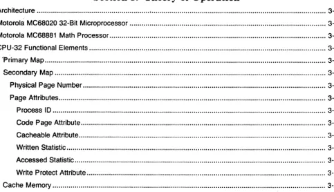
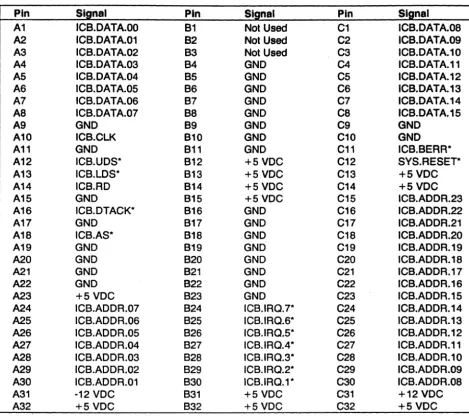
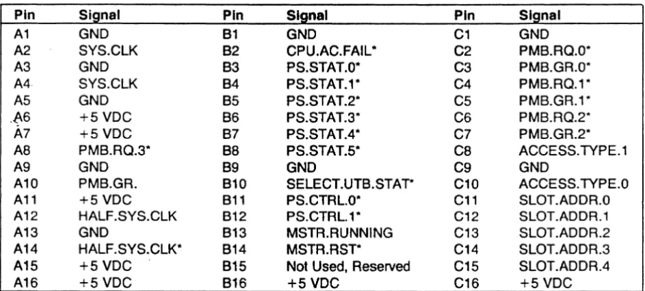
Plug One ... 5-1
Plug Two ... 5-3
Plug Three ... 5-4
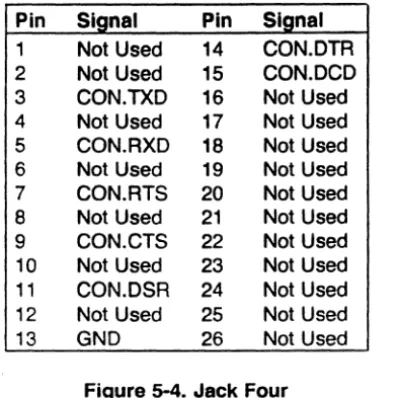
Jack Four ... 5-6
Plug Five ... 5-6
Functional Specifications
CPU32 - MC68020 Application Processor Board
Section One. Introduction
The Areta MC68020 Application Processor board provides a substantial increase In processing power to the Areta Series 1000. This board combines a full 32-bit Motorola MC68020 microprocessor and an MC68881 floating point coprocessor as a functional enhancement to the present 16-bit MC68000 Application Processor board.
In this application, the MC68020 operates at the full 12.5 MHz clock speed and drives a full 32-bit data path. The MC68881 floating point coprocessor performs math functions handed off by the MC68020. This shared-processing concept greatly reduces wait states and the amount of time required to run a given job. A single Areta 1200 system may contain up to four of these 12.5 MHz MC68020 Application Processor boards; and a single Areta 1100 system may contain up to two boards. In addition to having its own MC68020 microprocessor and MC68881 coprocessor, each board contains eight KBytes of high-speed cache memory without wait states, an MMU (memory management unit), a battery-backed hardware clock, a console port, a diagnostic port, and EPROM based self-diagnostics and boot routines. Each Application Processor board operates independently of the others, and shares a common pool of memory (up to 16 megabytes) over a high-speed 32 bit Processor Memory Bus.
MC68020 Microprocessor
The MC68020 microprocessor is an evolutionary enhancement to the MC68000. The MC68020 provides a full bit data path to complement the bit internal data structure. In addition, it features sixteen 32-bit general purpose and five special-purpose control registers, and a 32-32-bit program counter. It also includes a co-processor interface, eighteen addressing modes and a high performance 128 word on-Chip instruction cache. The MC68020 instruction set has been especially designed for high-level languages and ARIX, which is Areta's implementation of UNIX 5.2 for tightly-coupled shared-memory, multiprocessor systems.
MC68000 Compatibility
The system architecture of the Areta uses a proprietary 32-bit high speed bus structure that allows the MC68020 32-bit Application Processor to be used in a mixed mode with MC68000 Application Processors in any Areta system. When the two types of boards are used together, an MC68020 should be deSignated as the master processor. Any other Application Processor boards In the system, whether MC68000 or MC68020, must be designated as slave processors.
Thus, the user can selectively upgrade the Areta system to match a specific set of needs without limiting the'potential for future growth.
Cache Memory
Cache memory for the Areta's Application Processor cache permits it to run at full clock speed, since no wait states are incurred. Working out of cache reduces bus traffic and further improves system throughput. All reads from memory (whether instructions or data) are directed to cache memory; all writes to cache memory are written through to maintain cache concurrency throughout the system, The two-set cache is direct mapped, so each memory location can be written to only one cache location, Redundant tag bits are provided for both memory and the Application Processor, thus allowing monitoring of the Processor Memory Bus for updates without wait states.
Diagnostics
In addition to console support and a set of diagnostic LEOs on the front edge of the board, each Application Processor includes a status register, which allows it to continuously monitor environmental and power status of the system, Power on confidence tests are run from onboard EPROMs that perform a complete checkout of the Application Processor, automatic polling to check system configuration, and
cpu-s£
Functional Specifications
testing of the bus interfaces. A monitor is included for on-line debugging after the diagnostics detect a failure.
Memory Management
The Areta system provides two-level mapping to allow scatter loading of processes, and multiple protection modes. Physical memory pages are four Kbytes in size and may be set for read, write, code, data and page ownership protection within the MMU.
Configurations
Any Application Processor within a single cabinet may function as the Master Processor, by a simple switch selection. For best results, the MC68020 should be deSignated as the master If MC68020 and MC68000 boards are used in mixed mode. A load-balancing algorithm inherent to the Arete, allows all of the Application Processors (whether master or slave) to fully share the processing load.
CPU-32 Block Diagram
A block diagram of the CPU-32 is shown in Figure 1-1.
Figure 1-1. CPU-32 Block Diagram
Functional Specifications
CPU32 - MC68020 Application Processor Board
Section Two. Functional Characteristics
Performance
The MC68020 Application Processor board, with its full 32-bit data path, provides a substantial increase in performance over the MC68000 Application Processor board, which uses a 16-bit data path. In addition, the Integral cache memory for the Areta MC68020 Application Processor board permits it to run at the full 12.5 MHz clock speed, since no wait states are incurred for most cycles. The use of cache memory significantly reduces bus traffic to provide a further improvement in system throughput.
The MC68881 Coprocessor further extends the processing power of the system by performing computations handed off from the MC68020.
Specifications
SpeCifications for the MC68020 Application Processor board are shown in the following table:
MC6B020 Specifications
Processor 32 bit MC68020 running at 12.5 MHz
Cache 8 KBytes (no wait states) 80ns
Address Space 16 MB
Memory Management Proprietary Hardware Map
Page Size 4 KBytes
Floating Point MC68881 Coprocessor
Clock/Calendar Battery Supported, accuracy within 10 ppm
Diagnostics EPROM based Start-up and Run Time
Dimensions 14.437 inches (366,7 mm)x 15.75 inches (400 mm)
Connections DIN 41612 Plug and Socket
Section 9.
Functional Specifications
CPU32 - MC68020 Application Processor Board
Section Three. Theory of Operation
Architecture
This section provides a functional overview of the Aret~ CPU-321MC68020 Application Processor Board. The individual elements of the board and the functions and Interrelationships are described.
Motorola MC68020 32-Bit Microprocessor
In this application, the Motorola MC68020 microprocessor chip is defined as the CPU. The MC68020 has a full 32-bit data path. It executes at 12.5 MHz. with no wait states on most cycles.
Motorola MC68881 Math Processor
The Motorola MC68881 Math or Floating Point Co-processor is a physically a separate device, but it should be considered to be part of the MC68020, as they function as a single functional unit. In normal operation, the MC68020 fetches instructions and operands, and hands off the math-related operations to the MC68881. The MC68881 never takes control of the bus.
CPU-32 Functional Elements
The individual functional elements in this Application Processor are as follows:
Primary Map
-l' (
The primary mapper adds an offset value to ,tbeJligh order byte of the logical address for the CPU. The sum indexes an entry in the secondary map. The offset value for a process is contained in a register, which the supervisor may load at any time. This allows for a fast context switch between processes. There is one offset value for user processes, and one for the supervisor. The selection of which offset to use is made automatically at the beginning of each bus cycle.
The primary map hardware is complicated somewhat by a pair of registers, the CPPs (Current Page Pointers ). One register holds the most recently generated secondary map index for data. The other register is for the instruction stream read map index. These CPPs are invisible to software and do not affect the function of the primary map. The registers are included to speed up the map operation.
Secondary Map
The secondary map uses the map index from the primary map to look up a page entry. The page entry cont?ins a physical memory page number and some attribute information for that physical page.
Physical Page Number. The CPU-32 board can address 16 megabytes (MB) of physical memory. The pages contain 4 kilobytes (KB) each, and there are 4096 of them. Therefore, there are 12 bits of address in a page number.
Page Attributes. Each page entry has a process 10, some protections, and some statistics. The operating system may enable faults that can abort a process based on this data.
Process ID. The process 10 is compared against a value in the appropriate (user or supervisor) process 10 register.
Code Page Attribute. This bit identifies a page as executable only. Operand access of a code
7
I
v.(,4-}Jpage or execution of a non-code page may fault a process. . JC:>I"£
17A/
Cacheab/e Attribute. This bit enables cache-load. In normal operation, all pages are cacheable.
f.,::
~~61
Written Statistic. If statistic updating is enabled, then this bit is set by writing any location in the6'07d
cot
~ ~~~
Accessed Statistic. If statistic updating is enabled, then this bit is set whenever its page is accessed. The two statistics may be useful for page-replacement algorithms in a virtual memory operating system.
Write Protect Attribute. Set this bit to write protect the page. Cache Memory
The CPU-32 has eight kilobytes (8KB) of physical cache memory onboard. The MC68020 has 256 bytes of logical cache on chip for instruction words only.
The block size is four bytes. (Block size is the smallest unit of data that may be loaded on a cache miss.)
The cache is organized into two sets; there is a tag memory for each set.
-The cache is fast enough that most cache hits require no wait states. (One wait state is suffered when a program crosses a page boundary).
The cache data memory resides on a cache data bus that is isolated from the MC68020 data bus by a latching transceiver. This allows the cache data memory to be time-shared between the CPU and the updater without degrading CPU pertormance.
Updater
[,6
Gr
je..A
Lo.R
k
~This is a feature that monitors the PMB (Processor Memory Bus). The updater latches the address @d
"1
data written, and compares the address against the cache tags. (A second array of tag memory is provided for the purpose.) If the word is cached (this is considered to be an updater hit), then the updater writes the new value into cache. The updater ensures that all CPUs are using the same data at all times. The: ,Updater also keeps cached words current when the CPU writes partial words. (To allow
s.~lf test, the updater and cache may be enabled individually, but in normal operation they are both enabled together.)
CPU-32 Master Operation
All CPU-32 Application Processor boards have the same ICB circuitry installed, but some of it is only enabled on the master. A set of data tranceivers and address buffers drive the bus only when the master CPU selects the ICB address range. A PAL (programmable array logic) derives MC68000-like data strobes from the MC68020 address and size outputs. A mechanism (the TAS semaphore) on some liD
boards requires individual byte strobes, even on reads of the ICB bus. The PAL also synchronizes ICB.OTACK, a signal the selected ICB slave drives to terminate the cycle. A timer terminates an unacknowledged ICB cycle after about 20 microseconds (20us). An ICB timeout under these conditions results in a bus error.
CPU-32 Slave Operation
Each CPU-32 Application Processor board has ICB slave circuitry. The master CPU controls the slaves through it. If the board is not designated as a master, the board defaults to slave operation. This slave Circuitry is selected when the high-order ICB address bits
<
16 ... 23> match the slot number where the..
board is installed. This operation is identical to that of the MC68000 (except board 10).
Slave's Mailbox
A bytewide register (ICB command) may be written Into by the master. The slave may read it at any time, but normally it reads ICB command in response to the slave Interrupt flag.
Another bytewlde register (ICB status) may be written by the slave and read by the master. An Interrupt request flag (set by the slave at any time and cleared when the master reads ICB status) is-normally used to get the master to read it.
Another byte of ICB status may be read by the master. (The master may read both as a word.) This byte returns the board 10, and the status of the two ICB interrupt flags.
Slave Controls
A slave configuration register gives the master total control. The master can write a byte at any time. This register is cleared by a system reset (power-up, pushbutton, or master executing RESET instruction).
Two bits let the master'control the slave's HALT and RESET lines. To reset the slave, the master must clear both bits, wait 1 0 microsecond~, then set them both.
Two more bits control the PMB priority level the slave will use. Three bits control the ICB interrupt request level the slave will assert.
One bit, when set, causes a slave interrupt. The slave can clear this bit by reading its mailbox. Ports
Ports provided on the CPU-32 include serial ports, a timer, and a clock/calendar device.
Serial Ports
Serial ports are provided by a Zilog 8031. This device has two serial (asynchronous) channels. One is designated "console," and the other "modem," but they are identical, pin for pin. They can connect to an RS-232 terminal using the Arete console cable supplied with the system. The two connectors are mounted on the front edge of the MC68020 board, below the LEOs. These serial ports have their own built in bit-rate (baud) generators.
Timer
The timer function is provided by a Zilog 8036. This device has three timers, and some parallel 110 lines.
One timer is tl;le 60Hz interrupt, and the other two are spare. The parallel 110 is used to access the
ca.l~mdar device.
Clock/Calendar
The clock/calendar function is provided by an OKI 58321 device. This device has its own battery back-up and runs at all times. It keeps time in BCD format, with a separate register for each digit.
CPU-32 Operations
The operations in the following paragraphs describe subsystems and board-level functions that describe the operation of the CPU-32 in the Arete system.
Reset Subsystem
The reset subsystem is in a PAL16R4B. It allows the CPU RESET instruction to clear the bo~rd. If the board is a master, the RESET instruction goes out to the rest of the system. On-board reset (ON.BD.RESEr) is synchronized to the 6.25 MHz clock, to guarantee adequate setup time for those devices that require it. For example, the peripheral sequencer must be initialized by its forcing reset input, which requires a recovery time before the next clock edge. The ICB reset function requires that HALT and RESET be asserted simultaneously. This matches the function of the MC68000 CPU board. MC68020 Address Decoding
PAls on the MC6B020 CPU decode the address spaces based on address range, speed, and function. 4c (the register decoder) decodes onboard devices which are usable only by the supervisor. These are all fast enough to run with one wait state.
The 3c PAL (cycle terminate decoder) uses ON.BD.SEL* to acknowledge these devices.
The 5c PAL decodes size and space. It determines whether DSACK indicates a word- or long-word sized transfer. It also decodes the breakpoint acknowledge cycle BREAKPOINT., and the interrupt acknowledge CPU.AVEC*. These cycles are fully described in the MC68020 User's Manual.
The 6c (range decoder) PAL decodes memory space and the slow 1/0 ports: ICB, PROM, and the BOOO family devices. These devices each provide a separate acknowledge.
Size
The MC6B020 CPU emits SIZ<1,O> to indicate the size of the operand it would like to transfer. The system may end the cycle with BERR* or by DSACK<1,0>*. DSACK indicates the size of the device which completed the transfer. If the size was too small for the operand, the CPU makes another cycle to finish the job. If it was too big or just right, the CPU assumes the correct bytes were activated as selected by A< 1,0>.
The 5c PAL decodes the size of the selected device, word, byte, or long. There are now no byte size ports. Long is the default size, so only word size need be decoded. Size is gated into DSACKs.
Byte selects for memory (main and cache) are decoded from SIZ<1,O> and A<1,O>. ,
.
B~~ selects UDS and LOS are decoded for the ICB bus master, from SIZ and AO. MC68020 Cache Control
The cache is in 2 sets, selected by an address bit. Each set has a pair of tags.
2K xB RAMs with output enable are used to simplify write cycle timing. Output enable is on only when reading.
Byte selects are multiplexed by CPU.OFF, a signal which indicates the updater owns the bus. Updater byte selects are latched in the update compare state to extend the CS· setup time in the update cycle. WE· is gated outside the PAL to extend data and address hold time during a load or update.
CACHE.LOAD* is the signal which causes a new cache entry to be loaded. (A cache entry includes the data word (4 bytes), and primary and secondary tag words.) CACHE.LOAD occurs when a memory read misses cache.
- SectIon 8.
Mapper Operation
The MC68020 CPU board mapper is functionally similar to the MC68000 mapper, but operationally more complex.
A pair of CPPs (current page pointers) are used to retain the most recently used map offsets: data and code. This is because there is not enough time to do a no-wait (3 clocks) cache hit cycle if a new map offset is needed (it usually is not needed). When a new map offset is required, it's sampled. with the clock edge at 120. 74F161 or 163 registers are used for their load enable feature, because 74F377 is not available.
The critical delay path is to DSACK. DSACK<1,O>* is sampled on the falling edge of CPU.ClK, with tset of 10 and thold of 20. Thus, for a no wait cycle, both signals must be dropped by 110 into the cycle. DSACKs must be stable between 110 and 140, and 190 to 220.
PAGE.COMPARE" determines whether a new primary map (therefore a wait state) is required for the cycle. The delay path is U.FC.2* to OFFSET<0 ... 7> to SUM<0 ... 7> to PAGE.COMPARE* low if no new map is needed. PAGE.COMPARE* is ready by 91.5. If PAGE.COMPARE* is high at 91.5, a new map offset is clocked into one CPP at 120. The new map offset is valid at 139, and the new map is valid at 164. PAGE.COMPARE* falls between 125.5 and 147.
A latch samples PAGE.COMPARE* at 120 to stabilize it during the DSACK hold time. The latched signal lPGC" is valid at 99.5, and remains stable through 160.
The DSACK PAL uses 1WAIT* to determine which compare to use. Fault Logic Operation
Fault logic makes bus errors, and retains information for the operating system to recover. The Page Attribute Verifier (pav) enforces the page attributes by making PRIVILEGE.VIOLATION, which is ORed into CPU.BERR".
1. Hit at same page. In the no-wait cycle, if U.FCx switched from code to data or back, a new offset is enabled into the secondary map no later than 57, and attributes are valid (25 ns map RAMs) by 82. The pav output is valid by (15 ns pav PAL) by 97. The ACK PAL drops CPU.BERR* by 102 if there is a violation.
2. Hit at a new page. One-wait cycle with CPP update. MAP. OFFSET good by 135. Attributes by 160. Pav outputs by 175, BERR by 190, when it is sampled.
3. Miss. Many waits, for CPP update and PMB cycle. On a violation, the PMB sequencer is inhibited -by BERR and never starts. On a UC error, the fault is latched in with the data, sets
FATAL.MEM.FLT*, and becomes a BERR at the next 12 MHz clk.
For any bus error, the cause is available at the fault register inputs as the BERR begins. BERR sets ECK (fault register clock) on the same edge the MC68020 uses to latch in BERR. The fault data may then be read. The read clears ECK.
Processor-Memory Bus Sequencer
The PMB interface for the MC68020 is controlled by a state machine in two PAL 16R4s. This sequencer co-ordinates the action of the write accellerator, the import/export buffer, and the read interface.
The PMB interface is effected in 74F543 registered tranceivers. These chips have two transparent latches (window latches) connected in opposite directions between the two ports. The latches are transparent when the lExx* pin is low, and they latch up when lExx" rises. The 3-state outputs can drive a bus directly (sink=64ma).
The write accelerator enables the CPU to write (any size word) without waiting for the PMB arbitration. A holding register latches the write address and data.
There are five flags in the PMB sequencer:
1. PMB request: This indicates that the sequencer wants to get on the PMB.
2. BUSY.RD: This indicates that a read is underway, bus access has been granted, and the operation continues until PMB.CYC.DONE occurs.
3. PMB.WR.PNDG: This indicates that a write is in the accellerator; this flag turns on when the CPU
writes, and turns off with PMB.CYC.DONE for that write.
-4. PMB.ACK: This flag is the cycle end signal for PMB accesses. The ACK PAL uses it for DSACK. 5. WR.ACC.FULL: This flag indicates the WAB is full.
These flags are decoded by some gates and the 10r PBUS PAL to control the PMB interface parts. See the PBUS PAL listing for detail on this decoding.
The WAB control decodes STB.ACC, which
is shaped by WR.STB- for better timing accuracy. The resulting STB.ACCLRTR- latches data arriving on PMB data.
State Follower
The STF (CPU state follower) generates signals for synchronizing board operation. The STF is a finite state machine. Setup of an 'F74 is 3ns,
+
15ns for the PAL, gives a setup time of 18ns before the rise of 12MHz-. Hold time is less than zero ('F74 thold=1ns < min PAL delay).The machine is forced to a clear state between processor cycles so it will start in a known state. This forcing operation also ends the cycle if there is a bus error termination. .
The STF puts out SYNC.AS, CPU.WAIT, and CPU.S34. The cache bus grant signal CPU.OFF is generated in the cache control logic by a PAL16L8B and a fast register. The updater has the cache and PMB interface (CPU.OFF true) unless one of these conditions is true:
• State 34 of a cache hit.
• Even number (2,4, etc.) wait state of a write or read-miss. • Last four wait states of a read-miss.
• State. 34 of a test access of cache or tags.
The updater uses CPU.OFF to indicate when its requests have been satisfied.
The STF operates normally if a bus error with DSACK (cache hit with access violation) occurs. If there is no DSACK (cache miss with access violation, ICB timeout, or BERR), the STF is forced to a clear state when CPU.AS negates.
Tag Data
• PTO.DATA.<00 ... 11>
This is the primary Tag Data for cache set O. The tag data represents the physical page of a long-word in cache memory. That is, for a given word in the cache, the tag data says where that word is in main memory. The tag data word and the cached word together are called a "cache entry."
In the CPU-32 board, there are two cache sets. Each set (1 K x 32 bits) has a separate tag memory. In this way the CPU-32 can cache two words from different physical pages if those words are at the same address within their respective pages. The MC68000 board has only one set.
• PT1.DATA.<00 ... 11> Primary tag data for cache set 1. The primary tags are used to compare the CPU address to see if there's a hit on the current read.
• STO.DATA. <00 ... 11> Secondary tag data for cache set O. The secondary tags are used by the updater to compare the PMB address to see if updates are required on words that have been cached.
Section 9 .
• ST1.DATA.<00 ... 11> Secondary tag data for cache set 1. Updater Operation
The updater copies any PMB writes to cached words into cache.
There are three request flags: compare (a PAL a-pin), updateO, and update1 (F109).
Any PMB write strobes data, address and selects into the update latches (F543) and sets the compare request. CPUOFF determines ownership of the time-shared cache.
A CPU OFF with compare request set generates a compare state. The tags look up the PMB address, and COMPARE.ENB* allows the comparators to set one (or both!) update request. The critical delay path is 12MHZ* to CPUOFF to PMB.lNT.ADDR to STx.DATA to UD.HIT.xx to flag-Js to F109 tset to 12MHZ*. Because the delay path must be <80 ns, 35 ns tag RAMs are required. Notice that COMPARE.ENB* is not on the critical path.
Once an update request flag is set, any CPUOFF generates an update cycle. CPUOFF also asserts K to the request flags, clearing them at the end of the cycle.
ICB and PMB Bus Operation
ICB
The ICB connects to aU boards in the system. If more than one CPU is configured in a system, one CPU is designated as the master. The master CPU controls the ICB, using it to control the operation of the slave CPUs, and to monitor their status. The ICB reads and writes the OTB master 10 arbiter RAM. Note that each board slot connects to the ICB in the Arete Series 1000 system, and has a unique .64K byte segment of memory. Status and control registers for the board are located at the top of its memory segment. Each slot has a 5 bit hardwired slot address that determines which 64K byte memory segment the board occupies. Another location in the input/output segment, read through the ICB, gives the board type currently in that slot. At power up the master CPU reads the board type from each slot, so the system can configure itself automatically. The ICB has 16 data bits, 21 address bits, and a subset of the VME bus control signals.
ICB Data Buffers, Control
The 16-bit ICB data bus (ICB.OATA.0-15) is buffered with bidirectional transceivers. These devices are enabled when ICB address bits 16 through 20 match the slot address, the ICB address strobe (ICB.AS*) is active, and one or both of the ICB data strobes (ICB.LOS*, ICB.UOS*) are active. The direction of the buffers is determined by the ICB read signal, ICB.RO.
1/0 Decoders
The first level of address decoding is comparing the five bit board slot address with ICB address bits 16 through 20. If they match and ICB.AS· is valid, then ICB.SEL* is activated. Address bits 21 through 23 are not currently used and are pulled to logic level 1.
PMB
The PMB provides the 32-bit data path between main memory and the CPUs and OMA channels in the system. Up to four CPUs can dynamically share up to 16 megabytes of main memory on the PMB. The PMB includes 32 bits of data, 26 address bits, and control signals.
PMB Bus Arbiter
The PMB bus arbiter on the OMC accepts requests for use of the PMB by the various PMB bus masters. The highest priority requester is then granted use of the bus to transfer data to or from main memory. There are six request inputs for the PMB: 4 CPU requests, 1 OMA request (for the up to four DMA channels), and the refresh request. Following is a list of the PMB request priorities:
Device PMB Request Priority
Refresh
o
(highest)DMA channels 0-3 1
CPU 0 2
CPU 1 3
CPU 2 4
CPU 3 5 -<lowest)
These requests are activated on the rising edge of the PMB clock (25 MHz) by the various bus requesters, and are then synchronized again on the OMC by the PMB clock. The PMB arbiter uses one set of request and grant signals to interface with the four OMA channels.
The signal PMB.GO is active for the first five cycles of any PMB cycle, except in the case of a 32-bit write, where it is active for six cycles. The requester must not drive the PMB bus once its grant has been deactivated.
The PMB.CYC.DONE* signal is activated after the appropriate number of clock periods have elapsed to indicate the completion of the cycle. The following chart shows the number of PMB clock cycles, or states, required for each type of cycle:
Type of Cycle Number of Cycles PMB States
Refresh 8 SO- S7
32 bit write 8 SO - S7
Read with no error 10 SO- S9
Read with error 13 SO - S12
Read/ModifylWrite 15 SO - S14
The ReadiModify/Write cycle mayor may not be associated with an error condition. It is handled in the same way, whether there is an error or not. PMB.CYC.DONE* occurs during the last clock period of the cycle. The CPU uses PMB.CYCLE.DONE to latch data on a read cycle and the memory board uses it to return to an idle state and wait for the next cycle.
Function Codes
Two of the PMB function codes are driven onto the bus by the DMC. The function code state machine uses the PMB byte select lines, the PMB read signal, and the DMA read signal to determine the proper function code:
FNC.2* FNC.1* FNC.O* Description
0 x x Refresh
1 0 0 8,16,24 Bit Write(Read/ModifyIWrite)
1 0 1 32 Bit Write
1 1 0 Read(Up to 32 Bits)
1 1 1 No Operation
The other function code bit (PMB.FNC.2*) is dedicated as the refresh function code, and is derived from the refresh grant signal. These three function codes are used by the memory and CPU boards to determine the type of PMB bus cycle.
The PMB.UC.ERR* signal goes active during S10 if an uncorrectable error occurs during a read or RMW cycle. It stays active until PMB.CYC.DONE* occurs, and is used by the CPU board to generate a bus error for the CPU. The PMB.ANY.ERR signal is active during S9 of a read or read/modify/write cycle that
h~ ·a correctable or uncorrectable error. PMB Cycle Descriptions
The CPU-32 uses three types of PMB cycles:
1. Write Cycle - Write cycles always use the PMB, even if the physical address hits cache. An MC68020 write cycle causes both address (including byte selects) and data to be latched into a ''write accelerator" circuit. This write accelerator holds data while waiting for access to the bus. The CPU may continue executing until it needs the PMB again.
2. Read and Miss Cycle - Any read of a location that has not been cached requires the PMB. The CPU waits until the cycle is completed.
3. Write by any CPU - This cycle activates the updater.
The following is a state-by-state description of each type of PMB cycle.
32 Bit Write Cycle
SO-2 CPU REQUEST goes active(2 cycles before SO).
SO-1 REQUEST is synchronized to PMB.CLK so it can be sampled by the arbiter state machine on the next clock edge(1 cycle
before SO).
SO GO, GRANT go active. CPU or DMC drives address and data on the bus.
S1 address, data, byte selects, and PMB.RD are valid on the bus. The DMC data buffers are enabled so check bit generation can begin.
S2 write function code is driven onto the bus. Grant code, byte selects, and data are latched on the DMC.
S3 the DMC drives generated check bits on the bus.
S4 function codes disabled. DRAM WRITE ENABLE goes active on memory board.
S5 DRAM WRITE ENABLE still active on memory board.
S6 disable GRANT and GO. CPU disables its address and data drivers.
S7 CYCLE DONE active.
SO disable data buffers and check bit buffers. Activate GO and GRANT for the next cycle, if back to back.
Read Cycle With No Error
SO-2 CPU request goes active(2 cycles before SO).
SO-1 request is synchronized to PMB.CLK so it can be sampled by the arbiter state machine on the next clock edge( 1 cycle before SO).
SO GO, GRANT, and CYCLE START go active.
S1 ADDRESS is driven by the CPU or the DMC. BYTE SELECTS, and PMB.RD are driven by the CPU only on a CPU read.
S2 read function code driven onto the bus. Grant code and BYTE SELECTS are latched by the DMC.
S3 Address is latched in error address latch or in the DMC in case of an error.
S4 function codes disabled.
S5 float GRANT and GO.
S6 memory board starts driving the data and check bits on the bus.
S7 RAM data and check bits are both valid at this time. The DMC latches data and check bits and prepares to start correcting the data in case there is an error.
sa
DMC checks data for any possible error.S9 activate CYCLE DONE. The CPU board latches the data on the next rising edge of the PMB clock.
so
disable data buffers and check bit buffers. Activate GO and GRANT for the next cycle, if back to back.Read Cycle With Error
9-11
SO-2 CPU request goes active(2 cycles before SO).
SO-1 request is synchronized to PMB.CLK so it can be sampled by the arbiter state machine on the next clock edge(1 cycle before SO).
SO GO, GRANT, and CYCLE START go active.
S1 ADDRESS is driven by the CPU or the DMC. BYTE SELECTS and PMB.RD are driven by the CPU only on a CPU read.
S2 read function code driven onto the bus. BYTE SELECTS are latched on the DMC.
S3 EDAC check bit output buffer disabled. Address is latched in error address latch in case of an error.
S4 function codes disabled.
S5 disable GRANT and GO.
S6 memory board starts driving the data and check bits on the bus.
S7 RAM data and check bits are now valid. The DMC latches data and check bits and prepares to start correcting the data in case
S8
S9
S10
there is an error.
The DMC checks data for errors.
set the PMB.ANY.ERROR condition. Activate errors and enable the output check bit buffer of the EDAC chip to get the syndrome. Change direction of the check bit buffer.
activate PMB.UC.ERR if an uncorrectable error has occurred. The
error syndrome is now valid and latched on the DMC. The memory board stops driving data and check bits at this state. The DMC changes direction of data buffers to prepare for driving
corrected data onto the bus.
S11 the PMB data bus is now floating, and the DMC data buffers are enabled to drive the corrected data onto the bus.
S12 activate CYCLE DONE. The CPU board latches the corrected data on the next rising edge of the PMB clock.
SO disable data and check bit drivers. Disable EDAC chip data and check bit outputs. Activate GO and GRANT for the next cycle,
if back to back.
Read/Modify/Write Cycle With or Without Error
SO-2 CPU request goes active(2 cycles before SO).
SO-1 SO S1 S2 S3 S4 S5 S6 S7 S8 S9 S10
request is synchronized to PMB.CLK so it can be sampled by the arbiter state machine on the next clock edge(1 cycle before SO).
GO, GRANT, and CYCLE START go active. The CPU board drives address and data on the bus.
address, new data bytes, byte selects, and PMB.RD are driven by the CPU.
RMW function code driven onto the bus. Grant code, byte selects and data are latched on the DMC.
EDAC check bit output buffer disabled. The address is latched in error address latch in case of an error.
function codes are driven false.
GRANT and GO are driven false. The CPU board disables its address and data buffers.
memory board starts driving the data and check bits on the bus.
ram data and check bits are now valid. The DMC latches the data and check bits and prepares to start correcting the data in
case there is an error.
The DMC checks memory data for errors.
The DMC latches the corrected data.
activate PMB.UC.ERR till end of cycle if one has occurred. If an error has occurred, the DMC latches the syndrome. The memory board stops driving data and check bits at this state.
Refresh
The DMC merges the memory data and the CPU write data using the byte selects, which indicate which bytes the CPU is
changing.
511 the PMB data bus is now floating, and the data and check bit buffers are enabled to drive the merged data onto the bus.
512 data and check bits are valid on the bus 10 nsec after the rising edge of 512. The memory board activates DRAM WRITE ENABLE haHway through this state.
S13 DRAM WRITE ENABLE is still active on the memory board. Check bits are latched in the 'last check bits written' latch.
S 14 activate CYCLE DONE.
SO disable data buffers, disable check bit buffers. Activate GO and GRANT for the next cycle if back to back.
SectionS.
The dynamic RAMs used on the memory boards must be refreshed a minimum of 256 times every four milliseconds. The signal PMB.RFSH.RQ* is a request for a PMB cycle from the PMB arbiter. Every 15.36 microseconds the refresh generator requests the PMB bus. When the PMB arbiter grants the request with the signal PMB.GR.RFSH*, the output of an a-bit refresh address counter is enabled onto the PMB address bus bits 2 through 9. The memory boards detect the refresh function code, and perform a refresh cycle. When PMB.GR.RFSH* goes inactive, the address driver is disabled and the refresh address counter is incremented in preparation for the next refresh cycle.
System Timing Generation
The bus operates synchronously at 25 MHz. On the DMC the output of a 50 MHz oscillator is first divided by two producing a 25 MHz clock (SYS.CLK). The 25 MHz clock is then divided again to produce a 12.5 MHz clock (HALF.SYS.CLK), which is used by the CPU board(s). Clock phasing is important to guarantee synchronization of the various system components. Both SYS.CLK and HALF.SYS.CLK rise on the same edge of the 50 MHz oscillator output, because of final synchronization with the 50 MHz clock ..
CPU-32 Data Transfer Operations
The operation of the CPU-32 may be described as a sequence of data transfers. Data may reside in a storage location. Storage locations are considered to be registers, including the special case of a memory location. When data is copied from one register to another, a data transfer occurs. Some data transfers take place by way of a holding register that functions as an intermediate storage location. These transfers are considered to be buffered, and may be subdivided into partial transfers into and out of the holding register. There are a number of different types of data transfers that the CPU-32 may execute:
1. A read from PROM.
2. Cache-as-memory, or cache test read,
a. Load importer from cache.
b. The MC68020 (uP) reads the importer.
3. Cache-as-memory write,
a. Load exporter from the MC68020 (uP).
b. Load cache from exporter.
4. Primary (master CPU) tag test read.
5. CPU tag write.
6. Secondary (updater's) tag test read.
7. Secondary tag test write.
8. Read multiplexed peripherals (timer, console, RTC).
9. Write multiplexed peripherals.
10. Read or write FPU (MC68881).
11. Control register load,
a. Miscellaneous registers: MMU offset, 10, enable, LEOs. ICB mailbox.
b. ·Address translation table read/write.
12. ICB read, write.
13. Fault register read.
1~. Main memory write,
a. Load Write Accelerator Buffer.
b. Write cache if hit and cache enabled.
15. Main memory read,
O. Wait for mapper and empty WAB.
a. If miss or cache disable, load WAB and request bus.
b. Wait for done. latch bus data.
c. Load importer (and cache if cacheable page).
d. uP reads importer.
16. Cache hit,
a. Page compare.
b. Load cpp if page compare misses (costs a wait state). c. Load importer, up reads importer.
17. Updater,
a. Update acquisition. b. Update compare. c. Update write. 18. Autovectors. 19. Bus error,
a. Access violation.
b. Uncorrectable memory error (error flag acquire). c. ICB timeout.
d. FPU timeout.
Timing Diagrams
The following timing diagrams show the relationship between the various CPU-32 signals:
• Update Compare State.
• Cache Hit, Page Match, No Violations, New FC (a no-wait state).
• Cache Hit with CPP Update.
• Best Case Miss and Load.
• Fastest Miss with Updater Activity.
Memory
User Memory.
Functional Specifications
CPU32 - MC68020 Application Processor Board
Section Four. CPU-32 Programmer's Model
Section
4.
The user memory area extends from 0 to OxFFFFFF, located in the complement of main memory board(s) that are installed. The user cannot control caching.
Supervisor Memory.
The supervisor accesses the same memory area as user from OxO to OX3FFFFF. To access the remaining 12 megabytes of the user space, the supervisor must use Move to Alternate Address Space (MOVES), or go through the map. Supervisor space above Ox400000 contains the test and I/O features, and main memory is in Ox800000-FFFFFF.
PROMs.
At power-on or any reset, 128 kilobytes of PROM begin at location O. These PROMs may be disabled by setting bit 3 in the "system port." The four PROM sockets are arranged at the top center on the component side of the Application Processor board assembly (Arete pin 50-01427). The locations and addresses of the four PROMs are as shown in the diagram below.
location 6d diagnostic, odd byte
Ox1 0001-0x1 FFFF location 6f monitor, odd byte OxOOOO01-0xFFFF
location 6g
diagnostic, even byte OxOO1000-0x1FFFE
location 6j monitor, even byte OxOOOOOO-OxFFFE
Test and
1/0
Features
Cache As Memory.
The memory area from Ox400000 to Ox401FFF, In the MC68020 cache, may be used as read/write memory. Repeating images of the same storage extend from Ox402000 to Ox41FFFF.
Data Path to Tags.
The four tag memory blocks may be tested from Ox4COOOO to Ox4C3FFF. Each tag memory occupies 4KB(Ox1000 bytes). You cannot write single bytes in a tag entry, only words or Iongwords. Do not write words to the unused word (odd address), because it may alter the even word in future revisions of the CPU-32 board. Each tag entry occupies 1 longword in the memory space, but only 12 bits actually respond as memory. The tag bits appear in the longword as shown in the two following diagrams:
31-+-28 27---+---16
not used ta bits
typical addresses:
<
---Ion<
---word Ox4C1 000--->The not used area writes nothing and reads unpredictably.
The four blocks of tag are arranged:
1. 4COOOO to 4COFFF: Set zero tag for CPU cache hits
2. 4C1000 to 4C1 FFF: Set zero tag for updater cache hits
3. 4C2000 to 4C2FFF: Set one tag for CPU cache hits
4. 4C3000 to 4C3FFF: Set one tag for updater cache hits Note that there are 001000 (Ox400) tag entries in each block.
Februarll
4,
198615---+---0 not used
MMU Registers
Primary Map Registers.
These four registers are write-only bytes.
Section
4.
Offset Register. The byte-wide system offset register at Ox4AOOOO contains an offset which is
added to supervisor logical addresses (if the mapper is enabled). The user offset register at Ox4A0002 adds to user logical addresses. Each offset register looks like the following:
Ox4AOOOO Ox4A0001 Ox4A0002 Ox4A0003
10 Register.Each 10 register looks like the following:
Ox4A0008 Ox4A0009 Ox4AOOOA Ox4AOOOB
system offset user offset
system 10
user 10
Process IDs are limited to the range O-Ox7F. If bit 7 is a one, the process 10 fault always occurs. The system process 10 register at Ox4A0009 contains 7 bits identifying the current system process. The user process 10 register is at Ox4AOOOB.
Secondary Mapper.
The secondary map is a RAM lookup table. Each entry looks like the following:
31+28 27 ---+---16 15+12 11 10 9 8 7 6---+---0 not
physical page not c c w a w process
used used p b t c p 10
The not used bits ignore writes, and read unpredictably.
The physical page field contains the high order address bits that select a page of physical memory.
The code page; bit cp marks the physical page as containing code. This page attribute is used for the . coc;teaccess fault.
The cacheable bit cb enables cache loads for that page.
The written statistic wt reports whether a page has been written into. The statistic is only updated if page statistics and the mapper are enabled.
The accessed statistic BC reports whether a page has been accessed.
The write protect wp attribute determines whether the user may write into the page. If the mapper is enabled, this bit can cause the write protect fault.
The secondary mapper occupies 16KB of supervisor memory as follows:
31---0 Ox483FFC logical page OxFFFOOO-OxFFFFFF Ox483FF8 logical page OxFFeOOO-OxFFEFFF
...
Ox480800 logical page Ox200000-0x200FFF
...
Ox480400 logical page Ox100000-0xl00FFF
...
Ox480040 logical page Ox010000-0xOl0FFF
...
Ox480008 logical page OxOO2000-0xOO2FFF Ox480004 logical page OxOOl OOO-OxOOl FFF Ox480000 l()9ical p~e OxOOOOOO-OxOOOFFF
There are also 7 images of the map table from Ox484000 to Ox49FFFF.
Control Functions
The various features described in the following paragraphs are enabled by write-only bytes.
LEOs.Some LEOs are under software control. A byte at Ox4A0004
address Ox4A0004
has 2 directly controlled LEOs (sl. sO). and 2 encoded LEOs. Write a 0 to light sl or s2. This register is cleared at power-up or by a RESET instruction.
Mapper and Fault Enable.There are six bits at Ox4AOOOE
address Ox4AOOOE
that enable the mapper mp, enable page statistics update ps , enable bus error on a process id fault mismatch id (page table entry not equal to process id register), enable bus error on a write to a write-protected page' wp, enable bus error on an instruction fetch from a data page ct, and enable bus error
Or"f a data access to an execute page df.
Section
-I.
System Port. This byte-wide write-only register enables various functions.
address Ox4EOOOO
Bit 7 is unused. The ae enables the level 7 interrupt for AC failure. The up enables the upd~ter. The updater should be enabled and disabled simultaneously with cache for normal operation. (Some diagnostics may enable one without the other to simulate cache or updater failure.) The ch enables cache. This bit actually controls the three functions below:
1. It enables loading of a cache entry (tag and cache) on a miss.
2. It enables cache hits (a read of a cached word does not use the PMB).
3. When cache is disabled (write a 0). the Next Load flip-flop is forced clear. Therefore. the first cache load when cache is enabled is always be into set zero.
A zero in pr enables the PROMs. The PROMs occupy 0 to OxFFFF in the supervisor space when they are enabled. The user can never access PROM. The us is the Utility read multiplex control. The pwr are two bits that control the power supply. This register is cleared either at power-up or by a RESET instruction.
ICB Registers
Slave Registers.
There are two registers at Ox4E0004, the Slave Command register and the Slave Status register. The -(write-only) Slave Status register can be read by the ICB master; the (read-only) Slave Command register is written by the ICB master. This action by the master interrupts the MC68020 CPU. When the CPU reads Ox4E0004, it clears the Interrupt request.
Slave Interrupt.
A write to Ox4E0006 triggers an ICB interrupt request. The slave cannot determine the level from which this interrupt is issued. The data written at Ox4E0006 is ignored.
Bus Fault Register.
A read-only register at Ox4E0007 can report the cause of a bus error.
Bus Error Events. The Bus Fault register latches the cause information when a bus error
occurs. It remains latched with that information until the program reads it. Reading frees the register to look for the next fault, but it does not alter the register's current contents.
If a second bus error occurs before the Fault register has been read, the new fault information is lost. This may confuse users of the MC68020, because the processor may receive a bus error due to a prefetch, but it does not process the exception if the prefetched data is never used. The Bus Fault register cannot detect an unused prefetch, so it always latches the fault data. In such a case, the Bus Fault register contains meaningless data, and is locked up unable to latch bus faults as they occur.
Bus Error Data. The register captures the following bits during a faulty bus cycle:
7 6 5 4 3 2 1 0 address
icb icb fatal data code wrt proc.
Ox4EOOO7 x
tim ber PMB fit fit pr 10
The x bit is unused. The Icb tim timeout bit Indicates an ICB access ended with no response. The icb ber ICB bus error bit indicates the ICB access ended with ICB bus error. The fatal PMB bit indicates multiple wrong bits in main memory caused an uncorrectable ECC error at the location of the fault. The code fit fault indicates attempted execution of data. The data fit fault indicates an attempt to read or write instruction text. The wr prt fault indicates an attempt to write to a protected page. The proc 10 fault is due to an 10 mismatch. The process was accessing a page assigned to some other process.
Section
4.
Peripherals
The timer, serial ports, and a calendar module can be accessed by the supervisor.
Serial
Ports.
At Ox500000, the Zilog (AMD, SGS) 8031 Async Dual Comm device provides a console (channel A), and a modem port (channel B).
Timer.
At 0)(508000, the Zilog 8036 Counter 1/0 device provides a 60 Hz interrupt timer, two spare timers, and a port for the calendar module.
Calendar Module.
The Oki MSM 58321 clock/calendar module is available through the parallel ports on the 8036. The 58321 keeps the date and time in BCD format, and has battery backup. The device is automatically isolated from the CPU whenever AC power fails, and during both reset and power off.
The 58321 requires the ports on the 8036 to be configured as shown in the following table. Each line from the 58321 is wired to one of these 8036 'bit ports."
7 6 5 4 3 2 1 0
port A not used data bits
out always out when writing, otherwise in
In the following table, "in" and "out" represent the direction of data travel through the pins on the 8036:
7 6 5 4 3 2 1 0
portB not used zero busy sel addr read wrt
out in in out out out out
For example. port B pin 0 must be programmed as an output. Port A transmits data to the 58321 for any write (including the register pointer), and receives it during reads. Port B controls access of the 58321, and should be configured as shown and left that way. The details of each line are as follows:
-1-7
Data Bits. These four lines load the register pointer and communicate with the registers. They must be programmed inputs whenever a read is in process (read is high); they must be
progr~l)1med outputs with valid data whenever either write pulse is being formed.
Zero. The zero bit reads zero if the 58321 is installed, otherwise it reads one.
Busy. This input reads zero if the date and time may be changing, and reads one if the data is stable and may be read or written. The busy indication begins 244 microseconds (244 us) before the data actually changes, and ends when the new data has stabilized. During busy. data writes do not work.
If necessary. you can read the data during busy. Read the register set twice, and compare the results. If they are equal, the data is valid. Do this read and compare for the whole register set; don't compare register by register.
Se/. This output bit enables the 58321 to make data transfers. Program a one to enable; send a zero to protect the 58321 state. The 58321 does not recognize addresses or anything if sel is at zero. This bit must be stable throughout any transfer. Since this bit is an enable signal (an address qualifier), not a strobe (a timing signal), it may be left on during an entire access sequence.
ICB Programming Considerations
Master CPU
The Arete ICB address locations are from Ox600000 to Ox7FFFFF.
Register Access. All CPUs have registers that are accessible by the ICB master. These registers are selected according to the slot location of the CPU. The master selects Ox6?FFFC, for instance, where? is the slot number.
Configuration Port. All CPUs (master or slave) have a configuration port which the ICB master
must set up. This word is configured as follows:
15
I
14I
13I
12 11J
10 9 8 7---+---0 rI
hI
iI
priI
level commandOx6?FFFE Ox6?FFFF
Note that in the table above, rand h are the RESET and HALT lines controlling the slave. To reset the slave, clear both of them, wait more than 10 microseconds (40 NOPs), then set them.
The i interrupts the slave (write 1 to interrupt).
The two pri bits determine PMB priority.
The three level bits determine which level ICB interrupt the slave issues.
The command is a byte which the slave can read.
Status and Board /D. This word reads as follows:
15
I
14I
13--+--9I
8 7---+---0 siI
miI
00101I
s statusOx6?FFFE Ox6?FFFF
Note that the si bit indicates a pending interrupt to that slave; the ml bit indicates a pending ICB interrupt from that slave; the 00101 indicates an MC68020 board type; and the s bit indicates the board is a slave. The status byte is loaded by the slave. This word may be read as bytes or whole. Reading the status byte clears any pending ICB interrupt request.
Slave CPU
All CPUs have the slave ICB interface. A mailbox register may be read at Ox4E0004 (clearing the slave interrupt flag).
A slave status byte may be written into Ox4E0004 so the master can read it. A write to Ox4E0006 sets the ICB interrupt request flag for the slave. (This flag will be cleared by the master.) Consistent with the operation of the MC68000 CPU, the slave cannot poll its ICB interrupt request flag.
Interrupts
The interrupt scheme for the MC68020 board resembles that of the MC6S000 board. The only hardware interrupts are the seven autovectors.
CPU-9£ FunctionalSpecijications
Addr. This output bit strobes a register pointer value into the 58321. To strobe the value, follow these steps:
1. program port A to be outputs. 2. write the register number into port A. 3. set "addr" to one.
4. set "addr" to zero.
Read. This output bit enables data from the currently selected register to appear at port A. To read data, follow these steps:
1. program port A to be inputs. 2. set "read" to one.
3. wait 6 us for access time (for example, read port A ten times). 4. read the data from port A.
5. set "read" to zero.
Wrt.
This output bit strobes write data into the currently selected 58321 register. To strobe the data, follow these steps:1. program port A to be outputs. 2. put the data in port A.
3. set "wrt" to one.
4. wait 2 us (read port A three times). 5. set "wrt" to zero
Interrupts to a Slave
Interrupts to a Master Level
7
6 5 4 3 2
1
Level Mode Remarks
7 Autovector Power Fail.
6 Autovector Timer.
5 Autovector Interrupt From Master CPU.
4 Autovector Serial Ports.
3 Autovector Not Used. 2 Autovector Not Used. 1 Autovector Not Used.
Mode
Autovector Autovector Autovector Autovector Autovector Autovector Autovector
Remarks
Power Fail. Timer.
ICB Interrupt Request Five.
Serial Port or ICB Interrupt Request Four. ICB Request.
ICB Request. ICB Request.
MC68881 Coprocessor Programming Considerations
The MC68881 Coprocessor is an FPU (floating point unit) that appears, to user programs, to be part of the MC68020. This MC68881 device functions as a true coprocessor, performing math operations handed off by the MC68020 and saving processing cycles for the MC68020. The device effectively shares the system processing load, but never takes control of the system. The device has eight 80-bit registers for internal operands.
In actual operation, the MC68881 provides a functional extension of the MC68020 instruction set, adding data _ types, registers, and instructions. If the device is not installed, then execution of any of its Instructions results in the F-line exception, vector number 11.
RESET Operatlon.The MC68881 can be reset by any of the following: • power-on.
• slave reset or system reset.
• execution of the RESET instruction.
Be carefu when using the RESET intruction, because the Internal state of the FPU is los
Downloading Code to the GC/IOCP
The MCPU (master CPU) initiates the download of code from the MCPU to the GC/IOCP (general purpose input output control processor). The MCPU initiates the procedure by issuing a download command to the GC/IOCP to the ICB Interrupt Register, and interrupting the GC/IOCP at the same time. The GC/IOCP echos the download command back to the MCPU to indicate it is _ ready to continue. The MCPU then accesses the virtual register and reads the information in BD_MEMST and BD_SZMEM. This information tells the MCPU where (in the remaining memory) the code to be downloaded can be inserted.
Once the MCPU has the information, it must build an ICB command header at the lowest address of free memory. The command header fields are as follows:
Command, status, destination, source, information and count.
The MCPU writes via the command IWMCMD (write memory command). The status must be zero (0); the destination must contain the slot in which the GC/IOCP is installed (in hex), the information field must contain the final target address of the downloaded code (where it is to reside) and the count (in bytes) reflects the length of the code that follows the header.
If the code to be downloaded is too large for free access memory space, it must be downloaded in segments. Note that the MCPU can access only the 64K dual-ported memory on the GCIIOCP. If segment loading is necessary, the low 32K of program (including interrupt vector table) must be loaded last.
Next the MCPU must cause the icbcmdhdr pointer in the virtual register structure to point to the command header.
At this point, the GCIIOCP board must be accessed to obtain the command information and move it to the desired location. The IMEMCMD (process a memory-resident command packet) is sent to the interrupt register of the GCIIOCP. When the GCIIOCP echos the same IMEMCMD back to the MCPU, the MCPU checks the status field in the ICB command header for the command complete status
ICMPLT, indicating the command was executed.
The above procedure of building the ICB command header and entering code is repeated, as needed, to download the entire block of code. The command header of the last piece of code to be downloaded (bottom 32K with interrupt vectors) must contain the IWJCMD command in place of IWMCMD. This tells the GCIIOCP to write the code to the final target address and jump to the entry point (second address in interrupt vector table).