This is a repository copy of Two level, in-band/out-of-band modelling RF interference
effects in integrated circuits and electronic systems.
White Rose Research Online URL for this paper:
http://eprints.whiterose.ac.uk/91080/
Version: Accepted Version
Proceedings Paper:
Whyman, N. L. and Dawson, J. F. orcid.org/0000-0003-4537-9977 (1999) Two level,
in-band/out-of-band modelling RF interference effects in integrated circuits and electronic
systems. In: EUROEM 2000, Euro Electromagnetics, Edinburgh, 30th May - 2nd June
2000. , pp. 135-139.
https://doi.org/10.1049/cp:19990258
[email protected]
https://eprints.whiterose.ac.uk/
Reuse
Items deposited in White Rose Research Online are protected by copyright, with all rights reserved unless
indicated otherwise. They may be downloaded and/or printed for private study, or other acts as permitted by
national copyright laws. The publisher or other rights holders may allow further reproduction and re-use of
the full text version. This is indicated by the licence information on the White Rose Research Online record
for the item.
Takedown
If you consider content in White Rose Research Online to be in breach of UK law, please notify us by
TWO LEVEL, IN-BAND/OUT-OF-BAND MODELLING RF INTERFERENCE EFFECTS IN INTEGRATED CIRCUITS AND ELECTRONIC SYSTEMS
N. L. Whyman, J. F. Dawson*
SASD, DERA, Farnborough, UK and *University of York, UK
Abstract –In this paper we present a new behavioural model that combines high frequency and low frequency subcircuits to predict the effect of Radio Frequency Interference (RFI) on linear integrated circuits. The model is constructed from measured and manufacturers data, and can determine the failure mechanisms in analogue systems subjected to RFI. The results of measurements and simulations of circuits containing one and two op-amps demonstrate the principle of the model.
INTRODUCTION
Much work has been done previously to characterise the effects of electromagnetic interference on operational amplifiers and other circuits [1]-[6]. Little attention has been given to addressing the problem of a system with more than one element (i.e. op-amp). Here we present a two-level macro-model (Figure 1) that uses a linear scattering parameter model to represent the interference propagation as a High Frequency (HF) subsystem. A non-linear frequency dependent function is used to generate offset voltages that are injected into the Low Frequency (LF) part of the model.
The HF subsystem is characterised by a scattering matrix measured using an Integrated Circuit test jig. It was modelled directly in the frequency domain by the PSpice circuit simulator program [7]. The voltages
generated in the LF subsystem are determined
experimentally by injecting RF into the IC terminals. Sets of polynomial functions of frequency and incident power, for the offset voltages, are then determined. The approach presented allows the prediction of the RF propagation and the effect of interference on electronic systems. Modelling the HF propagation in frequency domain avoids the difficulty of simulating the wide disparity in the frequency ranges between the out-of-band interference and the operating signals in the circuit.
Smn Smn
HF LF
PRFin
PRFout1
IC1 IC2
PRFin2
PRFout2
VRF VRF
Fig. 1: Two layer model showing coupling between HF and LF layers
THE LINEAR SUBSYSTEM
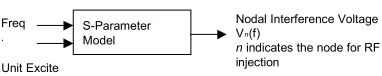
S-Parameter Model Freq
.
Unit Excite
Nodal Interference Voltage Vn(f)
nindicates the node for RF injection
Fig. 2 The Linear subsystem, the High Frequency component
The linear model Figure 2 is determined from the measured scattering parameters of the integrated circuit. It has been found that above 100MHz the scattering parameters are virtually independent of the operating conditions of the IC (Figure 3).
Fig. 3 Scattering parameters measurements with operating conditions device powered ON or OFF A subcircuit can easily be implemented in PSpice using the measured S-parameter values [8]. Figure 4 shows a
2-port S-parameter subcircuit. PSpice allows the
voltage-controlled voltage sources, E11, E21, E12, and E22, to use the measured S-parameters, as a gain parameter, directly in the form of a text file of Frequency (Hz), Magnitude (dB or raw), and Phase (degrees).
Fig. 4: S-parameter subcircuit schematic
This paper is a postprint of a paper submitted to and accepted for publication in the proceedings of "Electromagnetic Compatibility, 1999. EMC York 99. International Conference on and Exhibition on" and is subject to Institution of Engineering and Technology Copyright. The copy of record is available at IET Digital Library:
[image:2.595.314.505.177.215.2] [image:2.595.313.515.318.458.2]In Figure 4
V
1andV
1are the amplitude of the forward and backward travelling waves, respectively.Considering the incident wave
V
1, R1N and Rs willcancel {50+(-50) = 0} such that
s
f
V
V
1
(1)
and the sources E11 and E12 have no influence on
V
1f.By definition
V
1
V
s/
2
so that the voltage source E11 will have a value of11 1 11
2
V
S
E
(2)which generates a reflected wave component of half that
amplitude (
V
1S
11) as required. If the effect of E12 is also considered then12 2 11 1 12 11 1
2
E
2
E
V
V
S
V
S
(3)Which is the desired result.
In a similar manner the scattered voltage at node 2 is
21 2 22 2 21 22 2
2
E
2
E
V
V
S
V
S
(4)where
V
2 andV
2
are the amplitude of the forward (toward the node) and backward (away from the node) travelling waves at node 2
The circuit can be expanded to any number of input/output pins by adding additional dependent sources – Figure 5 shows the n-port sub-circuit for any number of pins.
Fig. 5: An n-port S-parameter sub-circuit expanded for any number of pins (Pinn). The device can be modelled, for HF propagation, using the n-port S-parameter sub-circuit and implemented in PSpice by a circuit schematic as shown by Figure 6. The two voltage sources EG3A and B are used to excite the
circuit whilst allowing the reflected wave to be detected at node 11 (S11). All other pins on the device have matched terminations and the transmission coefficient is determined from the voltage at each termination (e.g. S21).
Fig. 6: PSpice circuit schematic of device
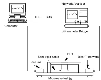
[image:3.595.78.288.95.392.2]Linear parameter measurement
Figure 7 shows a block diagram of the test set up to measure the devices linear characteristics (scattering parameters) using a network analyser.
Computer
Microwave test jig DUT
Bias 'T' network Semi-rigid cable
dc Bias IEEE BUS
RAB O/P
S-Parameter Bridge Network Analyser
Fig. 7: Linear (S-parameter) measurement block diagram.
To carry out these measurements, jigs were designed for both dual in-line (DIL) and surface mounted integrated circuit devices (SMD) [9]. Both jigs were designed to accommodate devices with a maximum of 16 pins. In the DIL jig each of the 16 input lines was constructed using semi-rigid coax to couple signals between a bias 'T' network and the pin of the device under test. In the SMD jig each of the 16 input lines were constructed
using Microstrip line, of 50 characteristic impedance,
[image:3.595.309.515.134.263.2] [image:3.595.327.499.381.518.2] [image:3.595.79.286.470.640.2]The scattering matrix is constructed by using two port
S-parameter measurements between each pair of
terminals. In practice above a frequency of 100MHz the
devices are reciprocal, that is the S-parameter
magnitude is the same for the measurement
12 21 S
S , which greatly reduces the number of
measurements required (Figure 8).
Fig. 8 Scattering measurements between pins 3 and 6 showing the reciprocity of a device For the linear characterisation of the device the measurements were carried out using the surface mounted device component test jig. The Integrated Circuit device used in the HF subcircuit model was the
Surface Mounted Device TL061CD JFET-input
Operational Amplifier. To characterise the scattering matrix of the device the RF signal is injected into pin 3 (non-inverting input pin) of the device, which is connected to port 1 of the network analyser. The RF signal exits from pin 6 (output pin) of the device, which is connected to port 2 of the network analyser. From the data the scattering matrix used in the sub-circuit (Figure 6) is obtained to describe the HF model of the device.
Linear Results
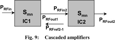
To demonstrate the application of the model to systems with more than one IC, two op-amps were cascaded with pin 6 (output) of IC1 connected to pin 3 (input) of IC2 as shown by Figure 9. The test set-up used two SMD microwave test jigs. The interconnection used was a short length of semi-rigid cable. The device circuit was designed as a non-inverting buffer.
S
mnS
mn PRFin
PRFout1
IC1 IC2
PRFin2
[image:4.595.87.288.148.280.2]PRFout2 PRFref2-1
Fig. 9: Cascaded amplifiers
For the cascaded amplifier measurement the RF signal exits from pin 6 (output pin) IC1 through the semi-rigid
cable and is injected into pin 3 (non-inverting input pin) of device IC2.
The sub-circuit model can be implemented in PSpice using a double circuit schematic, based on Figure 6, and simulated using PSpice. The individual measured S-parameters of the ICs were used to build the PSpice model. The measured results (Figure 10) for the cascaded op-amps show close agreement between the
[image:4.595.316.521.173.324.2]PSpice simulation and the measurement S21 .
Fig. 10: PSpice simulation and measured results for propagation of interference in two cascaded op-amp
circuits via a single path.
The model can also demonstrate the effect of more than one RF propagation path. Again, two amplifiers were connected in cascade with pin 6 (output) and pin 7 (positive power pin) of IC2 connected to pin 3 (non-inverting input) and pin 7 of the device designated IC3 as shown by Figure 11. The test set-up used two SMD
microwave test jigs as described before. The
interconnections used were two lengths of semi-rigid cable.
Smn Smn
HF
PRFin pin3 PRFout pin6
IC2 PRFin pin7 IC3 PRfout pin6
PRFout pin7
PRFfin pin3
Fig. 11: Multi-path RF propagation in cascaded amplifiers
The RF signal was injected into device designated IC3 via pin 6 (output pin) and pin 7 (positive power rail pin) of IC2 into pin 3 (non-inverting input pin) and pin 7 (positive power rail pin) of ic3. The sub-circuit model can be implemented in PSpice using a double circuit schematic including the multiple pin configurations, based on Figure 6, and simulated using PSpice.
The results (Figure 12), show close agreement between
the PSpice simulation and the measurement S21 for
[image:4.595.312.513.470.543.2] [image:4.595.83.285.590.660.2]Fig. 12: PSpice simulation of coupling against measured coupling for multiple propagation paths
(2) in the two-op-amp cascade.
THE NON-LINEAR SUBSYSTEM
Voff(n, f, Vint)
Vn(f)
Voffn
Amplifier
Where Voff(n, f, Vint) is non-linear
equation
andnindicates the node for RF injection
[image:5.595.85.279.295.368.2]LF Signal + VII
Fig. 13 The Non linear subsystem, the Low Frequency component
Figure 13 shows the voltage offset sub-system used to describe the non-linear behaviour of the circuits in the presence of sinusoidal interference.
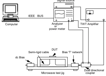
Non-linear parameter measurement
Computer Analyzer TWT Amplifier Signal source
Microwave test jig DUT
Bias 'T' network Semi-rigid cable
dc Bias
FP RP
or power meter
1 2
IEEE BUS
[image:5.595.100.278.499.627.2]Dual directional coupler
Fig. 14: Non-linear measurement block diagram Figure 14 shows the test set up to the measure the device’s non-linear characteristics; this shows the use of a dual directional coupler and dual power meter for measuring injected powers. This set-up in conjunction
with a dedicated software routine allows the net RF power delivered to the device under test to be measured and be recorded to a file. The test procedure for non-linear susceptibility of the device is as follows: a single test frequency (100MHz to >6GHz) is selected and the drive power to the TWT amplifier is slowly increased. The voltage offset, measured at pin 6 (output pin), is continuously monitored at the output of the device using a voltmeter connected to the DC bias pin of the Bias ‘T’ as the forward power is increased. The forward incident
wave voltage Vmeasurement can also be used instead
of power levels, same set-up method as discussed, using the directional coupler. This will provide two different methods to model the non-linear effects on the device.
Non-linear Results
Figure 15 shows the voltage offset measured at pin 6 of the device due to the non-linear effects of the RF signal injected into pin 3 (non-inverting input pin). The device used for this part of the work was the LM308 Super Gain Operational Amplifier which was tested on the DIL component test jig. Five devices from the same batch of components were tested for susceptibility.
Using the susceptibility data and using a Trendline Polynomial fit routine it is found that:
netpower K
netpower K
VoutRF 1 2 2 (5)
where K1 and K2 are constants as a function of
frequency.
Another method to measure the susceptibility against net power is to use the Forward Voltage at node1 of Figure 3, instead of net power, to derive the non-linear
equations. The Forward Voltage V has an advantage
over net power in that it will be easier to use in PSpice and also numerical modelling routines.
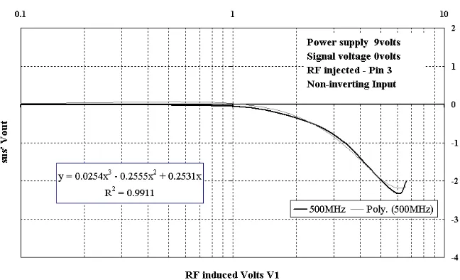
Using the results from equation (3) the Forward Voltage
V can be used as the RFI drive voltage in the
simulation of the model. This was carried out using the TL061 Operational Amplifier and the result is shown in Figure 16. Using the susceptibility data and using a Trendline Polynomial fit routine it is found that:
V K V K V K
VoutRF 33 22 1 (6)
where K1, K2 and K3 are constants as a function of
frequency.
SUMMARY AND CONCLUSIONS
the model uses a linear S-parameter to represent a subcircuit that describes the radio frequency propagation through the device. This is illustrated by Figures 10 and 12 and shows close agreement between the calculated and measured data.
a non-linear frequency dependent function to
generate offset voltages that are injected into the LF part of the model. Simple polynomial functions (Figures 15 and 16) have been devised, from measurements, to give the correct response on the device from the frequency and power levels of the injected RF.
The method described here could be developed to model the propagation and effect of EMI in systems whether analogue or digital.
Work has been carried out on IC immunity
measurements to look at standardisation of RF power levels to upset criteria [9]. The linear propagation model might be used just as a go/no-go detector comparing the power levels from PSpice simulation to this upset criterion for the device i.e., is the RF level on this pin above a susceptibility threshold for upset.
The linear subsystem could be simply interfaced to numerical electromagnetic models to determine it’s level of susceptibility due to interference from external electromagnetic fields. Numerical electromagnetic tools can be used to determine the induced voltages sources
on and s-parameters of PCB tracks and
interconnections. These can be combined with the device models to predict interference levels at any node in a system.
REFERENCES
[1] James J. Whalen, “Predicting RFI Effects in
Semiconductor Devices at Frequencies above 100MHz” IEEE Transactions on Electromagnetic Compatibility, Vol.EMC-21, No.4, pp. 281-282, November 1979.
[2] R E. Richardson Jr, “Modeling of microwave
rectification RFI effects in low frequency circuitry”. Rec. IEEE 1978 Internat. Symb. Electromagn. Compat. (IEEE pub. 78-CH-1304-5 EMC), pp. 71-76, June 20-22, 1978.
[3] Joseph G. Tront, James J. Whalen, Curtis E,
Larson, and James M. Roe, “Computer-Aided
Analysis of RFI Effects in Operational Amplifiers”
IEEE Transactions on Electromagnetic
Compatibility, Vol.EMC-21, No.4, pp. 297-306, November 1979.
[4] James J. Whalen, Joseph G. Tront, Curtis E,
Larson, and James M. Roe, “Computer-Aided
Analysis of RFI Effects in Digital Integrated
Circuits” IEEE Transactions on Electromagnetic Compatibility, Vol.EMC-21, No.4, pp. 291-297, November 1979.
[5] J F. Dawson, J. Wood, W. Persyn, and S. Hagiwara, “The need for Macro-models in the Simulation of EMI Effects in Integrated Circuits”, EMC'94 ROMA, Rome, 13-16 Sept 1994, pp 638-643
[6] J F. Dawson, S. Hagiwara, “Simulation of
Electromagnetic Interference in Integrated Circuits using the SPICE Circuit Modeling Package”, IEE Colloquium: "Electromagnetic Hazards to Active
Electronic Components", Savoy Place, London,
14th January 1994, Digest Number 1994/008, pp 1/1-1
[7] PSpice. Microsim Corporation, Irvine, USA.
http://www.microsim.com
[8] John S. Gerig, “Create S-Parameter Subcircuits for
Microwave and RF Applications”, Wideband
Associates, MicroSim Application Notes,
MicroSim Corporation, California
[9] European Aircraft EMC Research Group.
© British Crown Copyright 1999 / DERA
Published with the permission of the controller of Her
Susceptibility of a LM308N chip [designated 3] amplifier at 500MHz Super Gain Operational Amplifier
y = -97.297x2+ 43.925x - 5 R2= 0.9958 y = -87.438x2+ 45.4x + 1
R2= 0.9978
-9 -7 -5 -3 -1 1 3 5 7 9
1.00E-06 1.00E-05 1.00E-04 1.00E-03 1.00E-02 1.00E-01 1.00E+00
net power W
chip3 -5volt
chip3 1volt
Poly. (chip3 -5volt)
[image:7.595.115.483.118.299.2]Poly. (chip3 1volt) Power supply 9volts Signal voltage -5volts Signal voltage +1volt RF injected -Non-inverting Input
Fig. 15: Comparing measured offset voltages and the polynomial approximation of offset voltage with input power at 500MHz.
[image:7.595.113.437.362.559.2]