1
Prognostic System for Power Modules in Converter Systems Using Structure
Function
Attahir Murtala Aliyu, Alberto Castellazzi
Power Electronics, Machines and Control (PEMC) Group, University of Nottingham, United Kingdom
Email: [email protected]
Tel: +44 / (0) – 1159515568, Fax: +44 / (0) – 1159513764
Abstract
This paper proposes an on-board methodology for monitoring the health of power converter modules in drive
systems, using vector control heating and structure function to check for degradation. It puts forward a system
that is used on-board to measure the cooling curve and derive the structure function during idle times for
maintenance purposes.The structure function is good tool for tracking the magnitude and location of degradation
in power modules. The ability to keep regular track of the actual degradation level of the modules enables the
adoption of preventive maintenance, reducing or even eliminating altogether the appearance of failures during
operation, significantly improving the availability of the power devices. The novelty in this work is the complete
system that is used to achieve degradation monitoring; combining the heating technique and the measurement
without additional power components except the measurement circuit which can be integrated into the gate drive
board and the challenges encountered. Experimental results obtained from this show that it is possible to
implement an on-board health monitoring system in converters which measures the degradation on power
2
1.
Introduction
The need for increased power density in power electronics has led to the invaluable requirement of reliability and
health studies as devices are exposed to harsher environment. Power converters that use insulated gate bipolar
transistors (IGBT) modules are becoming more common in automotive, rail-traction, aerospace, renewable
energy and several other applications where the combination of environmental and load-derived thermal cycling
can result in large and unpredictable fluctuations in junction temperature [1]. An example of this is power
converters used in airborne applications to drive electrical actuators in the close vicinity of the jet engine. In this
case, the power devices are required to survive at the same time static environment temperatures of about 200°C
during the flight and extreme thermal cycles between -55°C and 200°C with a rate of 10°C/min during landing
and take-off [2]. Automotive, rail and wind converters also experience large temperature variations. In traction
application (rail, automotive), during operation the semiconductor device induces a temperature field inside the
IGBT module, which evolves depending on the speed along a railway-service commercial line (mission profile).
Consequently, the power module experiences several local thermal cycles defined by the train acceleration and
braking processes [3]. In wind applications the temperature variation is also dependent on the operating conditions
and the unpredictable variation in the wind speed [4].
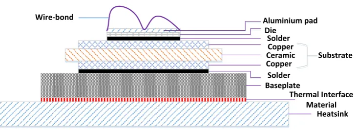
The power module is made up of different layers and several materials. This is designed to provide mechanical
stability, electrical insulation and thermal conductivity[5]. The conventional power module is usually made up
of eight layers and the wire bond as seen in Fig. 1. Table. 1 enumerates the different materials used layer by layer,
their varying thickness and the coefficients of thermal expansion. The coefficient of thermal expansion indicates
change of a component’s size with a change in temperature. Specifically, it measures the fractional change in size
per degree change in temperature at a constant pressure. As the temperature of the power module increases and
decreases the different materials expand and contract at different rates; this induces stress in layers between the
different materials. A major reason for failures in IGBT modules is mismatched coefficients of expansion (CTE)
of the layers an IGBT consists of. The main failure mechanisms are wire-bond cracking, wire-bond lift off , solder
joint fatigue ,solder voids, aluminzation [2]. Fig. 2 shows some of the main failure mechanisms, wire-bond lift
off, solder fatigue and solder voids. With the rise of improved wire-bond technologies and diffusion soldering or
sintering as die attach, it was found that solder fatigue of the substrate-to-baseplate interface rather than wire
bond lift-off is the limiting reliability factor [6, 7]. It has also been presented in [5] that in the substrate-baseplate
3
dimensions are present. Hence the focus in this work is on the degradation that occurs in the solder layer betweenthe substrate and the baseplate.
Aluminium pad Die
Solder
CeramicCopper Copper
Solder Baseplate
Substrate
Thermal Interface Material
[image:3.595.118.484.136.269.2]Heatsink Wire-bond
[image:3.595.185.414.354.654.2]Fig. 1. Illustration of Conventional Power Module Cross Section
Table. 1. Power Module Materials, Thickness and CTE
No Material Thickness
(μm)
CTE ppm/°C
1 Aluminium
(Al)
300 ~22
2 Silicon (Si) 250 ~3
3 Solder 100 -
4 Copper (Cu) 280 -
5 Al2O3 or AlN or
Si3N4
1000 ~7/4/3.3
6 Copper (Cu) 280 -
7 Solder 180 -
8 Cu or AlSiC 4000 ~17/8
Fig. 2 (Left) Wire-Bond Lift Off (Right) Solder Fatigue and Solder Voids
The failure mechanisms need to be detected in order to prevent abrupt destruction of the devices. Therefore to
detect the impending failure, cursor/cursors of detecting the failure mechanisms need to be defined. Some
4
parameters related to the device or device structure will be related to the failure mechanisms. The thermalresponse function (cooling or heating curve) as a result of power step excitation contains information of structure
of the device. Hence by measuring the thermal response function a change in the structure can be detected. The
junction temperature then is an important parameter to monitor degradation; the power modules are enclosed and
provide no opportunity for a direct measurement of the junction temperature. The state of the art methods to obtain
the junction temperature include the integration of NTC resistors[8], on –chip diodes[9] and the use of the thermal
sensitive electric parameter (TSEP). Both NTC and on-chip diodes require special consideration during design
and manufacturing process to ensure electrical isolation from HV traces on the substrate and require additional
external pins and separate copper traces, which might increase manufacturing cost and give rise to new reliability
issues [10].
In the absence of direct measurement, TSEP is a reliable way of measuring the junction temperature. These
parameters are collector emitter voltage (Vce), threshold voltage (Vge(th)), gate resistance (RG), and the turn off
time. The collector emitter voltage [11-14], threshold voltage [15], gate resistance [16], turn off time[17] all have
a defined dependence on temperature and are therefore called temperature sensitive electric parameters (TSEP).
The temperature measured from the TSEP is used to derive the thermal transient and thermal impedance. The
choice of the TSEP depends on the application and the several criteria presented [18]:
• Temperature sensitivity; TSEPs have different values of temperature sensitivity, a greater TSEP temperature
sensitivity gives better measurement results
• Measurement error; the influence of non-thermal effects during measurement is different for each TSEP
• Linearity; the linear relation between TSEP and temperature is a desired property, which is not always full filled
• Repeatability; there should be no large scattering of TSEP values between different samples.
The choice of TSEP is in this work is based on the fact that the aim is to measure the dynamic temperature of the
device. Therefore a continuous measurement of the temperature is needed. This eliminates the use of the threshold
voltage, turn-off time as regular switching is needed in order to obtain the temperature. The Vce as presented in
[19], exhibits the characteristics mentioned above such as high repeatability, linearity. The sensitivity of this TSEP
depends on the current levels as can be noticed from the relationship between current, voltage and temperature in
the IV curves (see Fig. 22 ). In this work, since the measurement is to be carried out at low currents the sensitivity
5
Prognostic real-time systems in [20, 21] present a method that uses compact thermal models to predicttemperatures of inaccessible locations of a power module; the information obtained is then combined with data
about the reliability analysis to predict failure mechanisms. Although those methods might be able to predict
failure, it gives an estimate, hence doesn’t provide the actual variation in the quantity of the failure mechanism.
Also as time elapses the aging of the power modules will affect the integrity of the thermal model. Adaptive
models for real-time monitoring have been presented in [10, 22-25], which compares physical measurement with
a model estimate to accurately track the junction temperature of the device under consideration. The limitations
of [10, 22, 23] are that the collector emitter voltage is noisy and intermittent due to the non-linearity of the I-V
characteristic of the IGBT, hence this method is dependent on the operating region. [24] requires extending the
turn-on time by making modifications to the gate drive in order to measure the temperature online. In [25]
temperature sensors need to be embedded in the baseplate to detect the change in temperature distribution, this
method is affected by the positioning of the sensors.
As opposed to the real-time monitoring solutions, which take measurements of the TSEP of the device during
operation of the inverter, in the methodology proposed here, measurements are taken when the system is not
operation(during maintenance routines).The in-situ method in [26] to which this work mainly makes reference
to, works by injecting external currents into the power module during idle times. The high current is injected
externally to heat the devices. However, in [26] a set of relays need to be inserted to select which device undergoes
test, with severe limitation of the applicability of such solution and considerable complication of the testing
methodology. The method in [27] presents a similar control concept of a quasi-real-time prognostic method in
simulation , however in practice this will also be subject to noisy and intermittent collector emitter voltage which
makes it hard to implement.
The methodology used here provides a system that uses the structure function[28] to measure degradation
on-board without making changes to the connections, making use of additional components or dismounting it; it is
also able to point out if and where degradation occurred in the structure of the device. An original approach in
this paper is the implementation of a test routine (on-board) which can be carried out between operational phases
of the equipment, such as in trains once a week/month in the depot for maintenance routines using vector control.
The two aspects to obtaining the structure function are, heating the power device and measurement. In Section 2,
6
function and how it can be obtained. In Section 3, the heating methodology which makes use of vector control isalso elaborated. In Section 4 the amalgamation of the heating and measurement system with the challenges
encountered are presented along with the results validating the on board measurement methodology
2.
Degradation Monitoring Methodology
Measuring thermal transients is a typical method for thermal characterisation of semi-conductor device packages.
The method itself is essentially the recording of the thermal response function of the structure for step function
excitation [28]. This means that the cooling and heating curves contain information about the power
semi-conductor device packages structure
2.1 Thermal Impedance extraction
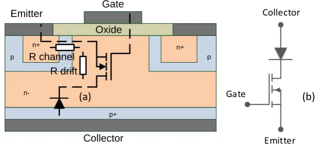
As mentioned earlier, the collector-emitter voltage (Vce) is used to measure the temperature of the IGBT. An
N-channel IGBT can be considered as an N-Channel MOSFET on a p type substrate; this is shown in Fig. 3(a). The
p-n junction at the collector forms a diode; hence, the equivalent circuit of an IGBT can be represented by Fig.
3(b).
Emitter
Collector Oxide Gate
R channel R drift
p+
n-p p
n+ n+
Collector
Gate
[image:6.595.150.457.445.588.2]Emitter
Fig. 3. IGBT Structure & Equivalent Circuit
The p-n junction features a well-known temperature dependence on its on-state voltage[13]. This dependence can
be used to calibrate the device at different temperatures by using a constant low bias current to prevent self-heating
of the IGBT. The characteristic of the MOSFET begins to come into effect after the knee voltage of the diode has
been surpassed. After the knee voltage, the voltage drop due to the channel resistance (Rchannel) and drift resistance
(Rdrift) dominate.
7
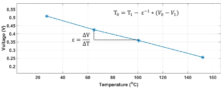
Although the I-V characteristic of a modern IGBT chip exhibits a positive temperature coefficient at nominalcurrent levels, i.e. Vce increases with increasing temperature for a constant injected current; the temperature
coefficient is generally negative for low currents. In this current regime Vce decreases almost linearly with growing
temperature at a rate ε of approximately -2mV/K [13]. Therefore a linear relationship for a Magna Chip
[image:7.595.114.484.194.339.2]MPMB75B120RH is created by measuring the Vce at different reference temperatures as it can be seen in Fig. 4.
Fig. 4. Temperature Dependence of Vce for a sense current I=100mA (Magna Chip MPMB75B120RH)
In order to obtain the figure shown above, the calibration process needs to be carried out. The calibration process
is carried out on a hot plate or oven that has the ability to provide different fixed temperature levels. A fixed
temperature is needed in order to ensure homogeneity of temperature at the chip; meaning the whole module is
held at a constant temperature.
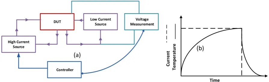
The Vce then, can be used to obtain the cooling curve of the IGBT. A basic method of measuring the cooling curve
is, passing a constant high current through the device under test to heat up the device using a high current source.
A switch is placed in the high current path to turn on and off the high current during heating and measurement
respectively. The switch is controlled by control platform; the controller provides interrupt to start the
measurement of the cooling curve. The voltage measurement is connected to the controller through a data
acquisition assistant (DAQ). When the interrupt is received, the DAQ acquires the cooling curve measurement.
During the measurement the constant low current used for calibration passes through the device to create a voltage
drop proportional to temperature. This relationship is obtained from the device calibration mentioned earlier. The
measurement system is shown in Fig. 5(a). Also an illustration of the resulting heating current pulse and the
temperature profile are presented in Fig. 5(b).
ε =ΔV ΔT
8
ControllerHigh Current Source
DUT Low Current
[image:8.595.71.519.72.209.2]Source Voltage Measurement C u rr e n t Te m p e ra tu re Time
Fig. 5.(a) Cooling Curve Measurement Chart (b) Illustration of Heating Current Pulse & Temperature Profile
2.2 Structure Function
The thermal impedance contains information about the power semi-conductor device packages structure. The
thermal impedance is derived from the cooling curve by equation (2). The structure function which is then derived
from the thermal impedance is a graphical representation of the device structure that makes use of the thermal
models (Foster and Cauer). The structure functions are obtained by direct mathematical transformations from the
heating or cooling curves [29].The schematic shown in Fig. 6 shows the process involved in obtaining the structure
function. The thermal transient measurement (cooling) is affected by noise, therefore proper filtering needs to be
applied in other to make use of the thermal transient curve for further processing. In this work, the filtering
technique used is a numerical average of every point on the thermal transient. This carried out by obtaining
multiple thermal transients from the system to ensure that no information regarding the thermal transient is altered
during filtration. The filtered curve is obtained using equation (1). Where T is the average temperature at a certain
time instance, t is the total duration of the thermal transient (or last time instance/point), n is the number of curves
to be averaged and a,b,c are the temperatures at a certain time instance, for a single measured curve.
n i i t n i i n i ifiltered
T
n
a
T
n
b
T
n
c
Temp
1 1 2 1 11
...
,...
1
,
1
( 1 )
After filtering the thermal transient curve, the next step is calculating the thermal impedance curve from the
thermal transient using equation (2).
T
(
t
)
t
Z
th( 2 )
9
Fig. 6.Schematic Process of Obtaining the Structure Function.The cooling curve can be described by in the simplest form by the response function of a single time constant
system. It has the mathematical form of
[28]:
e
T
t
a
(
)
*
t( 3 )
If a single exponential represents a simple function response as in equation (3), for a more complex thermal
structure it can be considered as an infinite sum of the individual exponential terms with different time constants
and magnitudes.
n i t ith
T
e
Z
1(
0
)
*
( 4 )
From this equation if the thermal impedance curve is obtained (which can be derived from the thermal transient
curve) then the thermal resistances and capacitances can be obtained from the time constants (τ=R*C). There are
several methods of achieving this, the graphical method, curve fitting and deconvolution [28, 30]. The obtained
thermal resistances and capacitances make up the Foster network. As mentioned earlier the Foster network does
not have any relation to the physical structure. Therefore the Foster network derived from the thermal transient
has to be converted to a Cauer type network. The synthesis of passive networks is used to convert the Foster
network to Cauer Network. The thermal capacitances can be calculated from the heat source to the heat sink by
considering an equation of the input impedance of the Foster network in Laplace form. The method was shown in
[31] where the impedance and the admittance are both used to achieve the goal. This method is shown below
n
i
1
...
( 5 )Y
C
s
s
Z
i i i
)
(
1
( 6 )
Z
R
s
Y
i i i1
)
(
1
( 7 )Where Zn+1=0
This process is carried out for the number of times equal to the capacitor and resistors in the foster network. From
10
C
R
s
R
C
R
s
R
s
Z
i i i i i i in 1 1 11
1
)
(
( 8 )This can be re-arranged as:
R
C
R
C
s
R
R
C
C
s
R
R
C
R
R
C
R
R
s
s
Z
i i i i i i i i i i i i i i i i in 1 1 2 1 1 1 1 1 11
)
(
( 9 )To begin the process equation (9) should be inverted so its format matches equation (6). This provides the
capability to obtain the first thermal capacitance in the Cauer network using factorisation. The remainder is then
inverted to conform to equation (7), as a result of which the corresponding thermal resistance is obtained.
The structure function uses the thermal resistances and capacitances in the cauer form (because Cauer networks
have a link with the physical structure) to identify changes in the devices structure. The advantage of the structure
function is that it does not only reveal the value but also the location of the thermal resistance and capacitance in
the heat flow path. There are two types of structure function, differential and cumulative.
2.2.1 Cumulative Structure Function
The cumulative structure function is also known as the Protonotarios-Wing function[33]. This is a function that
presents a graphical representation of the structure of the device by using the thermal capacitance and thermal
resistance. The cumulative structure function is sum of the thermal capacitances CΣ (cumulative thermal
capacitance) in the function of the sum of the thermal resistances RΣ (cumulative thermal resistance) of the
thermal system, measured from the point of excitation towards the ambient. Discretization of the structure function
results in a Cauer network. As pointed in Fig. 7 each slice represents a corresponding Cauer thermal capacitance
and resistance.
………
………
…
11
Fig. 7. Cumulative Structure Function and Relationship to Cauer NetworkWhere Rthn and Cthn :
11 1 in thi n
i thi
thn
R
R
R
( 10 )
11 1 ni thi n
i thi
thn
C
C
C
( 11 )The X-axis which is the thermal resistance is representative of the depth of the device because thermal resistance
is proportional to the thickness. The thermal capacitance is on the Y-axis and the sudden transition means change
from one material to another.
2.2.2 Differential Structure Function
In [34] the differential structure function is defined as the derivative of the cumulative thermal capacitance with
respect to the cumulative thermal resistance, by
R
d
C
d
R
K
)
(
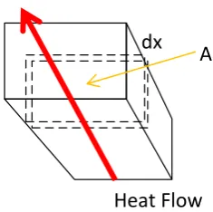
( 12 )Fig. 8. One Dimensional Heat Flow Model
Considering a dx wide slice of a single matter of cross section A, we can calculate this value. Since for this case
dCΣ=cAdx, and the resistance is dRΣ=dx/λA, where c is the volumetric heat capacitance, λ is the thermal
conductivity and A is the cross sectional area of the heat flow, the K value of the differential structure function is
A
c
A
dx
cAdx
R
K
(
)
2
( 13 )
A
dx
Heat Flow
[image:11.595.234.352.467.584.2]12
Fig. 9. Differential Structure FunctionThis value is proportional to the c and λ material parameters, and to the square of the cross sectional area of the
heat flow, consequently it is related to the structure of the system. In other words: this function provides a map of
the square of the heat current-flow cross section area as a function of the cumulative resistance. In these functions
as shown in Fig. 9 the local peaks indicate reaching new surfaces (materials) in the heat flow path, and their
distance on the horizontal axis gives the partial thermal resistances between these surfaces. More precisely the
peaks point usually to the middle of any new region where both the areas, perpendicular to the heat flow and the
[image:12.595.144.453.585.733.2]material are uniform
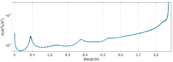
Fig. 10. Acoustic scan of test diodes solder layer
The differential structure function was used to check the difference in the solder layer between the two test diodes
in Fig. 10. In Fig. 11(a) the shift in thermal resistance between the well soldered (solid-blue) and the badly soldered
(dash-orange) diodes is noticed at a thermal resistance of less than 0.1W/K. This indicates the difference occurs
in the die region.
(a) Good solder
Bad solder
Die
reg
io
n
Su
b
str
ate
reg
io
13
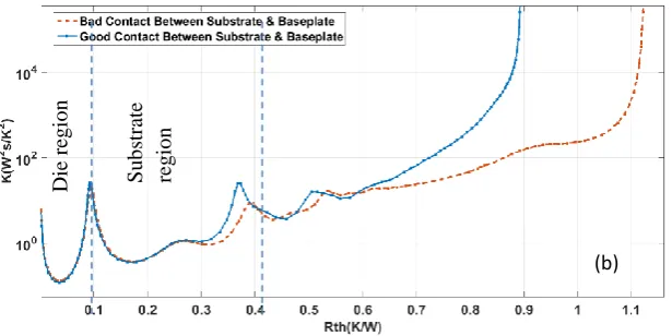
Fig. 11.Differential structure function of the (a) solder layer (no-voids and voids) (b) same device withdifference at the substrate
While in Fig. 11(b) measuring the same diode but changing the force of contact at the bottom of the substrate
shows a difference at a higher thermal resistance; which is directly proportional to depth. This indicates that not
only the change in thermal resistance can be obtained but its location.
3.
Heating Methodology
A three phase 2-level inverter is used in this work as case study. One important aspect of obtaining the cooling
curve is the heating current. In this study, the DC supply voltage of the inverter will be used to supply the heating
current while attached to an induction motor because tests need to be on-board and carried out during
non-operational periods. Therefore the induction motor needs to be stationary while heating the IGBTs and diodes.
The vector control is used because it provides the opportunity to control the torque current (isq) and field current
(isd) independently similar to DC machines. Thus the rotation of the machine can be prevented by applying a zero
torque producing current and then the field current will be injected to heat up the devices. These conditions make
it suitable for maintenance routine. To elaborate this, consider the rotor equation in the q plane and applying a
zero speed as rotor needs to be stationary. The result is
𝟎 =𝒅𝝋𝒓𝒒 𝒅𝒕 +
𝑹𝒓 𝑳𝒓𝝋𝒓𝒒−
𝑳𝒐
𝑳𝒓𝑹𝒓𝒊𝒔𝒒
(14) Whereir,Rr, Rs, φr, φsLo,Lr, are the rotor current, stator and rotor resistances, fluxes, magnetizing inductance, and rotor inductance respectively. Using rotor flux orientation, the rotor flux φr (yellow) is positioned on the d axis shown in Fig. 12. This means that the rotor flux has no q component (φrq=0) as seen in Fig. 12. Therefore equation (14) can be written as:
(b)
Die
reg
io
n
Su
b
str
ate
reg
io
14
−𝑳𝒐
𝑳𝒓𝑹𝒓𝒊𝒔𝒒= 𝟎 , isq=0 (15)
α β
d Rotor flux axis q
Rotor axis φr
ωe
[image:14.595.167.403.92.242.2]is
Fig. 12 Rotor flux orientation
This means to achieve zero speed isq should be 0 as shown in equation (15). Considering the rotor equation in the
d plane with the same conditions as above the result is:
𝑖𝑠𝑑 = ( 𝑑𝜑𝑟𝑑 𝑑𝑡 +
𝑅𝑟
𝐿𝑟𝜑𝑟𝑑 )/( 𝐿𝑜
𝐿𝑟𝑅𝑟) (16)
Defining the Magnetising current im as: 𝜑𝑟𝑑 = 𝐿𝑜𝑖𝑚
𝒊𝒔𝒅=𝑹𝑳𝒓 𝒓
𝒅𝒊𝒎
𝒅𝒕 + 𝒊𝒎 (17) At steady state isd = im. Hence in rotor flux orientation isq is defined as the torque current and isd is defined as the
field producing current. Therefore applying zero torque current isq and a certain fixed value for the magnetizing
isd was carried out experimentally using indirect rotor flux orientation (IRFO) to heat up the devices. A detailed
explanation of this process can be found in a previous work [35].
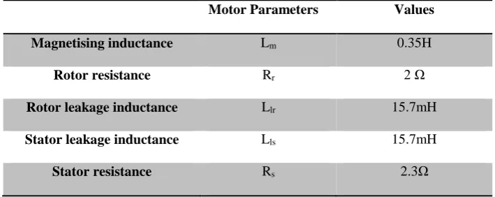
Table. 2: Motor parameters
Motor Parameters Values
Magnetising inductance Lm 0.35H
Rotor resistance Rr 2 Ω
Rotor leakage inductance Llr 15.7mH
Stator leakage inductance Lls 15.7mH
[image:14.595.120.475.605.746.2]15
The parameters of induction machines are very important when considering advanced control techniques likevector control. The two procedures used to extract induction motor parameters presented in table 2, are to test the
motor under no-load and locked rotor conditions. With the parameters it is possible to calculate the control
parameters shown in Fig. 13. The PI controllers for the isd and isq current are identical. Using the isq=0A as
derived from the equations above and the isd reference as 7A in vector control using indirect rotor flux orientation
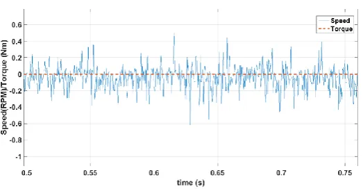
shown in Fig. 13, zero speed (see Fig. 15) of the motor is achieved while still being able to heat the devices. The
isd feedback and reference is shown in Fig. 14(a). The output currents are shown in Fig. 14(b), the current in phase
A is 7A and the other currents in phase B and C are -3.5A, hence a balanced condition. The resulting speed and
torque of the motor indicating that the system (for example train) is stationary is presented in Fig. 15.
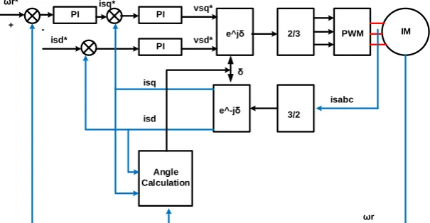
IM PWM 2/3
3/2 e^jδ
e^-jδ PI
PI PI
Angle Calculation
ωr δ
isabc
ωr* isq*
isd*
vsq*
vsd*
isd isq
+
-Fig. 13. Block diagram of vector control (IRFO)
[image:15.595.150.453.287.444.2]16
Fig. 14. (a) isd current and reference (b) Phase currentsFig. 15.Speed and torque of induction motor during heating
4.
Application of Degradation Monitoring in Inverter Set-up
The overall test setup and measurement system are shown in Fig. 16 (a) and (b) respectively. The measurement
circuit is shown on the right. It contains of two parts; measurement board and the isolation board. On the supply
side of the converter 200V DC was applied and a switching frequency of 10 KHz. Vector control is applied with
an isd reference of 7A to the inverter in order to heat up the devices as stated earlier. After reaching a steady
temperature all the switches in the converter are turned off except the switch that its junction temperature is to be
measured. This is done to ensure there is no current flow from the supply side during the measurement. The
measurement circuit and the three phase current sensors are connected to the analog-to-digital converter (A/D) on
the FPGA. An encoder also provides a speed feedback to the FPGA. It is important to note that this process can
be carried out without the use of an encoder by directly entering the isq reference. But in order to ensure safe
[image:16.595.169.431.230.366.2]17
Fig. 16.Inverter set-up and measurement circuitThe steps used to measure the voltage across the IGBT are highlighted in Fig. 17. The first step is the ability to
measure a small voltage drop across the IGBT in the existence of high DC link voltage. The next step is signal
conditioning, to improve the resolution of the signal by adding a gain and an off set. Hence utilizing the full range
of the A/D used to acquire the data in the FPGA. After these processes an isolation circuit is used to provide the
FPGA galvanic isolation from high power.
Fig. 17. Measurement process
The measurement circuitry is based on the work in [11]. Two diodes D1 and D2 shown in Fig. 18 are connected
in series and a current source forward-biases them during the IGBT on time. When the IGBT is off, the D1 diode
is blocking the Vce voltage, protecting the measurement circuitry from damage. Assuming the two diodes are
identical (VD1 = VD2), the Vce voltage may be measured by subtracting the voltage drop on diode D2 from the
Vb potential. This mathematical function can be realized using the circuit shown in Fig. 18.
𝑽𝒄𝒆= 𝑽𝒃− 𝑽𝑫𝟐= 𝑽𝒃− (𝑽𝒂− 𝑽𝒃) = 𝟐𝑽𝒃− 𝑽𝒂 ( 18 )
The circuit in Fig. 18 makes it possible to implement the equation above. The first op-amp (highlighted in red)
does the mathematical function of producing 2Vb in (18). The second part (highlighted in green) of the circuit
completes the mathematic function using a differential amplifier to obtain Vce (2𝑉𝑏− 𝑉𝑎). This op-amp can have another function of setting a gain to utilize the A/D range.
Converter
FPGA
Measurement
circuit
circuit
Gate drives
Isolation
board
Measurement
board
Measurement
Circuitry
Signal
Conditioning
[image:17.595.85.486.370.469.2]18
Fig. 18 .Schematic of measurement circuit .Reprinted from [11]After the heating period, the cooling curve needs to be measured by passing the low current used to calibrate the
device. This is carried out as mentioned earlier by switching on S1 and the others off as shown in Fig. 19. Due to
the energy stored in the motor inductance current free wheels through the devices switched on for measurement
and the top 2 diodes in the 2 other phases as shown in Fig. 19. This means that the low current measurement
cannot be carried out during the free-wheeling period due to high current flowing in the device intended for
measurement in this period. A voltage (collector-emitter) and current measurement of the device was carried out
at this stage and it can be seen in Fig. 20 that the current decays slowly.
DC
S1 S2 S3
S4 S5 S6
L1 L2 L3
Device ON
Device OFF
Fig. 19. Inverter during Measurement Phase
From Fig. 20, it can be observed that it takes approximately 0.8 seconds for the current to reach the level of the
measurement current. If the measurement is to start at 0.8 seconds most information of the structure of the device
will be lost as the die, solder and substrate faster time constants. The data sheet gives information about the
[image:18.595.170.421.423.623.2]19
matching this information to the derived normalized temperature (divided by the power dissipation) shown in Fig.21, the approximate time constant from the junction to the case can be obtained. In this case, the obtained time
constant from the graph is 0.2512 seconds. This means that any measurement that starts past this time constant
[image:19.595.143.453.176.335.2]contains information only of the heat sink. Therefore any degradation present in the device will not be recorded.
Fig. 20.Current and Voltage (collector-emitter) of DUT
Fig. 21. Normalized Temperature Curve
To solve this problem the methodology will be outlined. Since the current stored in the inductor flows through the
device and the voltage is always measured. The collector current against the collector emitter voltage (I-V curves)
at different temperatures can be used to measure the temperature by creating a look-up table. These curves were
derived using the curve tracer. In Fig. 22 the measured device IV line is the measured voltage and current passing
through the device. However this curve passes through a point on the I-V curves where there is no difference in
voltage and current for all the temperatures. This means that it is impossible to measure at this point (inflexion
point). But above and below this point the sensitivity gradually decreases. The highlighted area in Fig. 22 below ∆t=0.793
[image:19.595.177.442.375.509.2]20
the inflexion point has a lower sensitivity (to noise) of about 2mV/°C and the highlighted area above this regionhas a higher sensitivity (to noise) of 0.9mV/°C. By considering the equation
𝑉 = 𝐿𝑑𝑖𝑑𝑡 ( 19 )
The options present in order to increase di/dt are to reduce the inductance or increase the voltage. To reduce the
inductance is impractical. To increase the voltage is possible but limited by the system design. The other option
is increase di/dt by controlling the current in order to exploit the point below the inflexion point. One of the reasons
for this is that the region has a lower sensitivity (to noise) and also it is known that there is negligible self-heating
[image:20.595.127.472.288.546.2]in this region as the current is low.
Fig. 22. I-V Curves and Measured Device current and Voltage
Results
The methodology used to solve this problem is to use the controller (vector control), which was used to heat the
devices to force the current, to a low value so that the region in the I-V curves will be of a low sensitivity. It can
be seen in Fig. 23 that the reference changes from 7A to a low value (0.2A in this case). The current changes faster
(from 7A to 0.2A in 2ms) than in the previous case. This means that the self-heating is negligible, also, faster time
constants will be recorded. In this case the measurement starts when the current falls below 1A as it can be seen
from Fig. 22. The sensitivity of the IV curves reduces as the current approaches zero therefore less error in the
measurement. The junction temperature measurement is shown in Fig. 24 which starts at 4ms the due to initial
Sensitivity range ≈2mV/°C Inflexion Point
Sensitivity range ≈0.9mV/°C
21
temperature variations. It is imperative to obtain the fastest time constant possible, measuring much slower than4ms will mean that the time constant for the solder between the substrate and the heat sink cannot be measured.
Two curves are presented here to show that this process is repeatable and reliable. This is important because the
whole process is done to check for degradation in power modules. The structure function [9, 10] is used to process
these curves. The structure function is used as it provides a comprehensive graphical representation of what is
[image:21.595.144.451.220.382.2]going on in the device. The structure function of the two measured cooling curves can be seen in Fig. 25.
Fig. 23. Current and Voltage During Measurement Using Vector Control.
[image:21.595.151.445.434.582.2]22
Fig. 25 Differential structure function showing repeatability of this processThis methodology is used to check for degradation in the MPMB75B120RH Magna Chip module. The module
was power cycled using constant current technique with a current of 52A on a dedicated power cycling equipment.
An on time 50s and an off time of 60 seconds is used (45.45% duty cycle). The minimum junction temperature
and the maximum junction temperature can be seen in Fig. 26. The minimum junction temperature during cycling
is 6°C and the maximum junction temperature is 137°C before initiation of degradation process. Degradation can
be seen in the maximum junction temperature curve after 8000 cycles. This is also the case with the ∆Tj because
the minimum junction temperature is constant. The initial ∆Tj before degradation shown in Fig. 27, was chosen
in order to accelerate the cycling process. The maximum ∆Tj is chosen that will not exceed device maximum
operating temperature by choosing the appropriate cycling current and duty cycle.
[image:22.595.149.446.489.636.2]23
Fig. 27. ∆T showing Degradation starting after 8000 cyclesBefore the cycling process started initial tests were carried out for the sake of comparison. An acoustic scan of
the power device solder layer between the substrate and baseplate was carried out as can be seen in Fig. 28(a).
The differential structure function of the power device was also measured. The differential structure function was
validated with the datasheet. Structure function measurements were carried out at the beginning; a film was placed
between the baseplate and the heatsink in one measurement, and the other measurement with no film. The
differential structure function can be seen in Fig. 29(a). The typical junction to case temperature according to the
data sheet is 0.25, this matches the differential structure function as the difference starts to occur at that thermal
resistance value on the structure function. After the degradation was observed by the acoustic scan in Fig. 28(b)
the shift in thermal resistance indicating degradation can be seen in earlier peaks indicating degradation in the
solder layer in Fig. 29(b). This means that with this methodology the structure function of the power devices can
be measured to indicate degradation
Fig. 28. (a) Scanning Acoustic Microscope at time 0 (b) After 10000 cycles
(a)
(b)
[image:23.595.175.421.492.577.2]24
Fig. 29. Differential structure function (a) before cycling with the same module and including a film betweenbaseplate & heat-sink (b) comparing initial measurement with no film to measurement after cycling
5.
Conclusion
This work has shown that degradation in power modules can be measured using the structure function. The ability
to detect the region where degradation occurred has also been shown by intentionally inducing degradation
between the substrate and the baseplate. The on-board heating technique with vector control using indirect flux
rotor orientation to make the induction motor stationary while passing current through the switches in the power
module in order to obtain thermal transients has also been shown experimentally. This gives rise to the means of
checking the health of power modules regularly on-board without additional high current sources to prevent
unforeseen failures during operation. As vector control is used for the heating; the existing software only needs a
simple modification. The measurement circuit can also be included on the gate driver board.
Difference due to film occurs here
Difference due to degradation occurs here
(a)
25
6.