Silicon spin diffusion transistor: materials, physics
and device characteristics
C.L. Dennis, C.V. Tiusan, J.F. Gregg, G.J. Ensell and S.M. Thompson
Abstract: The realisation that everyday electronics has ignored the spin of the carrier in favour of its charge is the foundation of the field of spintronics. Starting with simple two-terminal devices based on giant magnetoresistance and tunnel magnetoresistance, the technology has advanced to consider three-terminal devices that aim to combine spin sensitivity with a high current gain and a large current output. These devices require both efficient spin injection and semiconductor fabrication. In the paper, a discussion is presented of the design, operation and characteristics of the only spin transistor that has yielded a current gain greater than one in combination with reasonable output currents.
1 Introduction
Everyday electronic devices manipulate carriers solely based on their charge, either positive or negative. Their operation ignores the fact that those carriers also have a spin, either spin up or spin down. Spintronics aims to remedy this deficiency by manipulating the spin as well as the charge of the carrier in nanoscale devices. Spintronics goes beyond the simple use of magnetic fields to alter the movement of charge, as in the Hall effect. Instead, spintronics determines and/or senses the spin orientation of the carriers by incorporating magnetic materials into conventional devices. Spins injected into a material are polarised either optically or by passing through a magnetic material, which polarises the carriers parallel (or antiparallel depending on the material) to the direction of magnetisation. The difference in behaviour of carriers of different spin types only becomes apparent when they travel through a magnetic material. For example, when spin-up electrons are injected into a magnetic material with the net magnetisation pointing in the same direction, these spins pass through relatively unscathed. However, spin-down electrons are heavily scattered. This leads to different conductivities (resistivities) for the different spin types. It is upon this principle that most of the suggested devices are based.
This field has expanded rapidly in recent years. It was only a few years from the discovery of giant magneto-resistance (GMR) [1]to the first commercial production of a GMR-based read head for a disk drive (by IBM in 1997). Recent research has focused on expanding the
scope of spintronics from two-terminal to three-terminal devices. This has led to the development of a number of different three-terminal designs [2–9] (which will be briefly discussed in Section 2) that aim to exploit the spin-dependent scattering of charge carriers to yield a device with high current gain and high magnetic sensitivity. This paper will focus on the silicon-based spin diffusion transistor, the only spin transistor which yields a current gain greater than one. The discussion will begin with the fabrication, followed by the experimental results. It will conclude with a discussion of how the fabrication and materials affect the output characteristics.
2 General operating principles of spin transistors
2.1
Johnson transistor
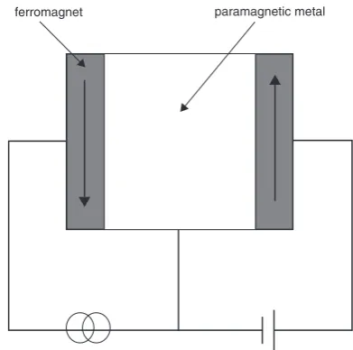
The first spin transistor was the Johnson bipolar transistor
[2], which added a third terminal connection to the nonmagnetic spacer layer in a CPP-GMR trilayer (see Fig. 1). Bipolar has double meaning: positive and negative charge carriers, up- and down-spin carriers, and output which is either a positive or negative current/voltage. This spin transistor device requires that the thickness of the layers be comparable to or smaller than the spin diffusion length of the material.
paramagnetic metal ferromagnet
Fig. 1 Schematic of the Johnson bipolar transistor C.L. Dennis and J.F. Gregg are with the Clarendon Laboratory, Parks Road,
Oxford OX1 3PU, UK
C.V. Tiusan is with the Laboratoire de Physique des Materiaux, Facult!e des
Sciences, Universit!e H. Poincar!e, Nancy 1, Boulevard des Aiguillettes B.P. 239
54506 Vandoeuvre les Nancy, France
G.J. Ensell is with the Department of Electronics, University of Southampton, Southampton SO17 1BJ, UK
S.M. Thompson is with the Department of Physics, University of York, York, YO10 5DD, UK
E-mail: [email protected]
rIEE, 2005
IEE Proceedingsonline no. 20050008
doi:10.1049/ip-cds:20050008
[image:1.595.330.526.562.756.2]As the electrical characteristics of this purely ohmic device are magnetically tunable, it can potentially be used as a field sensor or as nonvolatile magnetic random access memory. However, owing to its all-metal construction, its operation yields only small voltage output changes and no power or current gain (power gain may be possible in 5-terminal (as opposed to a 3-terminal) architecture). If such a device could generate a current gain, it could potentially be used to make logic devices[10].
2.2
Monsma transistor
The next step was to try and incorporate semiconductors with magnetism to further expand the field of spintronics by generating novel functionality. The Monsma transistor[3], produced at the University of Twente, was the first hybrid spintronic device (see Fig. 2). (The Mizushima MIFS transistor[4]is a second variant on this design, where one of the Schottky barriers is replaced by a tunnel barrier.) First fabricated in 1995, it sandwiched a CPP-GMR multilayer between two semiconductors (silicon). Schottky barriers form at the interfaces between the silicon and the metal structure and these absorb the bias voltages applied between pairs of terminals. The collector Schottky barrier is back-biased and the emitter Schottky is forward-biased. This injects (unpolarised) hot electrons from the semicon-ductor emitter into the metallic base high above its Fermi energy. If the hot electrons travel across the thickness of the base and retain enough energy to surmount the collector Schottky barrier, then they will exit through the collector; otherwise, they will exit via the base.
emitter base
base collector
emitter
collector e
ε
Fig. 2 Schematic of the Monsma transistor (from[3])
fermi level φ
fermi level M
1
2
3
4 IE
IC
emitter
base
collector
M Al2O3
VEB VBC
CoFe
GaAs(111) CoFe
eVEB
A
Fig. 3 Schematic of the magnetic tunnel transistor (from[5])
VG
VG Schottky
InGaAs 2DEG InAlAs
gate
analyser z
z y
y x 45°
polariser
electro-optic material
a
b
z y 45°
iron contact
iron contact
Fig. 4 Schematic of the spin FET (from[7])
2qζ
Eg
n emitter n collector
IE IB
p base Vbi− VBC Vbi− VBE
IC
Fig. 5 Schematic of the magnetic bipolar transistor (from[8])
E
E EF
EF
h
h M M
d1 d
2
V2
V3
J J V1
d3
−h
−h 2h
2h o
FM emitter
FM collector SC
base
I I
n-up
n-down
o n-up
n-down
Fig. 6 Band structure of the spin diffusion transistor
emitter 65×65 µm2
15×15 µm2
65×65 µm2 22 µm n- or p-type Si (3 ± 0.5µm)
Al (1µm) Si wafer (525µm) Si wafer (525µm)
Si3N4 (2−3nm)
SiO2 (500nm) SiO2 (600nm) base
doped Si (177nm)
Co (30nm) collector
Fig. 7 Structural schematic diagram of the fabricated spin diffusion transistor with silicon base
[image:2.595.325.529.37.243.2]By varying the magnetic configuration of the base magnetic multilayer the operator can determine how much energy the hot electrons lose in their passage across the base. If the magnetic layers are antiferromagnetically aligned in the multilayer, then both spin types experience heavy scattering in one of the magnetic layer orientations, so the average energy of both spin types as a function of distance into the base follows an exponential decay curve. On the other hand, if the magnetic multilayer is in an applied field and its layers are all aligned, one spin type gets scattered heavily in every magnetic layer, whereas the other travels through the structure relatively unscathed. It may thus be seen that, for parallel magnetic alignment, spins with higher average energy impinge on the collector barrier and the collected current is correspondingly higher.
However, one limiting factor of this device is that it only used the semiconductor to control the distribution of applied potentials across the device; it is the metallic components that are spin selective. Despite this, the Monsma transistor represents a very important step in the evolution of spintronics. It has electrical characteristics that are magnetically tunable, plus a current gain and magnetic sensitivity that are sufficiently large so that, with help from some conventional electronics, it is a candidate for a practical working device. However, to release the full potential of hybrid spintronics, the devices need to exploit spin-dependent transport in the semiconductor itself.
2.3
Magnetic tunnel transistor (MTT)
The next generation of spin transistor devices modified the Monsma transistor by incorporating the knowledge gained from the theoretical analysis of spin injection. The Schottky barriers were replaced by tunnel barriers to form the magnetic tunnel transistor[5]. This device (shown in Fig. 3) is fabricated by depositing a magnetic tunnel junction on top of a GaAs substrate. The first ferromagnet acts as the emitter, the second ferromagnet as the base, and the
semiconductor acts as the collector. The device works by injecting spin-polarised electrons across the tunnel barrier from the first ferromagnet into the second ferromagnet. The voltage applied between the emitter and collector is dropped across the tunnel barrier, thereby controlling the amount of current that reaches the base (the second ferromagnet). If the base is thin enough, then the current reaching the base will travel ballistically across the base and have enough energy to surmount the Schottky barrier between the second ferromagnetic metal and the semiconductor. (The ferromagnet/insulator/ferromagnet/insulator/metal (FIFIM) transistor by Ounadjela and Hehn[6]is a variant on this, where the Schottky barrier is replaced by another tunnel junction.) Any electrons that do not have enough energy will be swept out the base as a base current. The magnetic sensitivity again derives from the differential scattering of hot electrons of different spin types in the second magnetic layer. The sensitivity is dramatically ‘amplified’ by the exponential spin-energy decay; inciden-tally, this latter feature makes the magnetic trilayer structure on the left of the device a very effective spin polariser. However, it is again the metallic components that determine the magnetic sensitivity.
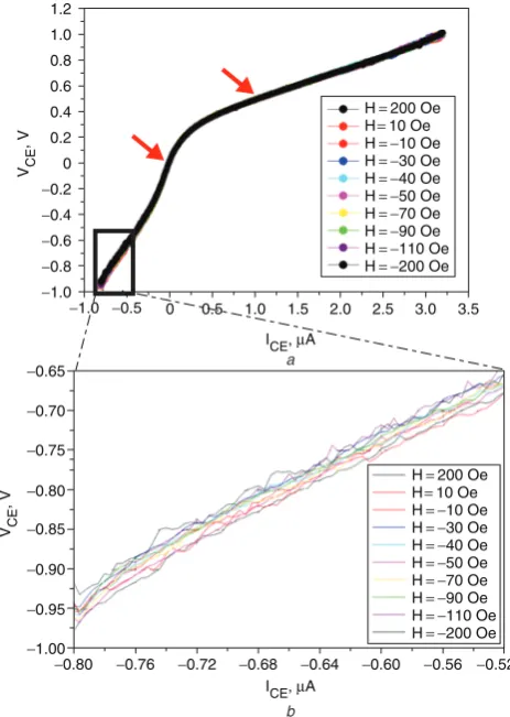
VCB
IB
IE VL
RL
VCE
VCE ICB
ICE
IC B
B
B C
C
C
E E
E
a
c
b
+
Fig. 8 Measurement circuit for the collector to base circuit, the collector to emitter circuit, and common-collector configuration The collector, base and emitter are labelled C, B and E, respectively. The grey arrows indicate sign conventions for positive current. A black single arrow indicates that the magnetic layer on that contact is fixed, whereas the black double arrows indicate that the magnetisation of that contact is free. The + andsigns indicate the polarity of the applied voltage. Note that the sign conventions are the same regardless of whether the Si base is p-type or n-type
aCollector to base circuit bCollector to emitter circuit cCommon-collector configuration
0.8 0.3 −0.2 −0.7 −1.2 −1.7 −2.2 −2.7 −3.3
−3.5 −3.0 −2.5 −2.0 −1.5 −1.0 −0.5 0 0.5 1.0
−1.0 −0.8−0.6 −0.4−0.2 0
hopping conduction regime Fowler-Nordheim tunnelling regime fit to data
hopping conduction regime Fowler-Nordheim tunnelling regime fit to data
0.2 0.4 0.6 0.8 1.0 1.2 VCB, V
a
b
−1.0−0.8−0.6 −0.4 −0.2 0 0.2 0.4 0.6 0.8 1.0 VCE, V
ICB
,
µ
A
ICE
,
µ
A
Fig. 9 Two-terminal characteristics of the p-type transistor The dots indicate measured data points (where black dots indicate the region where Fowler–Nordheim tunnelling dominates and blue dots indicate the region where hopping conduction dominates) and the solid red lines are the fits, according to the regime the data is in a V–I curve for p-type spin transistor (II-6): collector to base, four regimes and their fits
[image:3.595.311.544.298.674.2]2.4
Spin field-effect transistor (spin-FET)
A fourth transistor was developed in parallel with the previous devices: the experimental realisation of a spin-FET (see Fig. 4) based on the proposal by Datta and Das[7]in 1990. This transistor is a modification of a field-effect transistor (FET), where an applied electric field changes the width of the depletion region and, hence, its electrical resistance. In a spin FET, spin-polarised electrons are injected from a magnetic source into a semiconductor channel. During passage through the channel, these electrons undergo Rashba precession, the frequency of which depends on the gate voltage. Finally, the electrons are analysed by spin selective scattering in the magnetic drain. Hence, the actual electrical characteristics are dependent on, not only the magnetic orientation of the source and drain, but also on the gate voltage. Gardelis and co-workers[11]have made a step towards realising this device, but the gate functionality remains to be demonstrated. It may be noted that the characteristics of the spin FET differ from those of the device in the following subsection in that its gmmay be a
periodic function of gate voltage and may change sign on application of a magnetic field.
2.5
Magnetic bipolar transistor (MBT)
This fifth variant, which is analogous to an ordinary bipolar junction transistor (BJT), has been explored theoretically in
[8, 9]. Like the spin FET, the magnetic bipolar transistor (see Fig. 5) has not yet been realised experimentally, although a prototype has been fabricated [12]. Like the BJT, this device consists of two p–n (n–p) junctions connected in series and operates in a similar manner. The active (current amplification) region occurs under the same conditions for both devices: the emitter-base junction is forward-biased and the base-collector junction is reverse-biased. However, in the MBT, the emitter and collector are nonmagnetic, but the base is magnetic, creating spin-split conduction bands (see Fig. 5). It may also have a spin-polarised injector. As the conduction band in the base has a spin splitting 2qz, the electrons that flow from emitter to base are spin polarised. As such, the emitter efficiency is dependent on the number of electrons available to flow into the base. Hence, the current amplificationb¼DIC/DIBcan
be controlled, not only by the spin polarisation in the base, but also by the nonequilibrium spin in the emitter. This additional dependence of b in an MBT is called [9]
magnetoamplification. −1.0
−0.2 −0.1 −0.1 −0.1 0
−0.9 −0.8 −0.7 −0.6 −0.5 −0.4 −0.3 −0.2 VCB, V
−1.0 −0.8 −0.6 0 0.2 0.4 0.6 0.8 1.0 −0.5
0.5 1.0 1.5 2.0
0
−0.4 −0.2 VCE, V
a
b ICB
,
µ
A
ICE
,
µ
A
hopping conduction regime Fowler-Nordheim tunnelling regime fit to data
[image:4.595.312.548.26.417.2]hopping conduction regime Fowler-Nordheim tunnelling regime fit to data
Fig. 10 Two-terminal characteristics of the n-type transistor The black dots indicate measured data points (where black dots indicate the region where Fowler–Nordheim tunnelling dominates and blue dots indicate the region where hopping conduction dominates) and the solid red lines are the fits, according to the regime the data is in aV–I curves for n-type spin transistor (II-8): collector to base, four regimes and their fits
bV–I curve for n-type spin transistor (II-8): collector to emitter, four regimes and their fits
5 4 3 2 1 0
Ic
,
µ
A
Ic
,
µ
A
−1
−2 IB=−1.0 µA
IB=−1.0 µA IB= 1.0 µA
IB= 1.0 µA
−1.0 −0.8 −0.6 −0.4 −0.2 0 0.2 0.4 0.6 0.8 1.0
a
−1.0 −3.5 −3.0 −2.5 −1.5 −2.0 −1.0 −0.5 0.5 1.0 1.5
0
−0.8 −0.6 −0.4 −0.2 0 0.2 0.4 0.6 0.8 1.0 VEC, V
VEC, V
b
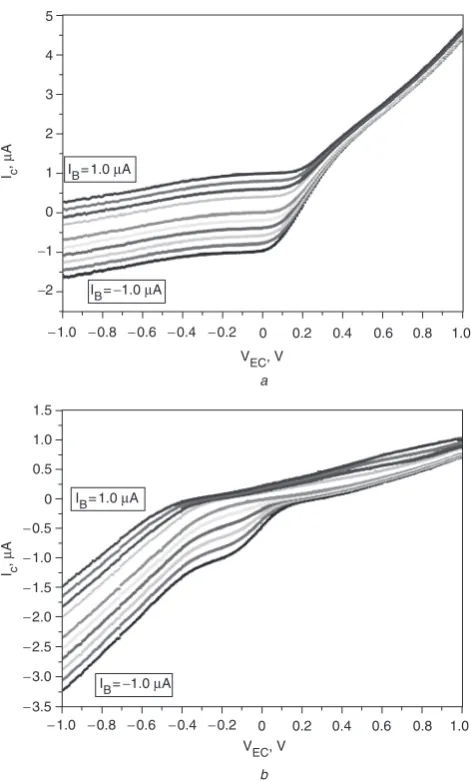
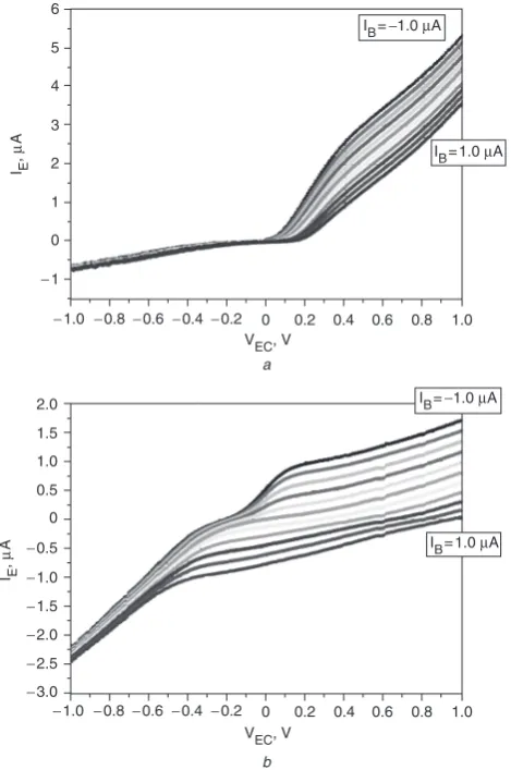
Fig. 11 IC–VEC characteristics of spin diffusion transistors in
common-collector configuration and zero applied field
The load resistor RL¼9976O. The step size of IBis 0.2mA with the starting and ending currents as indicated in the boxes
a Common collector configuration of p-type Southampton spin transistor (II-6), H¼0 Oe, RL¼9.976 kO
[image:4.595.50.284.29.398.2]3 General operating principles of spin diffusion transistor
In the preceding Section, we summarised the state of the art in three-terminal spintronics. These devices comprised both all-metal and hybrid metal-semiconductor transistors. The fabricated devices all have a common feature, namely that the spin selectivity/spin transport is limited to the metallic components of the device. In this paper, we discuss a different design, which is distinguished by two main features. First, the semiconductor does more than simply control the distribution of applied voltages; the operation of the device depends on spin transport within the semi-conductor itself. Secondly, it is the only spin transistor design capable of current gains equal to or in excess of unity (against other spin transistors which have a current gain of less than 103). Reference [13] illustrates why this low current gain is the main sticking point for industrial applications, as well as some of their other limitations. In the remainder of the paper, we discuss the fabrication and characterisation of this new spin diffusion transistor.
The basic operation of this device is similar to a bipolar junction transistor (although it is most closely related to the classical tunnel transistor [14, 15]). This spin diffusion transistor injects a spin-polarised current from the emitter
into the electric-field-screened base region. The current which diffuses across the base is driven primarily by a carrier concentration gradient, which forces the carriers injected by the emitter to wander towards the base along the top of an extended energy barrier, at the bottom of which lies the collector. This energy barrier is also spin-selective (according to the magnetic orientation of the collector) and determines if these polarised carriers are allowed to fall into the collector or not. Thus, we have a device with a respectable current gain from which power gain may be derived, but whose characteristics may be switched by manipulating the spin selectivity of the energy barrier via an externally applied magnetic field. In this particular device (see Fig. 6), tunnel barriers are used to provide the electric-field shielding of the semiconductor base. However, as outlined in [16], a wide variety of designs are possible in principle, including variants that use p–n junctions, Schottky barriers or spin tunnel junctions.
−1.0 −1
0 1 2 3 4 5 6
−0.8−0.6−0.4−0.2 0 0.2 0.4 0.6 0.8 1.0
a
b
VEC, V
−1.0 −0.8−0.6 −0.4−0.2 0 0.2 0.4 0.6 0.8 1.0 VEC, V
IB=−1.0 µA
IE
,
µ
A
IE
,
µ
A
−3.0 −2.5 −1.5 −2.0 −1.0 −0.5 0.5 1.0 2.0 1.5
0
IB= 1.0 µA IB= 1.0 µA
[image:5.595.51.286.30.384.2]IB=−1.0 µA
Fig. 12 IEVEC characteristics of spin diffusion transistors in
common-collector configuration and zero applied field
Load resistor RL¼9985O. The step size of IB is 0.2mA with the starting and ending currents as indicated in the boxes
a Common collector configuration of p-type Southamptom spin transistor (II-6), H¼0 Oe, RL¼9.985 kO
b Common collector configuration of n-type Southamptom spin transistor (II-8), H¼0 Oe, RL¼9.985 kO
−1.0 0 0.2 0.4 0.6
βC
,
µ
A
βC
,
µ
A
0.8 1.0 1.2
0 0.2 0.4 0.6 0.8 1.0
−0.8 −0.6 −0.4 −0.2 0 0.2 0.4 0.6 0.8 1.0 VEC, V
a
−1.0 −0.8 −0.6 −0.4 −0.2 0 0.2 0.4 0.6 0.8 1.0 VEC, V
b
IB=−1.0 µA
IB=−1.0 µA
IB= 1.0 µA
[image:5.595.314.544.32.408.2]IB= 1.0 µA
Fig. 13 Calculated current gain at zero field as a function of emitter-collector voltage
For p-type and n-type spin diffusion transistors in zero applied magnetic field. The step size of IB is 0.2mA with the starting and ending currents as indicated in the boxes. The current gain is determined by calculating the change in collector current for change in base current and was done between adjacent pairs of base currents (as shown in the legend) at all voltages
aCollector current gain of p-type Southampton spin transistor (II-6) in common collector configuration: H¼0 Oe; RL¼9.976 kO
4 First generation of spin diffusion transistors
4.1
Processing
The samples were fabricated using standard photolithogra-phy on n- and p-type silicon-on-insulator (SOI) wafers with a measured resistivity of 2–1000O-cm. The details of the process are specified in [17, 18], so only the relevant aspects are provided here. The base contacts were heavily doped to form ohmic contacts. Tunnel barriers of Si3N4were deposited on the collector and emitter contacts
by low-pressure epitaxy. Then, all three contacts had 30 nm of Co and 1mm of Al (for the electrical contacts) deposited by sputtering. The resulting structure is shown in Fig. 7.
4.2
Electrical characteristics in zero applied
magnetic field
This device has been examined in detail in[17, 18], the main points are only summarised here for comparison with the second generation.
4.2.1 Two-terminal I–V characteristics
: TheI–V characteristics of the collector-to-emitter (CE) circuit and the collector-to-base (CB) circuit were performed at room temperature in the circuit configurations shown in Figs. 8aandb. Typical results are shown in Figs. 9 and 10, and differ slightly between the two types of transistors, although the overall form is the same in both. As shown previously [17, 18], these tunnel barriers conduct at low voltages (oB0.5 V) by Mott’s variable range hopping conduction[19, 20], and at higher voltages (4B0.5 V) by Fowler–Nordheim tunnelling [21]. The existence of two different conduction methods is significant, because it has been well-established experimentally [22] that hopping conduction destroys the spin polarisation of carriers (as the time it takes to hop from one state to the next can exceed the spin lifetime of the carrier). Hence, no magnetic sensitivity should be observed in the hopping conduction regime.
4.2.2 Three-terminal I–V characteristics
: Whenconnected in common collector configuration (see Fig. 8c), the transistor exhibits similar characteristics (see Figs. 11, 12) to that of a conventional bipolar
transistor: a dependence on both the base current and the emitter-collector voltage. However, the difference in the I–V characteristics between the n- and p-type transistors can be explained by either different doping in the silicon resulting in different minority carriers traversing the base or electron domination of the tunnelling process (due to the difference in effective masses for electrons and holes), causing one device to be a majority carrier device and the other to be a minority carrier device.
The emitter current as a function of base current and emitter-collector voltage is as high as1.56mA (3.09mA) for p-type (n-type) spin diffusion transistor, which occurs at
VEC¼ 1 V and IB¼ 1.0mA. Not only is this a higher output current than in the metal-based devices (by 3 orders of magnitude), but it also occurs at a lower voltage. At a slightly higher base current of 0.6mA (see Fig. 13), the current gain (b) is 1.0370.03 (0.9670.03) for p-type (n-type). At a base current of 0.8mA, the current gain (b) is 1.0670.05 for the p-type transistor. Furthermore, the
1.2
0.8
0.4
0
normalised magnetic response
−0.4
−0.8
−1.2
1.2
0.8
0.4
0
normalised magnetic response
−0.4
−0.8
−1.2
−250−200−150−100 −50 0 50 100 150 200 250 applied magnetic field, Oe
a
b
[image:6.595.52.281.29.197.2]−250−200−150−100 −50 0 50 100 150 200 250 applied magnetic field, Oe
Fig. 15 Normalised magnetic response minus Si background of spin diffusion transistors
Owing to shape anisotropy, the collector switches atB7307Oe and the emitter and base at B71157Oe. This means that the magnetic moments of the emitter and collector Co layers are parallel for applied magnetic fields from –115 Oe to +30 Oe and greater than +115 Oe, and are antiparallel for positive applied magnetic fields between 30 Oe and 115 Oe
ap-type spin diffusion transistor bn-type spin diffusion transistor
−0.2 0.2 0.4 0.6 0.8 1.0 1.2 1.4
n-type
p-type
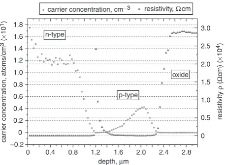
oxide 1.6
carr
ier concentr
ation, atoms/cm
3 (
×
10
1)
resistivity
ρ
(
Ω
cm) (
×
10
4)
resistivity, Ωcm 1.8
0 0
0.5
0.4 0.8 1.2 1.6 2.0 2.4 2.8 depth, µm
carrier concentration, cm−3
0
1.0 1.5 2.0 2.5 3.0
Fig. 14 Spreading resistance data for p-type spin diffusion transistor
[image:6.595.310.547.33.433.2]transfer ratio (a¼IE/IC) is calculated to be one within error
for positive and negative VEC, for both the p-type and
n-type transistor at IB¼0mA. This means that all of the
emitter current is being transferred into the collector current. Hence, as the current gain is not identically equal to 1, the base current must be modifying either the amount of recombination in the Si, or the current injected into the Si from the emitter.
The transistor action is due solely to the presence of the silicon, because it occurs at any and all applied magnetic fields, and not to any spin transport in the silicon. It depends on a nonequilibrium condition (a surplus of minority carriers) being established at the first tunnel barrier, and continuing to the second barrier. In an ideal bipolar (tunnel) transistor, these minority carriers would diffuse across the base, as almost all of the applied voltage would be dropped over the depletion region of the p–n junctions (the tunnel barriers). However, this device does not have a uniform field in the base, resulting in a position dependence of the base minority carrier density. This is supported by the spreading resistance data (see Fig. 14), which indicate a nonuniform doping profile as well as a weak p–n junction in the silicon base. This inhomogeneity manifests itself as a parasitic resistance of 200 kO(980 kO) for the p-type (n-type) transistor. The presence of this
parasitic base resistance limits the total output current and the current gain; in particular, the tunnel barrier ceases to dominate the output current at B0.4 V (B0 V). This corresponds with the IV characteristics, which are a straight line above 0.4 V (B0 V) for the p-type (n-type) device, as well as with the location of the decrease in the current gain.
4.3
Electrical characteristics in an applied
magnetic field
The magnetic response of the Co layers in the spin diffusion transistors was measured using a vibrating sample magnet-ometer (VSM). These hysteresis loops (see Fig. 15) indicate that differential switching is occurring in the devices, where the collector contact switches at the lower field ofB7307Oe, and the emitter and base switch at the higher field of
B71157Oe. Application of a magnetic field is expected to affect the I–V characteristics in two ways. First, the magnetisation of the emitter and collector Co contacts can be differentially manipulated, thereby introducing a spin-selective tunnelling magnetoresistance (TMR) effect that modulates the collector current. Secondly, the applied magnetic field decreases the mean free path in the silicon base via Lorentz magnetoresistance [23] (LMR) thereby
1.0 0.8 0.6 0.4 0.2 0 −0.2 −0.4 −0.6 −0.8 −1.0 −1.2
−4 −3 −2 −1 0
ICB, µA
a
b
ICB, µA
VCB
, V
VCB
, V
1
3.0 2.9
2.8 2.7
2.6 0.84 0.86
0.88 H = −500 H = −220 H = −130 H = −115 H = −100 H = −90 H = −80 H = −70 H = −60
0.90 0.92 0.94
[image:7.595.50.284.26.396.2]2 3
Fig. 16 Two-terminal characteristics of p-type spin diffusion transistor as a function of applied magnetic field from collector to base
Note the ‘activity’ (oscillations) around the coercive fields. (These samples were saturated at positive fields.)
a Full V–I curve where the arrows show the onset of Fowler– Nordheim tunnelling
bBlow-up of the highlighted regions inato show the detail
1.0 0.8 0.6 0.4
V CE
, V
V CE
, V
0.2 0 −0.2 −0.4
−5 −4 −3 −2 −1 0 1
ICE, µA
a
b
1.05 1.00 0.95 0.90 0.85 0.80 0.75 0.70 0.65
0.5 0.6 0.7
ICE, µA
0.8 0.9 −0.6
−0.8 −1.0
H =100 G H =10 G H = 00 G H =−50 G H =−75 G H =−150 G
[image:7.595.315.542.26.408.2]H =100 G H =10 G H = 00 G H =−50 G H =−75 G H =−150 G
Fig. 17 Two-terminal characteristics of p-type spin diffusion transistor as a function of applied magnetic field from collector to emitter
a Full V–I curve where the red arrows show the onset of Fowler– Nordheim tunnelling
also affecting the collector current. Both of these are observed in these devices.
4.3.1 Two-terminal magnetic I–V
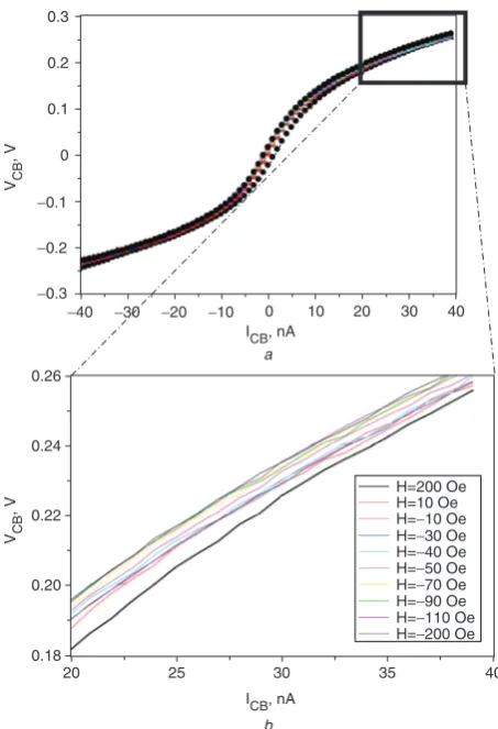
character-istics
: The two-terminal measurements of Section 4.2.1 were repeated with a magnetic field applied in the plane of the transistor (perpendicular to the current). There are three important results (see Figs. 16–20) in these measurements. First, the I–V characteristics are a function of applied magnetic field. Secondly, no magnetic sensitivity is observed for voltages below the onset of Fowler–Nordheim tunnel-ling. This concurs with the claim that hopping conduction is occurring at low voltages. Thirdly, most of the ‘activity’ (shown in the inset of Figs. 16–20 as the ripples or deviations from a straight line) in the electrical character-istics occurs around the magnetic transition region, between90 and115 Oe. This suggests that the deviations may be due to magnetic domain formation and/or motion in the Co layers changing the magnetic state seen by different regions of the tunnel barrier.
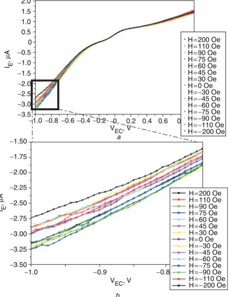
4.3.2 Three-terminal magnetic I–V
character-istics
: The transistor was again operated in common-collector mode with the magnetic field applied in the plane of the transistor (perpendicular to the current). The results in Figs. 21–23 are typical and plot the emitter current as a function of applied emitter-collector voltage and magnetic field at IB¼ 0.6mA. These results show a variation in theemitter current as a function of magnetic field, indicating
that the transistor behaves as a magnetically tunable device with a field-dependent gain. The maximum variation of the average current gain (where b was averaged for all VEC40.4 V and for each base current), relative to the current gain at H¼0 Oe, was1173% (1572%) for p-type (n-p-type) which occurred at 75 Oe (110 Oe) and
IB¼ 0.6mA. On examination of the expanded graphs (see Fig. 24) for both n- and p-type at positive VEC, it is
clear that, when the magnetic moments of the emitter and collector Co layers are parallel, the emitter current is larger than in the antiparallel configuration. (From Fig. 21 it would appear that this magnetic sensitivity occurs in the region where the current gain is small. However, the current gain refers to IC, the collector current and the magnetic
sensitivity plotted in Fig. 18 refers to IEthe emitter current.
Due to BJT definitions of positive current, one is turned ‘on’ in +VEC and the other is turned ‘on’ in VEC.
Therefore, the region of large current gain is the same as the region of large magnetic sensitivity. The emitter current is plotted to show spin injection since the electrons actually flow from the collector to emitter. The same effect is apparent in the collector current due to conservation of charge.)
A detailed analysis of the origins of the magnetic sensitivity is explained in [17, 23], including other possibi-lities besides spin injection (or TMR) such as LMR, anisotropic magnetoresistance (AMR) and fringing fields from the magnetic elements. LMR is definitely measured, while AMR is eliminated, due to the size of the effect, and
0.3 0.2 0.1 0 −0.1 −0.2 −0.3
−40 −30 −20 −10 0
0.26
0.24
0.22
0.20
0.18
20 25 30 35 40
H=200 Oe H=10 Oe H=−10 Oe H=−30 Oe H=−40 Oe H=−50 Oe H=−70 Oe H=−90 Oe H=−110 Oe H=−200 Oe ICB, nA
a
b
ICB, nA
VCB
, V
VCB
, V
[image:8.595.51.278.26.358.2]10 20 30 40
Fig. 18 Two-terminal characteristics of n-type spin diffusion transistor as a function of applied magnetic field from collector to base
Note the ‘activity’ (oscillations) or lack thereof around the coercive fields. (These samples were saturated at positive fields.)
aFull V–I curve
bBlow-up of the highlighted regions inato show the detail
−1.0
−1.0
−0.8
−0.6
−0.4
−0.2
0 0.2 0.4 0.6 0.8 1.0 1.2
−0.5 0 0.5 1.0 1.5 2.0 2.5 3.0 3.5
ICE, µA
VCE
, V
VCE
,V
1.00
0.96
0.92
0.88
0.84
2.68 2.76 2.84 2.92 3.00 3.08
ICE, µA
3.16 a
b
H=200 Oe
H=10 Oe
H= −10 Oe
H= −30 Oe
H= −40 Oe
H= −50 Oe
H= −70 Oe
H= −110 Oe
H= −90 Oe
H= −200 Oe
H=200 Oe
H=10 Oe
H= −10 Oe
H= −30 Oe
H= −40 Oe
H= −50 Oe
H= −70 Oe
H= −90 Oe
H= −110 Oe
[image:8.595.315.546.26.343.2]H= −200 Oe
Fig. 19 Two-terminal characteristics of n-type spin diffusion transistor as function of applied magnetic field from collector to emitter
Note the ‘activity’ (oscillations) or lack thereof around the coercive fields. (These samples were saturated at positive fields.)
a Full V–I curve where the red arrows show the onset of Fowler– Nordheim tunnelling
the Hall Effect from fringe fields is eliminated by symmetry considerations. In particular, the percentage change as a function of field from LMR is 4% of the overall resistance at72007Oe. This is a change ofB40 kO, which originates in part from the parasitic resistance of 200 kO(980 kO) for the p-type (n-type) device.
Assuming the existence of spin injection into Si (as presented in [24]), the spin polarisation can be estimated from Julliere’s model [25] for spin tunnelling to be 2.570.5% for the p-type and 1071% for the n-type (see Fig. 25). This value for the spin polarisation is significantly lower than the theoretical value of 38%, as well as being lower than typical values in the literature. This is to be expected as hopping conduction, though no longer dominant, is still active at high tunnel barrier bias and it destroys part of the injected spin polarisation.
5 Second generation of spin diffusion transistors
5.1
Processing
These samples were identical to the previous generation of devices except in the materials sputtered onto the Si. Tunnelling barriers of Al2O3(1.5 nm) were deposited on the
back of the wafer and tunnelling barriers of Al2O3(1.0 nm)
were deposited on the front of the wafer by sputtering of Al followed by plasma oxidation. Co (3 nm)/Fe (6 nm)/Cu (5 nm)/Cr (3 nm) were deposited on the emitter and base contacts, while CoFe (3–6 nm)/Cu (5 nm)/Cr (3 nm) were
deposited on the collector. The resulting structure is shown in Fig. 26 and an actual device is shown in Fig. 27.
5.2
Electrical characteristics in zero applied
field
5.2.1 Two-terminal I–V characteristics
: I–Vcharacteristics of the collector-to-emitter (CE) circuit and the collector-to-base (CB) circuit were performed at room temperature in the circuit configurations shown in Fig. 8a
and 8b. Typical results on the stable barriers are shown in Fig. 28. However, although these VI characteristics show diode-like behaviour at low bias, they are not accurately represented by the equations for either an ideal diode or a nonideal diode as shown in Fig. 28. Instead, away from zero, the electrical characteristics of the tunnel barriers are linear in voltage and current, and are characterised by a resistance of 300 kO. This resistance is probably also due to the nonuniformity in the Si (as discussed in Section 4.2.2), with additional contributions from diffusion of the oxygen or Al into the surrounding Si, or Co or Fe into the Al2O3.
5.2.2 Three-terminal I–V characteristics
: Asseen in Fig. 29, these results closely resemble the results of the first generation p-type spin diffusion transistors for positive VEC. However, there is negligible conduction in the
negative VEC regime, which results in a collector current
H=200 Oe
H=10 Oe
H= −10 Oe
H= −30 Oe
H= −40 Oe
H= −50 Oe
H= −70 Oe
H= −90 Oe
H= −110 Oe
H= −200 Oe
−0.65
−0.70
−0.75
−0.80
−0.85
−0.90
−0.95
−1.00
−0.80 −0.76 −0.72 −0.68 −0.64 −0.60 −0.56 −0.52
ICE, µA
ICE, µA
VCE
, V
VCE
, V
1.2
1.0
0.8
0.6
0.4
0.2
0
−1.0
−1.0 −0.5 0 0.5 1.0 1.5 2.0 2.5 3.0 3.5
−0.8
−0.6
−0.4
−0.2
a
b
H=200 Oe
H=10 Oe
H= −10 Oe
H= −30 Oe
H= −40 Oe
H= −50 Oe
H= −70 Oe
H= −90 Oe
H= −110 Oe
[image:9.595.50.282.30.356.2]H= −200 Oe
Fig. 20 Two-terminal characteristics of n-type spin diffusion transistor as function of applied magnetic field from collector to emitter
Note the ‘activity’ (oscillations) or lack thereof around the coercive fields. (These samples were saturated at positive fields.)
aFull V–I curve where the red arrows show the onset of Fowler– Nordheim tunnelling
bBlow-up of the highlighted regions inato show the detail
VEC, V VEC, V
IE
, µ
A
I E
,
µ
A
0.80 0.82 0.84 0.86 0.88 0.90 0.92 0.94 0.96 0.981.00 5.4
5.2
5.0
4.8
4.6
4.4
4.2 6
5
4
3
2
1
0
−1.00 −0.75 −0.50 −0.25 0 0.25 0.50 0.75 1.00
H=−200 Oe
H=0 Oe
H=110 Oe H=90 Oe H=75 Oe H=60 Oe H=45 Oe H=−60 Oe H=−75 Oe H=−90 Oe H=−110 Oe
H=−30 Oe H=−45 Oe
H=30 Oe
H=200 Oe
H=−200 Oe
H=−75 Oe H=−90 Oe H=−110 Oe
H=0 Oe H=−60 Oe
H=−30 Oe H=−45 Oe
H=75 Oe H=60 Oe H=45 Oe H=30 Oe
H=110 Oe H=90 Oe
H=200 Oe
a
[image:9.595.313.547.32.376.2]b
Fig. 21 IEcharacteristics as function of applied magnetic field of
p-type spin diffusion transistors in common-collector configuration with IB¼ 0.6mA
The samples were saturated at negative fields aFull V–I characteristics
gain for VECo0 V, identical to 1. Hence, in this range, the
base current does not modify the emitter current (which is zero), it simply adds to it. (For VEC41 V, the current gain plateaued at an average of 0.93370.010. This plateau occurs when the contact resistance begins to exceed the tunnel barrier resistance at a voltage ofB0.9 V.)
5.3
Electrical characteristics in an applied
field
The application of a magnetic field is expected to affect the I–V characteristics in the same ways as in the first generation of spin diffusion transistors. However, the primary expected differences are (i) that the cleaner switching will yield clearer parallel and antiparallel condi-tions and more stable electrical characteristics; (ii) that the larger separation between the coercive fields will yield more distinct parallel and antiparallel conditions and therefore larger TMR values; and (iii) that the new tunnel barriers will conduct spin better leading to a more highly spin-polarised current in the base which will yield greater magnetic sensitivity in the emitter current and larger TMR values.
The magnetic response, as measured by a SQUID Magnetometer, shows three coercivities (see Fig. 30). The base contact switches at HCB10 Oe, the emitter contact
switches at HCB85 Oe, and the collector contact at fields 4100 Oe.
5.3.1 Two-terminal magnetic I–V
character-istics
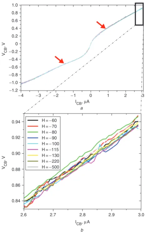
: The two-terminal measurements of Section 5.2.1 were repeated with a magnetic field applied in the plane ofthe transistor (perpendicular to the current). There are three important results (shown in Figs. 31 and 32) from these measurements. First, the I–V characteristics are again a function of applied magnetic field. Secondly, as compared to the two terminal magnetic I–V characteristics of the first generation of devices, the I–V characteristics are much smoother, indicating cleaner magnetic switching than before. Thirdly, the variation in voltage at different applied magnetic fields is as large as 0.0934 V, for the collector to base measurement, and 0.0667 V, for the collector to emitter measurement, which is well outside the error in the measurement of70.0001V (70.1 mV).
5.3.2 Three-terminal magnetic I–V
character-istics
: The transistor was again operated in common-collector mode with the magnetic field applied in the plane of the transistor (perpendicular to the current). The results (see Figs. 33 and 34) show a variation in the emitter current (of up to 0.67270.006mA in 7907Oe) as a function of magnetic field, indicating that the transistor behaves as a magnetically tunable device with a field-dependent emitter gain. The maximum relative variation of the emitter current was1470.3% which occurred at90 Oe, VEC¼1 V andIB¼0.0mA. Overall, the current variation shows a negative
change; the emitter current is being decreased as a function of field.
Close examination of Fig. 34 shows that, although the emitter current for positive VEC varies in an identical
fashion to that expected for TMR-influenced data, there is a field-dependent distribution. Hence, the data do not show a simple TMR/spin injection signature (see Fig. 35): one current for parallel contacts and another for antiparallel H=200 Oe
H=0 Oe H=110 Oe H=90 Oe H=75 Oe H=60 Oe H=45 Oe
H=−60 Oe H=−75 Oe H=−90 Oe H=−110 Oe H=−30 Oe H=−45 Oe H=30 Oe
H=−200 Oe
0.80 0.84 0.88 0.92 0.96 1.00
b
VEC, V
VEC, V
a
1.15
1.10 1.20 1.25 1.30 1.35 1.40 1.45 1.50 1.55
IE
,
µ
A
IE
,
µ
A
−3.5
−1.0−0.8−0.6−0.4−0.2
−3.0
−2.5
−2.0
−1.5
−1.0
−0.5
0 0.5 1.0 1.5 2.0
0 0.2 0.4 0.6 0.8
H=200 Oe H=110 Oe H=90 Oe H=75 Oe
H=0 Oe H=60 Oe H=45 Oe H=30 Oe
H=−60 Oe H=−75 Oe H=−30 Oe H=−45 Oe
[image:10.595.52.286.32.348.2]H=−90 Oe H=−110 Oe H=−200 Oe
Fig. 22 IEcharacteristics as function of applied magnetic field of
n-type spin diffusion transistors in common-collector configuration with IB¼ 0.6mA
The samples were saturated at negative fields aFull V–I characteristics
bBlow-up of the black boxes fromafor detail
−1.0
−3.50
−3.25
−3.00
−2.75
−2.50
−2.25
−2.00
−1.75
−1.50
−0.9
b
VEC, V
VEC, V
a
IE
,
µ
A
IE
,
µ
A
−3.5
−1.0−0.8−0.6−0.4−0.2
−3.0
−2.5
−2.0
−1.5
−1.0
−0.5
0 0.5 1.0 1.5 2.0
0 0.2 0.4 0.6 0
H=200 Oe
H=0 Oe H=110 Oe H=90 Oe H=75 Oe H=60 Oe H=45 Oe
H=−60 Oe H=−75 Oe H=−90 Oe H=−110 Oe H=−30 Oe H=−45 Oe H=30 Oe
H=−200 Oe H=200 Oe
H=0 Oe H=110 Oe H=90 Oe H=75 Oe H=60 Oe H=45 Oe
H=−60 Oe H=−75 Oe H=−90 Oe H=−110 Oe H=−30 Oe H=−45 Oe H=30 Oe
H=−200 Oe
[image:10.595.315.549.33.336.2]−0.8
Fig. 23 IEcharacteristics as function of applied magnetic field of
n-type spin diffusion transistors in common-collector configuration with IB¼ 0.6mA
The samples were saturated at negative fields aFull V–I characteristics
contacts. The two groups have a symmetric contribution, which could be the result of any one of the symmetric contributions discussed in Section 4. Finally, it should be noted that, in both cases, the antiparallel fields yield a larger current than the parallel fields. This is due to Co and CoFe having a different majority spin carrier[26].
By removing these symmetric contributions, the max-imum TMR is calculated (see Fig. 36) to be 13.370.2% at IB¼ 0.2mA. Close examination of the TMR shows their
dependence on the magnetic response of the transistors. At 7307Oe, the base contact has switched. This introduces some spin-polarised current into the Si. (Recall that the base junction here is a tunnel junction and that the base current is predominantly additive, not recombinative.) Although, the emitter contact does not really start to switch until 75 Oe, the magnetisation is dropping slightly. This could lead to the decrease in TMR through 45, 60 and 75, as the
applied magnetic field, Oe
nor
malised magnetisation
−250 −2.68 −2.56 −2.60 −2.64 −2.52 −2.48 −2.44 −2.40 −2.36 −2.32
−200−150−100 −50 0 50 100 150 200 250 IB= −0.6 µA
applied magnetic field, Oe magnetisation
−250−200−150−100 −50 0 50 100 150 200 250
IE
,
µ
AI
E
,
µ
A
−1.5 −1.2 −0.9 −0.6 −0.3 0
0 0.3 0.6 0.9 1.2
nor
malised magnetisation
−1.2 −0.9 −0.6 −0.3 0.3 0.6 0.9 1.2 5.44
5.40 5.36 5.32 5.28 5.24 5.20 5.16 5.12
a
b
[image:11.595.306.546.29.390.2]IB= −0.6 µA magnetisation
Fig. 24 Emitter current as a function of applied magnetic field after correction for LMR at VEC¼1 V and IB¼ 0.6mA
Half of a hysteresis loop as measured on a VSM is shown by the circular symbols. The arrow indicates the direction of the magnetic field sweep of the measurements, following saturation at fieldso1 kOe. (These data points were simply taken from the common-collector configuration data in the previous graph above the HC/FNT threshold, corrected for Lorentz magnetoresistance, and plotted separately for clarity. Owing to the substantial additional noise associated with magnetic field sweeping (due to magnetocaloric effects combined with the temperature dependence of silicon), the data were measured by sweeping the voltage/current characteristics at a selection of fixed magnetic fields.)
a Emitter current (corrected for LMR) as a function of applied magnetic field through p-type Si (VEC¼1 V)
b Emitter current (corrected for LMR) as a function of applied magnetic field through n-type Si (VEC¼1 V)
6.0 5.5 5.0 4.5 4.0 3.5 3.0 2.5 2.0 1.5 1.0
0.2 0.4 0.6 0.8 1.0 0.5
0
0 −0.5 −1.0
TMR, % [(I
HNeg
−
IHPo
s
)/IH
0
]
TMR, % [(I
HNeg
−
IHPo
s
)/I
H0
]
H200N−H200 H110N−H110 H90N−H90 H75N−H75 H60N−H60 H45N−H45 H30N−H30 0 0.1
−10 −8 −6 −4 −2
0.2 0.3 0.4 0.5 0.6 0.7 0.8 0
2 4 6 8 10 12 14
a
VEC, V VEC, V
b
[image:11.595.48.287.34.394.2]H200N − H200 H110N − H110 H90N − H90 H75N − H75 H60N − H60 H45N − H45 H30N − H30
Fig. 25 Calculated TMR of the emitter current for p-type and n-type spin diffusion transistor in common collector configuration and as function of both emitter-collector voltage and applied magnetic field at IB¼ 0.6mA
The effect is zero for the7200 Oe data since the magnetic elements are in parallel and the noise around VEC¼0 V is the result of division by ICE0 A. The TMR is the difference between the positive and negative field signals, divided by the signal at zero field, and represents only the magnetic sensitivity from spin transport, not from LMR
aTMR percentage for p-type spin transistor (II-6), IB¼ 0.6mA
bTMR percentage for n-type spin transistor (II-8), IB¼ 0.6mA
Cu (5nm)/Cr (3nm)/Au (700nm) doped Si
p-type Si SiO2 Si wafer
(177nm) (2.2µm) (525µm) (500nm)
Fe (6nm) CoFe (3−6nm) Al2O3(1.0−1.5nm) Co (3nm)
base 15×15 µm2 emitter
65×65 µm2
collector 65×65 µm2
22 µm
Fig. 26 Schematic diagram of silicon-based spin diffusion transis-tor
[image:11.595.311.547.528.725.2]emitter and base return to parallel alignment. By about 90 Oe, the emitter has almost completely switched, leading to antiparallel alignment of the emitter and collector, and the sudden jump in TMR. For the remaining fields, the collector undergoes a long reversal process, thereby
Fig. 27 Actual spin diffusion transistor as mounted in chip package
Inset: Close-up of carbon paste bonding where red arrows indicate the particular contact
−3.0
−0.5
−2.5 −2.0 −1.5 −1.0 −0.5 0 0.5 1.0 1.5
−2.5 −2.0 −1.5 −1.0 −0.5 0 0.5 1.0 1.5
voltage, V voltage, V
0 0.5 1.0 1.5 2.0 2.5 3.0 3.5
−0.5
0 0.5 1.0 1.5 2.0 2.5 3.0 3.5
current,
µ
A
current,
µ
A
original data diode equation
diode equation (minimised χ2)
diode with series resistance linear fit
original data diode equation
diode equation (minimised χ2)
series resistance linear
a
b
Fig. 28 Two-terminal characteristics of the spin diffusion transis-tor
The black dots indicate measured data points; the red and green dots are fits to the diode equation; the dark blue dots are fits to diode equation plus a series resistance; and the light blue dots are the linear fits
aV–I curves for Strasbourg transistor III-33: collector to base bV–I curves for Strasbourg transistor III-33: collector to emitter
6 5 4 3 2 1 0 −1
6 7
5 4 3 2 1 0 −1
IC
,
µ
A
IE
,
µ
A
IB = 1.0 µA
IB = −1.0 µA
VEC, V
a
−1.00 −0.50 0 0.50 1.00 1.50 2.00
VEC, V
b
−1.00 −0.50 0 0.50 1.00 1.50 2.00 IB = −1.0 µA
[image:12.595.49.286.32.208.2]IB = 1.0 µA
Fig. 29 V–I characteristics of the p-type spin diffusion transistor in common-collector configuration and zero applied field
The load resistor RL¼973O. The step size of IBis 0.2mA with the starting and ending currents as indicated in the boxes
1.0 0.8 0.6 0.4 0.2 0 −0.2 −0.4 −0.6 −0.8 −1.0
longitudinal magnetic moment
applied magnetic field, Oe
−250 −200−150 −100 −50 0 50 100 150 200 250
Fig. 30 Magnetic characterisation with three coercivities at HCB10 Oe, HCB85 Oe and HC4100 Oe
[image:12.595.50.283.301.684.2] [image:12.595.310.548.467.640.2]decreasing the TMR effect. Hence, the TMR is nonzero for 71507Oe and 72007Oe, although the magnitude decreases with the increase in field. The effect is very close to zero for the7500 Oe data because the magnetic elements are nearly all in parallel, as seen from the magnetisation curve shown Fig. 30.
6 Conclusions
Proof of concept has been established of a ‘high’ current gain (greater than unity), magnetically sensitive, silicon-base spin diffusion transistor. (The use of the word ‘high’ is with respect to other spin transistors.) This device has a current gain slightly greater than unity, which is 3 orders of magnitude larger than any other spin transistor, although it is still less than the typical bipolar junction transistor current gain of 100. However, as was shown in [14], it is possible for this design to achieve current gains comparable to the bipolar junction transistor. In zero magnetic field and at room temperature, the emitter I–V characteristics are similar to those of conventional transistors, and afford a current gain greater than unity and respectable emitter currents. The current gain of the device can be magnetically tuned (up to 1274% (1473%) for p-type (n-type) which occurred at 60 Oe and IB¼ 0.6mA). Moreover,
the base current and emitter-collector voltage control this
H= −200 Oe
H= −150 Oe
H= −500 Oe
H= −90 Oe
H= −75 Oe
H= −60 Oe
H= −45 Oe
H= −30 Oe
H= 0 Oe
H= 30 Oe
H= 45 Oe
H= 60 Oe
H= 75 Oe
H= 90 Oe
H= 150 Oe
H= 200 Oe
H= 500 Oe
−3.00 −1.44 −1.42 −1.40 −1.38 −1.36 −1.34
−1.48 −1.46
−2.99 −2.98 −2.97 −2.96 −2.96 ICB, µA
VCB
, V
VCB
, V
−1.50 −1.75
−3.2−2.8−2.4−2.0−1.6−1.2−0.8−0.4 0 −1.25
−1.00 −0.75 −0.50 −0.25 0 0.25 0.50 0.75
b
ICB, µA
a
H= −200 Oe
H= −150 Oe
H= −500 Oe
H= −90 Oe
H= −75 Oe
H= −60 Oe
H= −45 Oe
H= −30 Oe
H= 0 Oe
H= 30 Oe
H= 45 Oe
H= 60 Oe
H= 75 Oe
H= 90 Oe
H= 150 Oe
H= 200 Oe
[image:13.595.49.283.30.327.2]H= 500 Oe
Fig. 31 Two-terminal characteristics in an applied magnetic field of p-type spin diffusion transistor from collector to base
These samples were saturated at positive fields aFull I–V characteristics
bBlow-up of the highlighted regions inato show the detail
−3.00 −1.30 −1.28 −1.26 −1.24 −1.22
−1.32
−2.99 −2.98 −2.97 −2.96 −2.95 ICE, µA
VCE
, V
VCE
, V
−1.50
−3.2 −2.8 −2.4 −2.0 −1.6 −1.2 −0.8 −0.4 −1.25
−1.00 −0.75 −0.50 −0.25 0 0.25 0.50 0.75
H= −200 Oe
H= −90 Oe
H= −75 Oe
H= −60 Oe
H= −45 Oe
H= −30 Oe
H= 0 Oe
H= 30 Oe
H= 45 Oe
H= 60 Oe
H= 75 Oe
H= 90 Oe
H= 200 Oe
b
ICE, µA
a
H= −200 Oe
H= −90 Oe
H= −75 Oe
H= −60 Oe
H= −45 Oe
H= −30 Oe
H= 0 Oe
H= 30 Oe
H= 45 Oe
H= 60 Oe
H= 75 Oe
H= 90 Oe
H= 200 Oe
Fig. 32 Two-terminal characteristics in applied magnetic field of p-type spin diffusion transistor from collector to emitter
These samples were saturated at positive fields aFull I–V characteristics
bBlow-up of the highlighted regions inato show the detail
H= −200 Oe
H= −40 Oe
H= 0 Oe
H= 40 Oe
H= 200 Oe
H= −200 Oe
H= −40 Oe
H= 0 Oe
H= 40 Oe
H= 200 Oe
6 5 4 3 2 1 0 −1
IC
,
µ
A
IC
,
µ
A
5.4
5.2
5.0
4.8
4.6
4.4
VEC, V
b
VEC, V
a
[image:13.595.48.282.414.719.2]1.80 1.84 1.88 1.92 1.96 2.00 −1.0 −0.5 0 0.5 1.0 1.5 2.0
Fig. 33 ICcharacteristics as function of applied magnetic field of
spin diffusion transistors in common-collector configuration with IB¼ 0.2mA
These samples were saturated at positive fields aFull V–I characteristics
field-dependent gain. However, the device described has a number of shortcomings, which, if eliminated, may provide improved performance. These include:
Nonoptimal tunnel barriers: Si3N4tunnel barriers conduct
initially via hopping conduction, which is well known to
partially destroy the spin polarisation of the carriers. However, Al2O3 needs significant work as the deposition
of Al directly onto Si results in the formation of AlSi. As was shown by Schmidt et al. [27], a metal-semiconductor contact will destroy the spin polarisation. It may also increase the contact resistance.
Implementing different magnetic materials on the collector
and emitter: There is insufficient magnetic switching
differential (where each contact switches quickly at a particular field) between the three contacts. Furthermore, making the contacts small enough that they are mono-domain will sharpen up the magnetic switching behaviour of the device.
Existence of a contact resistance: The existence of this
ohmic contribution limits the output current of the device, thereby reducing the magnitude of current gain the device can produce, as well as affecting the magnetic character-istics. Further investigation on the fabrication of tunnel barriers on Si should remove this.
Nonoptimal electrode geometry: Recent modelling[28–30]
indicates that the emitter efficiency can be dramatically improved by implementing spin injection into a base with length (distance between the collector and base contacts) much greater than the thickness (distance between the emitter and collector contacts) and also by interposing the collector between the emitter and base contact. Tuning of the barrier resistances to optimise conduction in the region of positive current gain is necessary.
Nonoptimal doping profile: The doping profile in these
spin diffusion transistors is not optimal (see Fig. 14). The dopant changes sign in the middle of the silicon base, which creates a weak p–n junction that in turn dilutes the spin polarisation as the carriers cross it. This in turn reduces the maximum theoretical magnetic sensitivity.
The presence of Lorentz MR: This is an intrinsic property
of the silicon, but its magnitude may be reduced by careful device geometry. Furthermore, its effect will be rendered less significant by improvement in the spin-selective signal.
Finally, further work needs to be done to improve tunnel barrier fabrication on Si, to determine the correlation −1.0 −0.5 0 0.5 1.0 1.5 2.0
1.50 1.55 1.60 1.65 1.70 1.75 1.80 1.85 1.90 1.95 2.00 VEC, V
4.0 4.5 5.0 5.5 6.0 6.5 7.0
IE
,
µ
AI
E
,
µ
A
H= −500 Oe
H= −200 Oe
H= −150 Oe
H= −90 Oe
H= −75 Oe
H= −60 Oe
H= −45 Oe
H= −30 Oe
H= 0 Oe
H= 30 Oe
H= 45 Oe
H= 60 Oe
H= 75 Oe
H= 90 Oe
H= 150 Oe
H= 200 Oe
H= 500 Oe
−1 0 1 2 3 4 5 6 7 8
b
VEC, V
a
H= −500 Oe
H= −200 Oe
H= −150 Oe
H= −90 Oe
H= −75 Oe
H= −60 Oe
H= −45 Oe
H= −30 Oe
H= 0 Oe
H= 30 Oe
H= 45 Oe
H= 60 Oe
H= 75 Oe
H= 90 Oe
H= 150 Oe
H= 200 Oe
[image:14.595.48.285.31.342.2]H= 500 Oe
Fig. 34 IEcharacteristics as a function of applied magnetic field of
spin diffusion transistors in common-collector configuration with IB¼ 0.2mA
These samples were saturated at positive fields aFull V–I characteristics
bBlow-up of the square regions in order to show the detail
applied magnetic field, Oe
−600 −400 −200 0 200 400 600 2.30
2.35 2.40 2.45 2.50 2.55 2.60 2.65
IE
,
µ
[image:14.595.312.546.33.232.2]A
Fig. 35 Emitter current as function of applied magnetic field in common-collector configuration with IB¼ 0.2mA and VEC¼1 V
for p-type spin diffusion transistor
These data points were simply taken from the common-collector configuration data in the previous graph and plotted separately for clarity. (The samples were saturated at positive fields.)
0 0.2 0.4 0.6 0.8 1.0 1.2 1.4 1.6 1.8 2.0
VEC, V −2
0 2 4 6 8 10
TMR, % ([H
Neg
−
H
Po
s
]/H
0
)
(i) (ii) (iii) (iv) (v) (vi) (vii) (viii)
(i)
(ii)
(iii) (iv)
(viii) (vii) (vi)
(v) H75N − H75
[image:14.595.50.284.436.625.2]H500N − H500 H60N − H60 H45N − H45 H200N − H200 H30N − H30 H150N − H150 H90N − H90
between deposition parameters, Si doping and barrier resistance. Preliminary results can be found in[31, 32].
7 Acknowledgments
The authors thank the silicon processing team at the University of Southampton, M. Johnson and M. Hehn, for useful discussions, and the EPSRC (GR/L68643/01) and the EC contract SPINOSA (IST-2001-33334) for financial support.
8 References
1 Baibich, M.N., Broto, J.M., Fert, A., Dau, F.N.V., Petroff, F.,
Eitenne, P., Creuzet, G., Friederich, A., and Chazelas, J.: ‘Giant
magnetoresistance of (001)Fe/(001)Cr magnetic superlattices’,Phys.
Rev. Lett., 1988,61, pp. 2472–2475
2 Johnson, M.: ‘Bipolar spin switch’,Science., 1993,260, p. 320
3 Monsma, D.J., Lodder, J.C., and Popma, T.J.A.et al.: ‘Perpendicular
hot electron valve effect in a new magnetic field sensor: the
spin-valve transistor’,Phys. Rev. Lett., 1995,74, p. 5260
4 Sato, R., and Mizushima, K.: ‘Spin-valve transistor with an Fe/Au/
Fe(001) base’,Appl. Phys. Lett., 2001,79, p. 1157
5 van Dijken, S., Jiang, X., and Parkin, S.S.P.: ‘Room temperature
operation of a high output current magnetic tunnel transistor’,Appl.
Phys. Lett., 2002,80, p. 3364
6 Ounadjela, K., and Hehn, M.: Patent Application Number
FR9904227 (France, 2000)
7 Datta, S., and Das, B.: ‘Electronic analog of the electro-optic
modulator’,Appl. Phys. Lett., 1990,56, p. 665
8 Fabian, J., Zuti& !c, I., and das Sarma, S.: ‘Magnetic bipolar transistor’,
Appl. Phys. Lett., 2004,84, p. 85
9 Fabian, J., and Zuti& c, I.: ‘Spin-polarized current amplification and!
spin injection in magnetic bipolar transistors’,Phys. Rev. B, Condens.
Matter Mater. Phys., 2004,69, p. 115314
10 Johnson, M.: ‘The all-metal spin transistor’,IEEE Spectrum, 1994,31,
(5), p. 47
11 Gardelis, S., Smith, C.G., and Barnes, C.H.W. et al.: ‘Spin-valve
effects in a semiconductor field-effect transistor: A spintronic device’,
Phys. Rev. B, Condens. Matter., 1999,60, p. 7764
12 Private communication, cited in [8]
13 Bandyopadhyay, S., Cahay, M.: ‘Are spin junction transistors suitable
for signal processing?’Appl. Phys. Lett., 2005,86, p. 133502
14 Mead, C.A.: ‘The tunnel-emission amplifier’,Proc. IRE., 1960,48, pp.
359–361
15 Kisaki, H.: ‘Tunnel transistor’,Proc. IEEE., 1973,61, pp. 1053–1054
16 Gregg, J.F., and Sparks, P.D.: Patent Application Number
US6218718, (USA, 2001)
17 Dennis, C.L., Siristhatikul, C., Ensell, G.J., Gregg, J.F., and
Thompson, S.M.: ‘A high-current gain silicon-based spin transistor’,
J. Phys. D, Appl. Phys., 2003,36, pp. 81–87
18 Dennis, C.L.: ‘A Silicon-based spin transistor’. PhD thesis, the
University of Oxford, 2004
19 Mott, N.F.: ‘Electrons in disordered structures’,Adv. Phys., 2004,50,
pp. 865–945
20 Xu, Y., Ephron, D., and Beasley, M.R.: ‘Directed inelastic hopping of
electrons through metal-insulator-metal tunnel junctions’,Phys. Rev.
B, Condens. Matter., 1995,52, p. 2843
21 Fowler, R.H., and Nordheim, L.W.: ‘Electron emission in intense
electric fields’,Proc. R. Soc. Lond A, 1928,119, p. 173
22 Manoharan, S.S., Elefant, D., Reiss, G., and Goodenough, J.B.:
‘Extrinsic giant magnetoresistance in chromium (IV) oxide, CrO2’,
Appl. Phys. Lett., 1998,72, p. 984
23 Schwerer, F.C., and Silcox, J.: ‘Electrical resistivity of nickel at low
temperatures’,Phys. Rev. Lett., 1968,20, p. 101
24 Dennis, C.L., Gregg, J.F., Thompson, S.M., and Ensell, G.J.:
‘Evidence for electrical spin tunnel injection into Si’, submitted 2004
25 Julliere, M.: ‘Tunneling between ferromagnetic films’, Phys. Lett.,
1975,54A, p. 225
26 Coey, J.M.D.: ‘Materials for spin electronics’, in Thornton, M.
and Ziese, M.: (Eds.).: ‘Spin electronics’ (Springer, New York, 2001), p. 278
27 Schmidt, G., Ferrand, D., Molenkamp, L.W., Filip, A.T., and van
Wees, B.J.: ‘Fundamental obstacle for electrical spin injection from a
ferromagnetic metal into a diffusive semiconductor’,Phys. Rev. B,
Condens. Matter., 2000,62, p. R4790
28 Borges, R.P., Dennis, C.L., Gregg, J.F., Jouguelet, E., Ounadjela, K.,
Petej, I., Thompson, S.M., and Thornton, M.J.: ‘Comparative study
of spin injection into metals and semiconductors’,J. Phys. D, Appl.
Phys., 2002,35, pp. 186–191
29 Gregg, J.F., Borges, R.P., Jouguelet, E., Dennis, C.L., Petej, I.,
Thompson, S.M., and Ounadjela, K.: ‘Spin injection efficiency in
spin electronic devices’,J. Magn. Magn. Mater., 2003,265, pp. 274–
287
30 Dennis, C.L., Tiusan, C.V., Gregg, J.F., Thompson, S.M., Ensell,
G.J.: ‘Characteristics of Si-based spin tunnel transistor: theory and experiment’, in preparation, 2005
31 Dennis, C.L., Tiusan, C.V., Ferreira, R.A., Gregg, J.F., Ensell, G.J.,
Thompson, S.M., and Freitas, P.P.: ‘Tunnel barrier fabrication on Si
and its impact on a spin transistor’,J. Magn. Magn. Mater., 2005,
1383, pp. 290–291
32 Dennis, C.L., Ferreira, R.A., Tiusan, C.V., Gregg, J.F., and Freitas,
![Fig. 3Schematic of the magnetic tunnel transistor (from [5])](https://thumb-us.123doks.com/thumbv2/123dok_us/8509201.349603/2.595.325.529.37.243/fig-schematic-magnetic-tunnel-transistor.webp)