Increasing the spectral efficiency of contunous phase modulation applied to digital microwave radio : a resource efficient FPGA receiver implementation : a thesis presented in partial fulfilment of the requirements for the degree of Master of Engineering
155
0
0
Full text
(2) ii.
(3) Abstract In modern point to point microwave radio systems used to backhaul cellular voice and data traffic, quadrature amplitude modulation (QAM) is the norm. These systems require a highly linear power amplifier which is expensive and has relatively low power efficiency. Recently, continuous phase modulation (CPM) has been deployed in this market. The CPM transmitted waveform has a constant envelope and so a non-linear RF power amplifier can be used. This significantly reduces cost and improves power efficiency. Two important disadvantages of CPM are receiver complexity and inferior spectral efficiency compared to QAM. This thesis demonstrates a 50% spectral efficiency improvement over an existing CPM configuration without loss of detection efficiency. This is achieved by moving to coherent demodulation and extending the duration of the CPM phase pulse to 3 symbol periods. This new CPM configuration of h=1/4, M=4, L=3, is evaluated against ETSI requirements for a 28 MHz channel carrying 24 E1 circuits. Simulation of the receiver floating point model demonstrates all requirements are met. The detection efficiency requirement is exceeded by 4.7 dB. Carrier recovery, phase and timing synchronisation are assumed to be ideal. The 50% increased symbol rate, coherent reception and a longer smoother phase pulse, conspire to increase receiver complexity substantially. The Viterbi algorithm is used to perform maximum-likelihood detection resulting in a 128 state trellis. This application has a stringent cost requirement that limits the implementation target to a Field Programmable Gate Array (FPGA) costing less than US$30. To demonstrate this demanding cost target is met, the two most computationally expensive receiver functions, the branch metric unit and path metric processing unit, are implemented in VHDL and targeted to a Xilinx Spartan 3A-DSP 1800 FPGA. The implementation uses 67% of the available logic resources, thus meeting the cost requirement. The branch metric unit is implemented using a distributed arithmetic technique that performs the equivalent of 27.6 giga-multiplies/s, consuming only 23% of the available FPGA logic cells. This is very efficient compared to a conventional approach using all the FPGA’s embedded multipliers which combined can only achieve 21 giga-multiplies/s. The Viterbi path metric processing unit is implemented using a more conventional state-parallel architecture. To reduce state metric routing complexity, states are grouped into radix-4 units comprising dual add-compare-select (ACS) units. By utilising a spare cycle in the deep ACS pipeline, each ACS unit processes two output state metrics, thus halving the number of ACS units required. This implementation uses 44% of the available FPGA resources and meets timing at 204.5 MHz, exceeding the throughput requirement of 54 Mbit/s. iii.
(4) Copyright is owned by the Author of the thesis. Permission is given for a copy to be downloaded by an individual for the purpose of research and private study only. The thesis may not be reproduced elsewhere without the permission of the Author..
(5) iv. ABSTRACT.
(6) Acknowledgements I would like to acknowledge and thank those who have helped me during my research and made it all possible. This thesis was completed under a Technology Industry Fellowship (TIF) Education scholarship in conjunction with Harris Stratex Networks (NZ) LTD and Massey University. This support from FRST is much appreciated. A big thanks to Dr Philip Secker, my project mentor from Harris Stratex Networks, for his role in kick starting the project and securing funding from FRST and Harris Stratex Networks. Also for taking the time out from a busy schedule to offer guidance, read my long emails and answer my many questions throughout the year, and provide feedback on this thesis. I would like to thank Harris Stratex Networks for their commitment to the project in the form of Philip’s time and a stipend contribution. Many thanks to Dr Xiang Gui, my academic supervisor in Palmerston North, for his time spent listening and offering guidance during our weekly progress meetings, for ensuring I had access to the university’s resources I needed, and for taking the time to review my thesis. I would also like to thank Dr Edmund Lai, my co-supervisor based in Wellington, for his wise words, excellent thesis writing resources on his website, and for taking the time to provide feedback on my thesis. Colin Plaw and Patrick Rynhart helped me with VPN access to the university labs and ensured I had access to a source code repository. Managing all the material created throughout the year would have been much much harder without it, thank you. To my parents, Mum, Dad, Ma and Baba, thank you for all your encouragement and support, and for all the dinners that have been cooked for me over the last 6 months while I have been writing up this thesis. Also, thank you Mum for proof reading the whole thesis. Finally, a very special thank you to my lovely wife Mandira, for convincing me to pursue my FPGA and digital signal processing passion in the form of a Masters in Engineering. Thank you for your constant encouragement and understanding during the thesis writeup phase.. v.
(7) vi. ACKNOWLEDGEMENTS.
(8) Contents Abstract. iii. Acknowledgements. v. List of Figures. xii. List of Tables. xiii. Glossary. xvi. 1. 2. 3. Introduction 1.1 Introduction . . . . . . . . . . . . . 1.2 Scope . . . . . . . . . . . . . . . . . 1.3 Summary of Thesis Contributions 1.4 Overview . . . . . . . . . . . . . . .. . . . .. . . . .. . . . .. . . . .. . . . .. . . . .. . . . .. . . . .. . . . .. . . . .. . . . .. . . . .. . . . .. . . . .. . . . .. . . . .. . . . .. 1 1 2 4 4. Background and Related Work 2.1 Introduction . . . . . . . . . . . . . . . . . . . . . . . . . . . . . . 2.2 Notation . . . . . . . . . . . . . . . . . . . . . . . . . . . . . . . . 2.3 Continuous Phase Modulation Signal Model . . . . . . . . . . . 2.4 Maximum Likelihood Receiver . . . . . . . . . . . . . . . . . . . 2.4.1 Rational h . . . . . . . . . . . . . . . . . . . . . . . . . . . 2.4.2 Viterbi Trellis Decode . . . . . . . . . . . . . . . . . . . . 2.5 Viterbi Decoder Architecture . . . . . . . . . . . . . . . . . . . . 2.6 Literature Review . . . . . . . . . . . . . . . . . . . . . . . . . . . 2.6.1 CPM Receiver Implementations . . . . . . . . . . . . . . 2.6.1.1 Viterbi Path Metric Processing . . . . . . . . . . 2.6.1.2 Viterbi Path Metric Normalisation . . . . . . . . 2.6.2 CPM Configurations and their Energy/Bandwidth Consumption . . . . . . . . . . . . . . . . . . . . . . . . . . . 2.6.3 Complexity Reduction . . . . . . . . . . . . . . . . . . . . 2.6.4 Literature Review Summary . . . . . . . . . . . . . . . .. 7 7 7 7 10 11 12 12 13 13 13 14. CPM Parameter Selection 3.1 Introduction . . . . . . . . . . . . . . . . . . . . . . . . . . . . . . 3.2 CPM Candidates . . . . . . . . . . . . . . . . . . . . . . . . . . . 3.2.1 Choice of Symbol Alphabet Size (M) and Phase Pulse Shape 3.2.2 Modulation Index (h) and Phase Pulse Duration (L) Candidates . . . . . . . . . . . . . . . . . . . . . . . . . . . . .. 17 17 18 19. vii. 15 15 16. 21.
(9) viii. CONTENTS 3.3. 3.4. 3.5 4. 5. ETSI Requirements . . . . . . . . . . . . . . . . . . . . . . . . . . 23 3.3.1 Specific Application . . . . . . . . . . . . . . . . . . . . . 23 3.3.2 Bandwidth: Transmit Power Spectral Density (PSD) . . . 24 3.3.3 Detection Efficiency: Bit Error Rate as a function of Receive Signal Level . . . . . . . . . . . . . . . . . . . . . . . 24 3.3.4 Interference Rejection . . . . . . . . . . . . . . . . . . . . 24 Simulation Results . . . . . . . . . . . . . . . . . . . . . . . . . . 25 3.4.1 Simulation System Model . . . . . . . . . . . . . . . . . . 25 3.4.2 Bandwidth: Transmit Power Spectral Density (PSD) . . . 25 3.4.3 Detection Efficiency and Interference Rejection Performance: h=1/4, L=3 . . . . . . . . . . . . . . . . . . . . . . . . . . 27 3.4.3.1 Detection Efficiency: Bit Error Rate as a function of SNR . . . . . . . . . . . . . . . . . . . . . 27 3.4.3.2 1st Adjacent Channel Interference . . . . . . . . 29 3.4.3.3 Co-channel Interference . . . . . . . . . . . . . . 30 3.4.4 Detection Efficiency and Interference Rejection Performance: h=1/5, L=2 . . . . . . . . . . . . . . . . . . . . . . . . . . 30 Conclusion . . . . . . . . . . . . . . . . . . . . . . . . . . . . . . . 32. Fixed Point Modelling 4.1 Introduction . . . . . . . . . . . . . . . . . . . . . . . . . . . . . 4.2 Implementation Target . . . . . . . . . . . . . . . . . . . . . . . 4.3 Sampling Rate . . . . . . . . . . . . . . . . . . . . . . . . . . . . 4.4 Fixed Point Modelling . . . . . . . . . . . . . . . . . . . . . . . 4.4.1 Floating Point vs Fixed Point Numeric Representation 4.4.2 Quadrature and In-phase Received Signal Word-length 4.4.3 Branch Metric Filter Bank Coefficient Word-length . . . 4.4.4 Branch Metric Word-length . . . . . . . . . . . . . . . . 4.4.5 State Metric Normalisation . . . . . . . . . . . . . . . . 4.5 Survivor Path History . . . . . . . . . . . . . . . . . . . . . . . 4.6 Conclusion . . . . . . . . . . . . . . . . . . . . . . . . . . . . . .. . . . . . . . . . . .. Branch Metric Implementation 5.1 Introduction . . . . . . . . . . . . . . . . . . . . . . . . . . . . . . 5.2 Computation Complexity . . . . . . . . . . . . . . . . . . . . . . 5.3 CPM and Distributed Arithmetic . . . . . . . . . . . . . . . . . . 5.3.1 Phase State Symmetry . . . . . . . . . . . . . . . . . . . . 5.4 FPGA Implementation . . . . . . . . . . . . . . . . . . . . . . . . 5.4.1 Throughput Requirements . . . . . . . . . . . . . . . . . 5.4.2 Efficient Mapping of a DA Filter into FPGA Hardware . 5.4.2.1 DALUT . . . . . . . . . . . . . . . . . . . . . . . 5.4.2.2 Scaling Accumulator . . . . . . . . . . . . . . . 5.4.2.3 FPGA Resource Use Summary . . . . . . . . . . 5.4.2.4 Additional Resource Use Required to Meet Timing . . . . . . . . . . . . . . . . . . . . . . . . . . 5.4.3 Implementation Results . . . . . . . . . . . . . . . . . . . 5.4.4 Functional Verification . . . . . . . . . . . . . . . . . . . . 5.5 DA vs Embedded Multipliers . . . . . . . . . . . . . . . . . . . . 5.6 Conclusion . . . . . . . . . . . . . . . . . . . . . . . . . . . . . . .. 35 35 35 37 38 39 39 39 41 42 43 45 47 47 48 50 51 52 52 53 53 54 54 54 55 56 56 57.
(10) CONTENTS 6. 7. Path Metric Implementation 6.1 Introduction . . . . . . . . . . . . . . . . . . . 6.2 Background . . . . . . . . . . . . . . . . . . . 6.3 Proposed Solution . . . . . . . . . . . . . . . . 6.3.1 State-Parallel Radix-4 Decomposition 6.3.2 Add-Compare-Select Unit . . . . . . . 6.3.2.1 Resource Use Estimate . . . 6.4 Implementation Results . . . . . . . . . . . . 6.4.1 Functional Verification . . . . . . . . . 6.5 Conclusion . . . . . . . . . . . . . . . . . . . .. ix. . . . . . . . . .. . . . . . . . . .. . . . . . . . . .. . . . . . . . . .. . . . . . . . . .. . . . . . . . . .. . . . . . . . . .. . . . . . . . . .. . . . . . . . . .. . . . . . . . . .. . . . . . . . . .. Conclusions and Future Work. 59 59 60 61 61 64 65 66 67 67 69. Appendix. 72. A VHDL Implementation Functional Verification A.1 VHDL Functional Verification Architecture . . . . . . . . . . . .. 75 75. B Receive Signal Level to SNR Conversion. 77. C Baseband I/Q Modulator Derivation. 79. D VHDL Source Code D.1 Branch Metric Filter Bank . . . . . . . . . . . . . . . . . . . . D.1.1 Synthesis Top Level . . . . . . . . . . . . . . . . . . . D.1.2 Top Level . . . . . . . . . . . . . . . . . . . . . . . . . D.1.3 4-Tap Distributed Arithmetic Filter . . . . . . . . . . . D.1.4 Filter Coefficients . . . . . . . . . . . . . . . . . . . . . D.1.5 Testbench . . . . . . . . . . . . . . . . . . . . . . . . . D.1.6 Test Vectors Package . . . . . . . . . . . . . . . . . . . D.2 Viterbi Trellis Path Metrics . . . . . . . . . . . . . . . . . . . . D.2.1 Synthesis Top Level . . . . . . . . . . . . . . . . . . . D.2.2 Top Level . . . . . . . . . . . . . . . . . . . . . . . . . D.2.3 Radix-4 Add-Compare-Select Unit . . . . . . . . . . . D.2.4 Viterbi Trellis Package . . . . . . . . . . . . . . . . . . D.2.5 Testbench . . . . . . . . . . . . . . . . . . . . . . . . . D.2.6 Test Vectors Package . . . . . . . . . . . . . . . . . . . D.3 Branch Metrics Filter Bank and Viterbi Trellis Path Metrics . D.3.1 Synthesis Top Level . . . . . . . . . . . . . . . . . . . D.3.2 Top Level . . . . . . . . . . . . . . . . . . . . . . . . . D.3.3 Testbench . . . . . . . . . . . . . . . . . . . . . . . . . D.4 Placed Primitives Modules . . . . . . . . . . . . . . . . . . . . D.4.1 Adder with Subtract and Clear Controls . . . . . . . . D.4.2 Adder with Subtract and 2 Input Operand Mux . . . D.4.3 16 Deep ROM using Distributed Ram . . . . . . . . . D.4.4 2 Input Mux . . . . . . . . . . . . . . . . . . . . . . . . D.4.5 Shift Register . . . . . . . . . . . . . . . . . . . . . . . D.4.6 Register . . . . . . . . . . . . . . . . . . . . . . . . . . D.4.7 Relative Location Constraint(RLOC) Helper Package D.5 Sundry Packages . . . . . . . . . . . . . . . . . . . . . . . . . D.5.1 Key Project Constants . . . . . . . . . . . . . . . . . .. . . . . . . . . . . . . . . . . . . . . . . . . . . . .. . . . . . . . . . . . . . . . . . . . . . . . . . . . .. 81 81 81 81 87 92 92 96 96 96 96 105 121 121 122 122 122 122 122 122 122 122 122 122 122 122 122 123 123.
(11) x. CONTENTS. E Matlab Source Code E.1 Analytical CPM Code Performance . . . . . . . . . . . . . . . . . E.1.1 CPM Code Minimum Euclidean Distance Upper Bound E.1.2 CPM Code Baseband Double Sided Bandwidth . . . . . E.2 Floating and Fixed Point M-file Models . . . . . . . . . . . . . . E.3 VHDL Trellis Representation and Test Vector Generation . . . . E.3.1 Export Matlab Data to VHDL Writer . . . . . . . . . . . . E.3.2 VHDL Writer . . . . . . . . . . . . . . . . . . . . . . . . . E.4 Miscellaneous . . . . . . . . . . . . . . . . . . . . . . . . . . . . . E.4.1 Hekstras Method Bound Calculation . . . . . . . . . . . .. 125 125 125 125 125 125 126 126 126 126. F Implementation Results 127 F.1 Branch Metric Filter Bank . . . . . . . . . . . . . . . . . . . . . . 127 F.2 Viterbi Trellis Path Metrics . . . . . . . . . . . . . . . . . . . . . . 129 G Software Tool Versions 133 G.1 High Level Modelling: Matlab and Simulink . . . . . . . . . . . 133 G.2 FPGA Implementation: Xilinx ISE 10.1 . . . . . . . . . . . . . . . 133 G.3 VHDL Simulation: Modelsim . . . . . . . . . . . . . . . . . . . . 133 Bibliography. 135.
(12) List of Figures 1.1 1.2. CPM Receiver Functionality Studied in this Thesis . . . . . . . Modelling and Implementation at Complex Baseband . . . . .. 3 4. 2.1. Raised Cosine (RC) and Rectangular (REC) Frequency Pulse and Phase Pulse . . . . . . . . . . . . . . . . . . . . . . . . . . . . . . Standard Viterbi Decoder Implementation Architecture . . . . .. 9 12. 2.2 3.1. Effect of Symbol Alphabet Size (M) on Detection Efficiency, L=1, Raised Cosine Phase Pulse . . . . . . . . . . . . . . . . . . . . . 3.2 Effect of Phase Pulse Duration (L) on Detection Efficiency, M=4 3.3 Relative Detection Efficiency and Spectral Efficiency for several CPM Configurations . . . . . . . . . . . . . . . . . . . . . . . . . 3.4 Simulation System Model . . . . . . . . . . . . . . . . . . . . . . 3.5 Simulated Transmit Power Spectral Density of Candidate CPM Configurations, Various (h, L), M=4, 27 Msymbols/s) . . . . . . 3.6 Zoomed in version of Figure 3.5 . . . . . . . . . . . . . . . . . . 3.7 Simulated Bit Error Probability with and without Reed Solomon FEC, AWGN Channel, No ACI Reject Filter, h=1/4, L=3RC, 27 Msymbols/s . . . . . . . . . . . . . . . . . . . . . . . . . . . . . . 3.8 Simulated Bit Error Rate with Adjacent Channel Interference, h=1/4, L=3, M=4, 27 Msymbols/s . . . . . . . . . . . . . . . . . 3.9 Simulated Bit Error Rate Demonstrating Effect of ACI Reject Filter and Adjacent Channel Interference, h=1/4, L=3, M=4, 27 Msymbols/s . . . . . . . . . . . . . . . . . . . . . . . . . . . . . . . . . 3.10 Simulated Bit Error Rate with Co-Channel Interference, h=1/4, L=3, M=4, 27 Msymbols/s . . . . . . . . . . . . . . . . . . . . . . 3.11 Simulated Bit Error Rate with and without Adjacent Channel Interference, h=1/5, L=2, M=4, 27 Msymbols/s . . . . . . . . . 4.1 4.2 4.3 4.4 4.5 4.6. Approximations to the maximum-likelihood receiver . . . . . . Effect of Sampling Rate on Detection Efficiency . . . . . . . . . Effect of Quantised Received Signal Word-length on Receiver Detection Efficiency . . . . . . . . . . . . . . . . . . . . . . . . . Effect of Quantised Branch Metric Filter Bank Coefficient Wordlength on Receiver Detection Efficiency . . . . . . . . . . . . . . Effect of Branch Metric Word-length on Receiver Detection Efficiency . . . . . . . . . . . . . . . . . . . . . . . . . . . . . . . . . Effect of Survivor Path History Depth on Detection Efficiency . xi. 19 20 22 26 26 27. 28 29. 30 31 32 36 37 40 41 42 44.
(13) xii. LIST OF FIGURES 5.1. 4-Tap Distributed Arithmetic FIR Filter Block Diagram . . . . .. 52. 6.1 6.2 6.3. CPM Viterbi Detection . . . . . . . . . . . . . . . . . . . . Add-Compare-Select Processing Required per State . . . 128 State CPM Viterbi Detector Comprising 32 Radix-4 Compare-Select Units . . . . . . . . . . . . . . . . . . . . CPM Radix-4 Trellis (h=1/4, L=3, M=4) . . . . . . . . . . Add-Compare-Select (ACS) Unit Detail and Pipeline . . Radix-4 Unit Comprising Dual ACS Units . . . . . . . .. . . . . . . . . Add. . . . . . . . . . . . . . . .. 59 61. A.1 VHDL Implementation Test Architecture . . . . . . . . . . . . .. 76. 6.4 6.5 6.6. 62 63 64 65.
(14) List of Tables 2.1. Notation . . . . . . . . . . . . . . . . . . . . . . . . . . . . . . . .. 7. 3.1 3.2 3.3. Candidate Modulation Indices (h) . . . . . . . . . . . . . . . . . Candidate CPM Configurations . . . . . . . . . . . . . . . . . . . ETSI Co-Channel and 1st Adjacent Channel Interference Performance [1, Table D.7] . . . . . . . . . . . . . . . . . . . . . . . . . .. 21 23. Comparison of DSP and FPGA Multiplication Capability . . . . Detection Efficiency Degradation due to Branch Metric Quantisation . . . . . . . . . . . . . . . . . . . . . . . . . . . . . . . . . .. 36. 5.1 5.2 5.3 5.4. CPM Branch Metric Filter Bank Complexity . . . . . . . . Distributed Arithmetic Filter Fmax Requirement . . . . . Estimated Branch Metric Filter Bank FPGA Resource Use Branch Metric Filter Bank Implementation Results . . . .. . . . .. 49 53 54 55. 6.1 6.2. Single Add-Compare-Select Unit FPGA Resource Use Estimate Path Metric Processing Unit Implementation Results . . . . . . .. 66 67. 4.1 4.2. B.1 ETSI Received Signal Level Converted to SNR and. Eb No. . . . .. . . . .. . . . .. . . . . . .. 24. 42. 77. G.1 Matlab and Simulink Software Versions . . . . . . . . . . . . . . 133 G.2 Xilinx Synthesis and Implementation Software Versions . . . . . 134. xiii.
(15) xiv. LIST OF TABLES.
(16) Glossary ACI ACS ACSU ADC AGC ASIC ASSP AWGN. Adjacent Channel Interference Add-Compare-Select Add-Compare-Select Unit Analog to Digital Converter Automatic Gain Control Application Specific Integrated Circuit Application Specific Standard Product Additive White Gaussian Noise. BER BMU BRAM. Bit Error Rate Branch Metric Unit Block Random Access Memory. CCI CFO CPFSK CPM. Co-Channel Interference Carrier Frequency Offset Continuous Phase Frequency Shift Keying Continuous Phase Modulation. DA DALUT DSP DUT. Distributed Arithmetic Distributed Arithmetic Look-Up Table Digital Signal Processor Device Under Test. ETSI. European Telecommunications Standards Institute. FEC FPGA. Forward Error Correction Field Programmable Gate Array. GMSK. Gaussian Minimum Shift Keying. IF. Intermediate Frequency. LC LUT. Logic Cell Look-Up Table. ML MLSD. Maximum-Likelihood Maximum-Likelihood Sequence Detector xv.
(17) xvi. Glossary. MSK. Minimum Shift Keying. PAM PSD. Pulse Amplitude Modulation Power Spectral Density. QAM. Quadrature Amplitude Modulation. RC REC RF RLOC RSL. Raised Cosine Rectangular Radio Frequency Relative Location Received Signal Level. SER SMU SNR SRAM SRC STA. Symbol Error Rate Survivor Management Unit Signal to Noise Ratio Static Random Access Memory Spectrally Raised Cosine Static Timing Analysis. TFM. Tamed Frequency Modulation. UHF. Ultra-High Frequency. VHDL VHSIC VME. VHSIC hardware description language Very-High-Speed Integrated Circuit VERSA-module Europe.
(18) Chapter 1. Introduction 1.1. Introduction. In a data market, bit-rate is everything. Vendors in the digital microwave radio cellular backhaul market are under pressure to reduce costs and cope with increasing data rate requirements due to the rapidly increasing availability and consumer uptake of high speed mobile data services. Traditionally, microwave radio backhaul systems have used quadrature amplitude modulation (QAM). Radio spectrum is a limited resource and so the trend has been toward larger QAM constellation sizes to increase spectral efficiency. However, since QAM modulates carrier phase and amplitude, the transmitter requires a linear power amplifier. This component is a significant portion of the cost and power consumption of the microwave radio outdoor unit. A recently released microwave radio product has significantly reduced cost and improved power efficiency by using continuous phase Modulation (CPM). By modulating carrier phase only and ensuring a smooth phase transition between symbols, the transmitted CPM waveform has a constant envelope. This allows the use of a low-cost non-linear power amplifier in the transmitter. Nevertheless, two important disadvantages of CPM are receiver complexity and inferior spectral efficiency compared with QAM. Spectrally efficient CPM configurations require at least a quaternary symbol alphabet and a smoothed symbol phase pulse lasting several symbol periods. This leads to a maximumlikelihood receiver with a large matched filter bank and a Viterbi decoder with a large number of states; the implementation cost can be prohibitive. This thesis proposes a CPM configuration that achieves a 50% improvement in spectral efficiency over an existing microwave radio CPM product, while maintaining receiver detection efficiency. This is achieved by moving to coherent demodulation and lengthening the phase pulse duration to 3 symbol periods. The ETSI channel bandwidth of 28 MHz is constant, so this new scheme increases data throughput by 50%. The increased symbol rate (27 MSymbols/s), coherent reception, and a longer smoother phase pulse, conspire to increase receiver complexity substantially. The maximum-likelihood receiver contains a matched filter bank of 128 filters, followed by Viterbi path metric processing of 128 Viterbi states. The matched filtering operation alone is shown to consume 27.6 giga-multiplies/s. A cost 1.
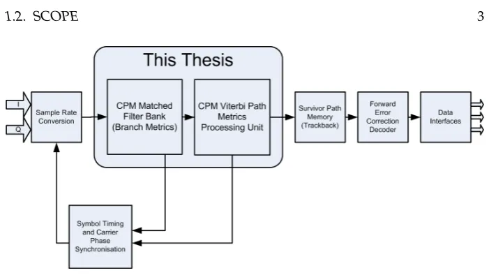
(19) 2. CHAPTER 1. INTRODUCTION. effective implementation is a challenge. The application has a stringent cost requirement that limits the implementation target to a Field Programmable Gate Array (FPGA) costing less than US$30 at a volume price. To demonstrate the proposed CPM configuration is able to meet the cost target, the two most computationally expensive receiver functions are implemented in VHDL and targeted to a Xilinx Spartan 3A-DSP 1800 FPGA. The designs are synthesised to confirm FPGA resource use and cost. Static timing analysis on the placed and routed netlist confirms data throughput. A VHDL functional simulation verifies operation of the implemented design. The literature tackles the complexity problem by using a variety of algorithm level complexity reduction techniques that have been shown to give significant reductions in complexity with a range of performance degradations relative to the maximum-likelihood receiver. Many of these techniques have not been tested in the presence of adjacent channel interference (ACI), and some complexity reduction techniques have shown increased sensitivity to ACI. This thesis avoids this issue and focuses on a maximum-likelihood FPGA implementation. This allows a dollar cost to be put on any quaternary CPM configuration with a symbol rate in the region of 10-30 MSymbols/s. This fills a gap in the literature where there are very few published details of CPM receiver FPGA implementations. A low-cost CPM filter bank FPGA implementation is proposed. It uses a distributed arithmetic technique to implement 27.6 giga-multiplies per second of filter bank multiplications consuming 23% of the available FPGA logic cells. A conventional approach would use the FPGA’s embedded multipliers but these resources provide a maximum of only 21 giga-multiplies/s. This design meets timing at 215.6 MHz, exceeding the minimum throughput requirements by 14%. The main drawback of this technique is that it adds one symbol period of processing latency. Since the branch metric filter bank is likely to be inside the phase recovery loop, this added latency degrades phase recovery performance. This is the price to be paid for a low-cost implementation. The Viterbi path metrics processing implementation follows a more standard architecture. The 128 state trellis is decomposed into 32 radix-4 units. Each radix-4 unit comprises 2 add-compare-select (ACS) units that calculate 4 path metrics every symbol period. This implementation uses 44% of the FPGA’s available logic cell resources. This design meets timing at 204.5 MHz achieving a throughput of 58.4 Mbit/s which is 8% more than the minimum requirement of 54 Mbit/s for the target application. Symbol and phase synchronisation for CPM is an ongoing area of research and is beyond the scope of this thesis; we assume ideal symbol and phase synchronisation.. 1.2. Scope. The purpose of this work is two-fold. Firstly, a new CPM configuration must be found that achieves a 50% spectral efficiency improvement over the existing product. Secondly, a practical, low-cost implementation must be demonstrated with an FPGA targeted VHDL implementation. In the search for an efficient CPM configuration we assume single-h CPM.
(20) 1.2. SCOPE. 3. Figure 1.1: CPM Receiver Functionality Studied in this Thesis and coherent reception. We assume perfect timing and carrier phase recovery and assume a zero carrier frequency offset. Although this is an active area of research it is beyond the scope of this thesis. The CPM configuration’s bandwidth consumption, SNR performance, Adjacent Channel and Co-Channel Interference (ACI, CCI) performance must meet an application specific set of ETSI standard requirements [1]. We assume 239/255 Reed Solomon forward error correction. The data rate requirement is 54 Mbit/s or 27 MSymbols/s for a quaternary CPM symbol alphabet. This provides for the transport of 24 E1 circuits and an additional approximately 5 Mbit/s for framing and auxiliary channel overhead. The VHDL implementation in this thesis focuses purely on the two most computationally expensive, and thus costly, functions of the CPM receiver. See Figure 1.1. This is the branch metrics filter bank and the Viterbi path metric add-compare-select functionality. Not included within the scope of this thesis are E1 data circuit interfaces, forward error correction, framing, sample rate conversion and front end band-limiting. Survivor path management is not implemented. A traceback architecture is cost effective because it uses FPGA block memory to store the Viterbi path history. Section 4.5 shows that the memory required to implement this function is small; one or two block rams for this application. Meeting throughput requirements is straight forward since this function is outside the Viterbi iteration loop and so the logic can be pipelined extensively. However, traceback memory bandwidth requirements are high when tracing back once every symbol. The bandwidth requirements can be reduced significantly by tracing back only once every several symbols using the technique described in [2]. The cost is added latency but this is negligible in the context of the latency through a complete receiver. Phase and timing recovery require early, tentative symbol decisions and these would not be generated by tracing back [3] [4]. The find-the-best metric operation has also not been implemented. If tracing back once every few symbols, bit-serial techniques are appropriate and the FPGA resources consumed can be kept to a minimum. Phase and timing recovery determine the constraints on this latency which is beyond the scope of.
(21) 4. CHAPTER 1. INTRODUCTION. Figure 1.2: Modelling and Implementation at Complex Baseband this thesis. For reasonable latencies, the cost of this operation is small relative to the rest of the receiver. The VHDL implementation is proved with synthesis results, static timing analysis and a VHDL functional simulation. This approach is justified in appendix A. All modelling and implementation is done at complex baseband as shown in Figure 1.2.. 1.3. Summary of Thesis Contributions. The main contribution of this thesis is a resource efficient and low-cost FPGA implementation of the two most computationally expensive components of a CPM receiver of moderate throughput (54 Mbit/s). The CPM configuration achieves a 50% increase in spectral efficiency over an existing product. Other contributions include: • Demonstration of a 50% spectral efficiency improved CPM configuration meeting a specific ETSI microwave radio standard which specifies requirements for tranmsitted power spectral density and receiver performance in the presence of channel noise and adjacent and co-channel interference. • CPM Viterbi demodulator fixed point simulation results. • The application of Hekstra’s path metric normalisation method to a CPM detector. • The application of a bit-serial distributed arithmetic filter algorithm to the FPGA implementation of a CPM branch metric unit. • Application of a Viterbi radix-4 decomposition to a CPM trellis.. 1.4. Overview. • Chapter 2 presents background material relevant to the work in this thesis. The CPM signal model is developed and the key equations for the.
(22) 1.4. OVERVIEW. 5. maximum likelihood receiver are stated. This chapter also contains a review of the CPM literature relevant to this thesis. • Chapter 3 investigates the choice of CPM parameters to improve spectral efficiency by 50%. Floating point models developed in Matlab and Simulink simulate the CPM transmitter and receiver at baseband. We choose the CPM configuration with lowest complexity that still meets the ETSI standard transmit power spectrum mask and receiver detection efficiency specification. • Chapter 4 begins the transition to a fixed point hardware implementation. Matlab simulation results demonstrate the effect on receiver detection efficiency of sampling rate, word-length and Viterbi path history depth. There is a direct tradeoff between hardware complexity and detection efficiency. This chapter concludes by selecting the most appropriate sample rate, word-length and path history depth to be used in the FPGA implementation to follow. • Chapter 5 presents the branch metrics filter bank VHDL implementation. A distributed arithmetic algorithm implements each filter in the filter bank. Synthesis results show that the FPGA resource use meets the cost requirement, and static timing analysis results confirm throughput. Functional simulation results demonstrate that the VHDL implementation matches the Matlab fixed point model precisely. • Chapter 6 describes the Viterbi path metric VHDL implementation. This trellis decode add-compare-select (ACS) processing is implemented using a state-parallel structure using radix-4 units comprising dual ACS units. Results from synthesis, static timing analysis and functional simulation demonstrate that this design meets requirements. • Chapter 7 concludes the work presented in this thesis and suggests possibilities of investigation for the future..
(23) 6. CHAPTER 1. INTRODUCTION.
(24) Chapter 2. Background and Related Work 2.1. Introduction. This chapter begins by introducing the CPM signal model used throughout this thesis. A maximum-likelihood receiver is presented that comprises a filter bank followed by a Viterbi trellis search. Practical implementations use the Viterbi algorithm with an implementation comprising a branch metric unit, Viterbi path metric processing unit and a survivor management unit. The second half of this chapter presents a review of the CPM literature relevant to this thesis.. 2.2. Notation. This thesis uses the notation in Table 2.1. <(x) =(x) x̃(t). real component of x. imaginary component of x. baseband complex envelope of passband signal x(t) where x(t) = <{x̃(t)ejωc t } and ωc is the carrier angular frequency. Table 2.1: Notation. 2.3. Continuous Phase Modulation Signal Model. A radio frequency (RF) carrier modulated by a baseband message carrying signal can be described by Equation (2.1). The amplitude a(t) and phase φ(t) of the carrier fc are available to be modulated by the message signal [5]. s(t) = a(t)cos(2πfc t + φ(t)). (2.1). An equivalent exponential notation is given in Equation (2.2) where s̃(t) is the baseband complex envelope and ωc is the RF carrier angular frequency. 7.
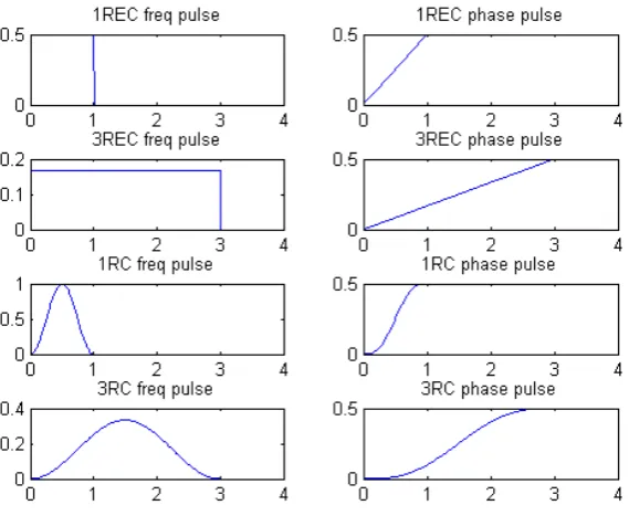
(25) 8. CHAPTER 2. BACKGROUND AND RELATED WORK. Equation (2.3) represents s̃(t) in terms of its in-phase and quadrature components and equivalently, Equation (2.4) shows the amplitude a(t) and phase φ(t) components explicitly. For the purposes of this thesis, all the interesting properties of the modulation are described by its complex envelope s̃(t) and so the passband formulation is not considered any further. s(t) = <{s̃(t)ejωc t }. (2.2). s̃(t) = sI (t) + jsQ (t). (2.3). s̃(t) = a(t)ejφ(t). (2.4). Keeping a(t) constant and using the message signal to modulate phase φ(t) only, the transmitted RF signal has a constant envelope and consequently is robust to non-linearities in the signal path. By smoothly transitioning the phase from symbol to symbol the spectral occupancy is reduced. This is continuous phase modulation [6]. The standard definition for how the phase is modulated by the message signal is defined in Equation (2.5). The message signal is represented as digital data coded into M-ary symbols a, coming from a symbol set of size M, as defined by equation (2.6). In this thesis M is considered a power of 2 only. φ(t, a) = 2πh. ∞ X. αi q(t − iT ). (2.5). i=−∞. αi ∈ {±1, ±3, ..., ±(M − 1)}. (2.6). The modulation index, h, is a parameter that trades off bandwidth and energy performance. Although it is possible to vary h from symbol to symbol, we only consider CPM schemes with a single, fixed h [7] 1 . q(t) is the all important phase smoothing function or phase pulse. Two examples are shown in Figure 2.1. For example, the raised cosine frequency pulse is described by Equation (2.7). The phase pulse is defined by Equation (2.8). This function starts at 0 at the beginning of a symbol duration so that the phase is continuous from one symbol period to the next. By convention this function is 1/2 at the end of the symbol duration. An infinite number of phase smoothing functions are possible but there are several standard pulses defined in the literature. g(t) =. 1 2πt (1 − cos( )), 0 ≤ t ≤ LT 2LT LT Z t q(t) = g(τ )dτ. (2.7) (2.8). −∞. The frequency pulse g(t) has finite duration of length LT where T is a nominal symbol period. The symbol period relates to the data bit rate and alphabet 1 If h is allowed to vary from one symbol to the next, it is called multi-h CPM. Further gains in spectral efficiency and energy consumption are possible, at the expense of further complication in the receiver[8]..
(26) 2.3. CONTINUOUS PHASE MODULATION SIGNAL MODEL. 9. Figure 2.1: Raised Cosine (RC) and Rectangular (REC) Frequency Pulse and Phase Pulse.
(27) 10. CHAPTER 2. BACKGROUND AND RELATED WORK. size as in Equation (2.9). L controls the degree of overlap between consecutive symbols in the modulator. CPM schemes with L = 1 are called full response and those with L > 1 are called partial response. CPM schemes with L > 1 spread the phase pulse in time and reduce the bandwidth of the transmitted signal [9]. The use of partial response CPM systems yields a more attractive tradeoff between error probability and spectrum than does the full response systems [9]. log2 M (2.9) bitrate A CPM configuration is uniquely defined by the three parameters h, M and q(t). These parameters must be chosen to meet the requirements of the application at hand. Chapter 3 investigates the choice of these parameters with regard to meeting spectral occupancy, SNR performance and cost requirements for a specific point to point microwave radio application. T =. 2.4. Maximum Likelihood Receiver. In this thesis we are interested in an implementation of the maximum-likelihood receiver. This is presented below. The received signal r̃(t) is a distorted version of the transmitted signal s̃ in the presence of additive white gaussian noise (AWGN) ñ(t), as shown by equation (2.10). We assume perfect channel equalisation, and we set the phase and time offset terms to zero, implying perfect timing recovery and perfect carrier phase synchronisation with no carrier frequency offset. Appendix C shows how the transmitted baseband signal, s̃, is generated in practice. r̃(t) = s̃(t, α) + ñ(t). (2.10). In [6], a maximum likelihood sequence estimating (MLSE) receiver is derived and it requires finding the symbol sequence α that maximises the correlation in Equation (2.11). This is a correlation of the received signal with all possible transmitted signals. Z ∞ J(α) = <{ r̃(t)s̃∗ (t, α)dt} (2.11) −∞. The number of symbol sequences grows exponentially with the sequence length making a receiver using a direct implementation of this equation impractical. By taking an iterative approach as in Equation (2.12), and performing the correlation over one symbol period at a time as in Equation (2.13), the receiver becomes practical. The index n identifies a single symbol period. Jn (α) = Jn−1 (α) + Zn (α) Z Zn (α) = <{. (2.12). (n+1)T. nT. r̃(t)s̃∗ (t, α)dt}. (2.13).
(28) 2.4. MAXIMUM LIKELIHOOD RECEIVER. 2.4.1. 11. Rational h. A further requirement is for h to be rational so that s̃∗ (t, α) lies within a finite set of waveforms over a single symbol period, making Equation (2.13) realisable. By restricting h to be rational according to Equation (2.14) then the phase takes on a finite set of phases modulo 2π at symbol time boundaries and a trellis with a finite number of states can be used to represent the phase transitions. h=. 2k , k, p ∈ integers p. (2.14). For CPM we have s̃(t) = ejφ(t). (2.15). where ∞ X. φ(t, a) = 2πh. αi q(t − iT ). (2.16). i=−∞. And when h is rational the phase signal can be divided into two terms as shown in Equation (2.17). φ(t, a) = 2πh. n X. αi q(t − iT ) + 2πh. n−L X. αi q(LT ). (2.17). i=−∞. i=n−L+1. θ(t, a) in Equation (2.18) describes how the phase changes during the nth symbol interval due to the current αn symbol and the previous L − 1 symbols. n X. θ(t, a) = 2πh. αi q(t − iT ). (2.18). i=n−L+1. θn in Equation (2.19) is the accumulated phase change due to all symbols prior to and including the an−L symbol. This is called the phase state. 2 n−L X. θn = πh. αi. (mod 2π). (2.19). i=−∞. φ(t, a) = θ(t, a) + θn. (2.20). Placing Equation (2.20) into Equation (2.13) gives Equation (2.21). Z Zn (αn , θn ) = <{. (n+1)T. r̃(t)e−j[θ(t,αn )+θn ] dt}. (2.21). nT. Zn (αn , θn ) = <{e. −jθn. Z. (n+1)T. r̃(t)e−jθ(t,αn ) dt}. (2.22). nT. Since αn can take on M L different sequences and θn takes on p different values, Equation (2.22) represents M L complex matched filters followed by p phase rotations [9]. 2 In general, θ does not represent the actual signal phase at the start of a symbol period ben cause θ(t, a) is non-zero at the beginning of a symbol period. The phase state is the cumulative contribution of past symbols to the signal phase up to L-1 symbols prior to the current time..
(29) 12. CHAPTER 2. BACKGROUND AND RELATED WORK. 2.4.2. Viterbi Trellis Decode. The Viterbi algorithm is an efficient way to evaluate Equation (2.12). Jn (α) represents the accumulated path metrics at time nT and Zn (α) is the set of branch metrics for the interval from t = nT to t = (n + 1)T . The trellis state is defined by Equation (2.23) where the phase state θn is defined by Equation (2.24) and the correlative state is defined by Equation (2.25). This gives a Viterbi trellis with pM L−1 states [9]. σn = (θn , αn−1 , αn−2 , . . . , αn−L+1 ) θn =. 2πi , i ∈ {0, 1, 2, . . . , p − 1} p. CorrelativeState = (αn−1 , αn−2 , . . . , αn−L+1 ). 2.5. (2.23) (2.24) (2.25). Viterbi Decoder Architecture. In the literature, Viterbi decoder implementations are typically treated by partitioning the functionality into three parts as shown in Figure 2.2. • Branch Metric Unit (BMU) - Computes hamming or Euclidean distance between the received symbol and the various possible transmitted symbols. For a CPM receiver this implements Equation (2.21). • Path Metric Processing Unit - Accumulates the path metric and selects a survivor path from each of the trellis connections inbound to each state. The path metrics are accumulated as defined by Equation (2.12). • SMU or TBU - Survivor management unit or Traceback unit. These units extract the decoded data from the ultimate survivor path.. Figure 2.2: Standard Viterbi Decoder Implementation Architecture.
(30) 2.6. LITERATURE REVIEW. 2.6 2.6.1. 13. Literature Review CPM Receiver Implementations. Nova Engineering use a multi-h CPM waveform to increase spectral efficiency by 3 times compared to legacy PCM/FM telemetry waveforms at the same detection efficiency. They use a modulation index of h=1/4,5/16, a raised cosine phase pulse of 3 symbol periods (L=3RC) and a quaternary alphabet (M=4). Viterbi trellis complexity is 512 states [10]. Nova Engineering have also designed a product called Hypermod MMD22 which uses multi-h CPM with M=4 and 128 state Viterbi trellis complexity. The complete transceiver is implemented on a board with 5 Xilinx Virtex E XCV2000E 3 FPGAs. One FPGA is allocated to the Viterbi trellis update calculations which consume 80% of the logic resources and 40% of the block ram. The data rate is 22 Mbit/s [11]. In [12], turbo-detected coded CPM is used in a military UHF satellite communications application. A data rate of 80 kbit/s is transmitted in a 25 kHz Eb of 11 dB, the bit error rate is 10−5 . They use M=8, h=1/8 and channel. At N o a rectangular phase pulse of 1 symbol duration (L=1REC). The modem implementation consists of 2 VERSA-module Europe (VME) cards in a VME chassis. Most of the signal processing functions are performed by a TMS320C6701 DSP but the iterative decoder is implemented in VHDL and uses 70% of an XCV2000E FPGAs resources. Because these are commercial products, very few details of these FPGA implemenations have been published. 2.6.1.1. Viterbi Path Metric Processing. There is a large body of literature describing algorithms and implementation details for Viterbi trellis decoding, mostly targeting the decoding of convolutional codes and for ASIC implementation. Although few papers were found that directly address the implementation of a CPM Viterbi trellis, many of the general Viterbi results are applicable. For low data rates or small Viterbi trellises, a fully state-serial approach uses the least hardware resources. A 64 state Viterbi decoder was implemented using a single add-compare-select (ACS) processing unit targeting a Xilinx Spartan 3 FPGA. The implementation used only 128 slices (approximately 256 logic cells) and 2 block rams to support a data rate of 2.4 Mbit/s [13]. In contrast, the CPM application in this thesis calls for a Viterbi decoder with a large number of states (128) and for a throughput of 54 Mbit/s which is moderately high for a low-cost FPGA implementation target. The traditional approach to high throughput, large trellis size Viterbi decoders is a fully state-parallel approach in which each state is processed with individual addcompare-select units. This consumes a lot of hardware resources and the ACS 3 An. XCV2000E has 38400 logic cells and supports a 130 MHz clock rate with 4 LUT levels. Although this FPGA is almost 10 years old, this part is roughly equivalent in density and performance to a Spartan 3-ADSP XC3S1800ADSP, the FPGA implementation target in this thesis. Virtex FPGA’s are Xilinx’s premium brand so offer higher performance than the spartan family, but at significantly higher cost..
(31) 14. CHAPTER 2. BACKGROUND AND RELATED WORK. path metric routing is complicated. A bit-serial approach to the ACS processing reduces the hardware requirements enormously, whilst also reducing the amount of ACS to ACS connectivity required since only a 1 bit wide path metric bus is required [2] [14]. However, this bit-serial approach does put an upper limit on throughput, dependent on the path metric wordlength. By using multiple ACS units where each ACS unit processes multiple states, a hybrid of the fully state-serial and state-parallel approaches is possible. Shung proposes a systematic approach to allocating states to ACS units. By pipelining the ACS operation a single ACS unit processes multiple states at once. It is claimed this provides a favourable area-time tradeoff [15]. In general, a Viterbi trellis can be decomposed into radix-k sub-units, where k is a power of 2. For example, a radix-2 trellis has 2 inbound and 2 outbound paths per state and the radix-4 form of this trellis has 4 inbound and 4 outbound paths per state. Each Viterbi iteration of a radix-4 trellis is equivalent to 2 iterations of the radix-2 trellis. In this way a radix-4 trellis doubles the available time to perform the ACS operations. [16] is an ASIC implementation that nearly doubles throughput by decomposing a 32 state convolutional code radix-2 trellis into a radix-4 trellis. They achieve a decoding throughput of 140 Mbit/s in 1.2um CMOS. All ACS units within a radix-4 unit share input path metrics keeping all routing within a radix-4 unit local. This thesis shows that the natural radix-4 decomposition of the CPM trellis used in our microwave radio application, brings the same advantages to a CPM trellis Viterbi decoder. Survivor path traceback has been regarded as another bottleneck to throughput. However, by increasing the survivor path memory size and tracing back less often than once per symbol, the traceback memory bandwidth requirements may be reduced significantly [2]. Sub-optimum detection based on the T-algorithm has been applied to the VLSI implementation of a coherent CPM detector [17]. Another non maximumlikelihood technique is the adaptive Viterbi algorithm which reduces the average amount of computation required by searching a subset of the full trellis based on channel conditions [18] [19] [20]. A systolic array approach to the branch metric and path metric processing is proposed in [21]. Both of the two main SRAM based FPGA vendors, Altera and Xilinx, have developed Viterbi Decoder IP cores. The Altera core can implement a 256 state trellis with a throughput of 16 Mbit/s using 3800 logic cells and 18 9-kbit block rams in a Cylone III family FPGA (EP3C10F256C6). They use 3 bit branch metrics [22]. Xilinx’s serial IP core implements a 64 state trellis using 983 slices (equivalent to approximately 1966 logic cells) at a throughput of 15 Mbit/s in a Spartan 3A-DSP family FPGA (XC3SD3400A-4) [23]. 2.6.1.2. Viterbi Path Metric Normalisation. The Viterbi path metrics grow without bound over time. Several techniques have been developed for scaling or normalising the metrics so they can be represented in fixed point arithmetic [24]. Since only the difference between path metrics is required for path selection in the Viterbi add-compare-select unit, and because this difference is bounded, Hekstra proposes the use of 2’s complement arithmetic as an alternative to scaling or normalisation. This method eliminates the need for additional normalisation or rescaling hardware [25]. Path metric difference bounds are required to size the path metric wordlength.
(32) 2.6. LITERATURE REVIEW. 15. [26]. It has not been shown that these techniques can be applied to a CPM Viterbi trellis.. 2.6.2. CPM Configurations and their Energy/Bandwidth Consumption. Aulin and Sundberg [27] [9] show a method for calculating a CPM code’s minimum distance which predicts detection efficiency. They also plot various CPM codes on the energy bandwidth plane. Anderson, Aulin and Sundberg [6] [7] show results for a wider variety of CPM configurations on the energy bandwidth plane, mostly using the raised cosine (RC) phase pulse. However, they do not measure performance against ETSI microwave radio standards. Svensson [28] considers the choice of CPM configuration with regard to meeting a spectral mask requirement, seemingly also from the same ETSI specification [1] as required in our application. They target 37.5 Mbit/s in a 14 MHz channel (2.68 bits/s/Hz) whereas the application in this thesis requires 54 Mbit/s in a 28 MHz channel (1.93 bits/s/Hz). They also provide results for adjacent channel interference with a carrier to interference ratio the same (-5dB) as required for the application considered in this thesis. Strangely, they locate the interferer at the 2nd adjacent channel whereas the ETSI specification calls for a 1st adjacent channel interferer. Svensson [29] develops an empirical model for CPM and shows that for a constant effective bandwidth, M=8 is the optimum power of 2 symbol alphabet size in the range from 4 to 32, in order to maximise minimum distance squared (detection efficiency). However, compared to M=4, the advantage in terms of d2 min of M=8 is only 0.55 dB. They also describe a saturation L, beyond which brings little improvement to d2 min. For M=8 it is 3, and for M=4 it is 7. However, for M=4 the advantage of L=7 over L=4 is only .57 dB. Optimising the shape of the phase pulse has been investigated. In [30] an optimised phase pulse for M=8, L=3 and h=1/8 gave only a 0.2dB gain over a GMSK phase pulse. For other M, gains up to 0.9 dB were found. [31] also investigates optimised phase pulses but concluded “the commonly known signal shapes are not too far from optimal performance”. Multi-h CPM is summarised in [8] and shows for the same bandwidth consumption, multi-h CPM has about a 2 dB d2 min improvement for M=4, 3RC, across a range of h. However, the increase in receiver complexity is considered beyond the scope of this thesis.. 2.6.3. Complexity Reduction. Spectrally efficient CPM configurations have a non-binary symbol alphabet and smooth phase pulses lasting multiple symbol periods which leads to maximumlikelihood receivers with high complexity [7]. There is a significant body of literature proposing reduced complexity detectors, summarised by Perrins in [32]. The size of the receiver matched filter bank has been reduced by truncating the phase pulse and also by using a modified and reduced set of basis functions [33] [34]. The number of Viterbi trellis states has been reduced by.
(33) 16. CHAPTER 2. BACKGROUND AND RELATED WORK. searching only a subset of the full trellis or by using decision feedback [35] [36] [6]. Combining these techniques have been studied in [32] [37] [28]. Laurent proposed a pulse amplitude representation [38] and by ignoring the smaller amplitude pulse receiver complexity is reduced. This was extended to M-ary CPM by Mengali [39]. Kaleh [40] presents a near optimum reduced complexity Viterbi receiver based on the PAM decomposition. Other than in [28], adjacent channel interference performance of these reduced complexity schemes has not been tested. For a carrier to interference ratio of -5 dB, their 64 state detector has approximately only 0.5 dB loss; the maximum-likelihood detector is 1280 states. Unfortunately, they place the interferer in the 2nd adjacent channel but in our application there is the far more stringent requirement of the interferer being in the 1st adjacent channel. Also, Simmons claims the reduced trellis size decoders have significantly increased susceptibility to adjacent channel interference (ACI) [41], although the carrier to interference levels used were large (-10 and -20 dB).. 2.6.4. Literature Review Summary. Bandwidth and energy consumption of CPM configurations are well studied, and a few papers evaluate the CPM codes bandwidth properties against ETSI standard spectral masks. As one would expect, CPM code performance has not been evaluated against the specific 28 MHz ETSI channel that is the focus of the microwave radio application considered by this thesis. Although there is a vast range of Viterbi decoder literature, there are few published details for FPGA targeted CPM receiver implementations. There were no published results found for fixed point CPM receiver models. Several techniques for complexity reduction give large reductions in complexity with minimal performance degradation, however adjacent channel interference performance of these algorithms is largely unproven. This thesis avoids this issue by implementing a maximum-likelihood receiver and focusing on a low-cost, resource efficient FPGA implementation. The CPM literature typically measures complexity in terms of the number of matched filters and Viterbi states. This is a limitation for the purpose of this thesis since here we must meet a specific cost requirement. FPGA cost and resource use is measured in logic cells and block rams rather than the number of Viterbi states or branch metric filters..
(34) Chapter 3. Improving Spectral Efficiency: CPM Parameter Selection 3.1. Introduction. In microwave radio cellular backhaul applications, improving spectral efficiency is desirable, as long as receiver detection efficiency and interference sensitivity are not compromised. An increase in spectral efficiency means the same data rate can be transported using less bandwidth allowing the operator to lower costs by using less costly radio spectrum licenses. Alternatively, operators keep constant their use of the already limited radio spectrum, and provide higher data rates to support, for example, the growing demand for mobile data services. An existing CPM microwave radio product transports 16 E1 data circuits (36 Mbit/s including overhead) in a ETSI 28 MHz channel. This is a nominal spectral efficiency of 1.3 bits/s/Hz. This modem achieves a 10−6 bit error rate (BER) at an SNR of 14 dB [42]. In this chapter, we show a 50% higher data rate, 24 E1 data circuits (54 Mbit/s including overhead), can be transported in the same 28 MHz channel without any degradation in receiver detetection efficiency. This provides a margin of 4.7 dB to the ETSI receive signal level threshold specification assuming a radio noise figure of 6 dB. The spectral efficiency is improved to 1.9 bits/s/Hz by moving to a new CPM configuration with a longer duration phase pulse and a smaller modulation index. Both these factors reduce detection efficiency; this degradation is mitigated by moving to coherent CPM demodulation. We assume perfect timing and carrier phase recovery and assume a zero carrier frequency offset. Others have attempted more ambitious schemes such as 37.5 Mbit/s in a 14 MHz channel; this is a spectral efficiency of 2.7 bits/s/Hz. However, the optimum detector for this scheme is complicated requiring 2048 matched filters and a Viterbi decoder of 1280 states. A reduced complexity approach was taken resulting in a detector that is not maximum-likelihood. Also, only 2nd adjacent channel interference (ACI) sensitivity was investigated; the microwave radio application in this thesis requires compliance with a more stringent 1st adjacent channel interference sensitivity specification [28]. 17.
(35) 18. CHAPTER 3. CPM PARAMETER SELECTION. There are a large number of CPM configurations that potentially meet our requirements. Symbol alphabets of 2, 4 or 8 have been used in real world implementations, phase pulse durations from 1 to 5 symbol periods, phase pulse shapes of raised cosine, rectangular, GMSK and others, and a wide range of modulation indexes are possible [10] [11] [12] [28] [32]. This chapter chooses a CPM configuration that meets the ETSI channel transmit spectral mask and interference rejection requirements, whilst providing an acceptable tradeoff between detection efficiency and receiver implementation complexity measured in terms of the Viterbi trellis and branch metric matched filter bank size. This chapter starts by identifying 4 candidate CPM configurations by examining their theoretical detection and bandwidth efficiency. These candidate configurations are then simulated and their performance evaluated against an ETSI standard specifying limits for transmit power spectrum, interference sensitivity and receive signal threshold performance. The CPM configuration of h=1/4, L=3RC, M=4 is chosen because it meets the ETSI requirements, and has the lowest complexity of any scheme that exceeds the ETSI receive signal threshold requirements by more than 4 dB.. 3.2. Analytical CPM Performance: Identifying CPM Configuration Candidates. There is a large number of possible CPM configurations, each with its own specific detection efficiency and bandwidth consumption characteristics. There are 4 parameters that specify a CPM configuration: • Symbol Alphabet Size (M) • Modulation Index (h) • Phase Pulse Duration (L) • Phase Pulse Shape These 4 parameters are reflected in the standard equation for how the phase of a CPM modulated signal changes with time and data symbols; see Equation (3.1). q(t) determines the shape of the phase pulse and αi is a data symbol from an alphabet of size M. “n” refers to the nth data symbol transmitted. θ(t, a) = 2πh. n X. αi q(t − iT ). (3.1). i=n−L+1. Continuous phase modulation is a coded modulation and by calculating a CPM configuration’s minimum Euclidean distance, relative detection efficiency performance comparisons can be made. Symbol error rate is derived from the minimum distance squared, d2 min, as shown in Equation (3.2). The procedure for calculating a CPM configuration’s minimum distance is well documented[6]. For the purposes of this thesis, this was implemented in Matlab ; Appendix E.1.1 contains the source code. r Eb (3.2) Pe ≈ Q( d2 min ) N0.
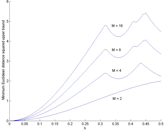
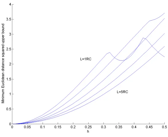
(36) 3.2. CPM CANDIDATES. 19. Figure 3.1: Effect of Symbol Alphabet Size (M) on Detection Efficiency, L=1, Raised Cosine Phase Pulse Figure 3.1 illustrates how M and h affect detection efficiency for L=1 and a raised cosine (RC) phase pulse. Increasing M improves detection efficiency and the general trend for increasing h is an increase in detection efficiency. Increasing these parameters also causes an increase in bandwidth consumption. It is worth noting that this is an upper bound. At certain so-called “weak” modulation indices d2 min no longer reflects actual symbol error rate performance. None of the CPM configurations considered in this thesis fall into this category [6]. Figure 3.2 shows the effect of phase pulse durations from 1 to 5 nominal symbol periods for a quaternary alphabet and raised cosine phase pulse. The effect of a longer, smother phase pulse is to reduce detection efficiency; the flip side is a reduction in bandwidth consumption [6]. It is clear that in order to choose a CPM configuration it is necessary to evaluate it in a combined detection and bandwidth efficiency sense.. 3.2.1. Choice of Symbol Alphabet Size (M) and Phase Pulse Shape. In this thesis, only a quaternary symbol alphabet (M=4) is investigated. This is almost certainly superior to a binary symbol alphabet (M=2). Across a range of modulation indices, M=4, L=3RC has almost 3dB better detection performance compared to M=2, L=3RC when comparing CPM configurations with the same.
(37) 20. CHAPTER 3. CPM PARAMETER SELECTION. Figure 3.2: Effect of Phase Pulse Duration (L) on Detection Efficiency, M=4 bandwidth consumption [6]. An empirical model was developed that shows M=8 may be the best even-integer alphabet size [29]. However, in the example given it is only 0.55 db better than M=4 yet has substantially higher complexity so is not considered further. 1 There are an infinite number of possible phase pulses although there are a standard few described in the literature: raised cosine (RC), spectrally raised cosine (SRC), rectangular (REC), Gaussian minimum shift keying (GMSK), tamed frequency modulation (TFM) and continuous phase frequency shift keying (CPFSK). Raised cosine is arguably the most popular and is often used as the baseline for comparison [6]. A phase pulse shape optimised to the bandwidth and detection efficiency requirements is possible but Asano concludes “the commonly known signal shapes are not too far from optimal performance” [31]. In any event, the implementation proposed in Chapters 5 and 6 supports alternative phase pulses. The phase pulse shape is reflected in the matched filter bank coefficients which are stored in volatile memory. The design can be easily modified to support external reloading of this memory. For these reasons, the choice of phase pulse is not investigated; the simulations and FPGA 1 M=8 has higher complexity since the number of matched filters and Viterbi states increases exponentially with M. However, an advantage of moving to M=8 is that the symbol rate drops by 50% since the number of bits per symbol increases by 50%. This eases the throughput requirement on the implementation since the amount of processing time available for each symbol is now %50 higher. This is particularly significant for the Viterbi iteration loop since it contains feedback that causes a bottleneck in pipelined FPGA implementations..
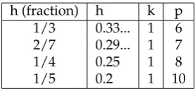
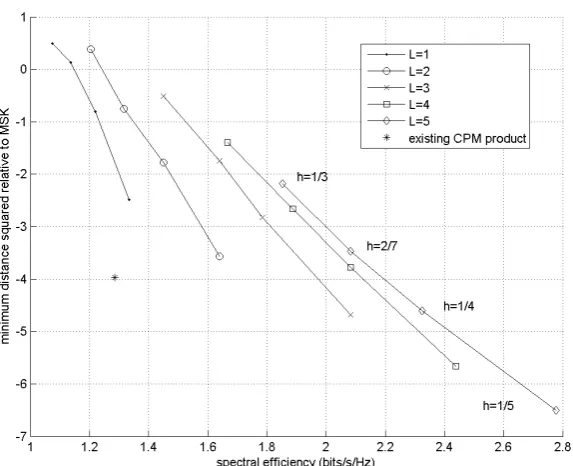
(38) 3.2. CPM CANDIDATES h (fraction) 1/3 2/7 1/4 1/5. 21 h 0.33... 0.29... 0.25 0.2. k 1 1 1 1. p 6 7 8 10. Table 3.1: Candidate Modulation Indices (h) implementations in this thesis use a raised cosine phase pulse. 2 We have chosen a quaternary alphabet (M=4) and a raised cosine phase pulse. Candidates for the modulation index (h) and phase pulse duration (L) are selected next.. 3.2.2. Modulation Index (h) and Phase Pulse Duration (L) Candidates. In order to identify modulation index and phase pulse duration candidates, the CPM configuration must be evaluated in a combined detection efficiency and bandwidth efficiency sense. Bandwidth of the transmitted baseband CPM signal is calculated using a numerical method described in [7, pg 231]. We define the double-sided bandwidth as the bandwidth containing 99% of the transmitted power. This numerical method was implemented by the author using Matlab; Appendix E.1.2 contains the source code listing. For coherent reception, the modulation index must be of the form h = 2k p where k and p are integers. The modulation indices considered are shown in Table 3.1. Modulation indices above this range consume too much bandwidth and values below this range have too low a detection efficiency. There are other k, p combinations that sit within this range, but all require large values of p and so are considered too costly in terms of implementation. For example, 3 h = 11 = 0.27 is interesting, but when put into the form h = 2k p , k=3 and p=22. 22 phase states is considered too costly for implementation. Phase pulse durations from the range 1 to 5 symbols are considered. Combined with the 4 modulation index values of Table 3.1 gives 20 CPM configurations to be evaluated. All configurations are evaluated in a combined detection efficiency and spectral efficiency sense with the results shown in Figure 3.3. Detection efficiency is calculated in terms of d2 min relative to minimum shift keying (MSK). MSK has a d2 min of 2. Spectral efficiency is calculated from the bandwidth calculation described above. The existing CPM product’s performance is also plotted in Figure 3.3. The spectral efficiency of the CPM product is calculated as the symbol rate data rate (36 Mbit/s) divided by the ETSI channel bandwidth (28 MHz). When comparing the existing CPM product’s spectral efficiency with these new CPM configurations, there is an assumption that the transmit power spectrum determines the channel spacing. This is not necessarily true as adjacent channel 2 The current FPGA design uses a LUT4 primitive to store the matched filter coefficients. By replacing the LUT4 with an SRL16 primitive the filter coefficients can be loaded serially, yet still read and addressed as a standard memory..
(39) 22. CHAPTER 3. CPM PARAMETER SELECTION. Figure 3.3: Relative Detection Efficiency and Spectral Efficiency for several CPM Configurations. interference tolerance may require the transmitted bandwidth to lie some extra distance inside the transmit channel mask. The existing CPM product’s detection efficiency relative to MSK is approximated by calculating its equivalent d2 min using the existing products threshold performance of 14 dB SNR at 10−6 bit error rate and Equation (3.2) solved for d2 min. This is an approximation because the threshold performance is specified at a bit error rate, whereas Equation (3.2) calculates a symbol error rate. The first point to note is that h acts to tradeoff detection efficiency and spectral efficiency. Only by increasing L can both detection efficiency and spectral efficiency be improved. However, the gains get less and less at each higher L, while the complexity increases exponentially with L [6]. CPM configurations with L=4 or L=5 are ruled out as their complexity is considered too high. Indeed, Chapters 5 and 6 implement a CPM configuration with L=3 that meet the cost requirement for the application in this thesis. Moving to L=4 increases the complexity by 4 times which would cause the cost requirement to be exceeded. There are only 4 remaining CPM configurations that are in the vicinity of meeting the 50% increase in spectral efficiency goal of 1.9 bits/s/Hz. These are listed in Table 3.2. Three of the 4 schemes promise to improve detection efficiency compared with the existing CPM product. This table also shows the maximum-likelihood receiver complexity in terms of matched filters and Viterbi trellis states..
(40) 3.3. ETSI REQUIREMENTS h 1/5 2/7 1/4 1/5. L 2 3 3 3. M 4 4 4 4. no. matched filters 32 128 128 128. 23 no. Viterbi trellis states 40 112 128 160. Table 3.2: Candidate CPM Configurations. 3.3. CPM Configuration Evaluation Metrics: ETSI Compliance. A floating point Simulink model is used to carry out simulations confirming the analytical detection efficiency and bandwidth consumption results presented in the previous section and evaluate the candidate CPM configurations against an ETSI microwave radio standard. The cellular backhaul microwave radio application considered in this thesis requires a product to meet this standard. The ETSI specification [1, Annex D] constrains three aspects of the modulation: 1. Bandwidth - The transmitted power spectrum must fit within a low-pass spectral mask. 2. Detection Efficiency - At a specified received signal power level, the receiver bit error rate (BER) must be less than a specified value. 3. Interference Rejection - In the presence of adjacent channel interference (ACI) or co-channel interference (CCI), detection efficiency can degrade by no more than specified limits. It is worth noting that the ETSI detection efficiency specification is the minimum performance required to achieve ETSI compliance. System gain is an important product marketing specification, and since improvements to detection efficiency (receiver sensitivity) directly improve system gain, it is desirable to maximise the margin to this specification. For example, improving the detection efficiency by 3 dB allows the use of an antenna approximately half the size and therefore significantly reduced cost. The chosen CPM configuration must meet the ETSI requirements whilst providing an acceptable tradeoff between detection efficiency and receiver implementation complexity and cost.. 3.3.1. Specific Application. The specific application of interest to this thesis is covered by the ETSI standard: Fixed radio systems, Characteristics and requirements for point-to-point equipment and antennas. The frequency bands of interest are 13 GHz and 15 GHz which are covered by Annex D of this standard. Our 50% improved spectral efficiency CPM configuration transports 24 E1 circuits within the 28 MHz channel. The ETSI standard classifies such a system as spectrum efficiency class 2, system D.1. MHz channel [1, Annex D]..
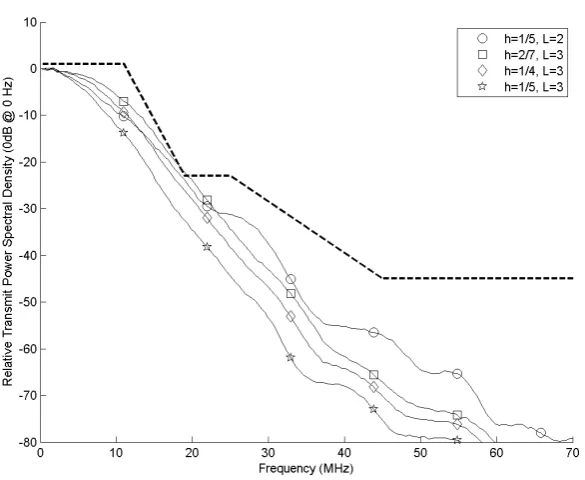
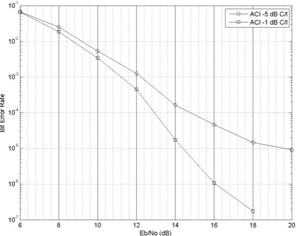
(41) 24. CHAPTER 3. CPM PARAMETER SELECTION interference type. co-channel co-channel 1st adjacent channel 1st adjacent channel. carrier to interference ratio (dB) 23 19 0 -4. allowed SNR degradation (dB) 1 3 1 3. new SNR (dB) 19.7 21.7 19.7 21.7. new Eb No (dB) (M=4) 16.7 18.7 16.7 18.7. Table 3.3: ETSI Co-Channel and 1st Adjacent Channel Interference Performance [1, Table D.7]. 3.3.2. Bandwidth: Transmit Power Spectral Density (PSD). The transmitted signal must lie within the radio frequency spectrum mask shown in Figure 3.5. The channel spacing is 28 MHz. This mask is specified relative to the carrier frequency fo . The transmitted spectrum is assumed to be symmetrical and so only single sided limits are specified. The 0dB point on the mask corresponds to the power spectral density (PSD) at the carrier frequency [1, Table D.4]. In this thesis the transmitter is modelled at baseband and so the simulated baseband transmit power spectrum is directly evaluated against the spectrum mask shown in Figure 3.5. It is assumed the up-conversion process does not alter the shape of the transmitted power spectrum.. 3.3.3. Detection Efficiency: Bit Error Rate as a function of Receive Signal Level. It is widely known that in general, detection efficiency performance can be traded off against bandwidth efficiency performance. Section 3.3.2 constrains the bandwidth and here we constrain detection efficiency; at a receive signal level of -75 dBm, the bit error rate (BER) must be less than 10−6 [1, Table D.6]. For the purposes of simulation, -75 dBm receive signal level is equivalent Eb to a signal to noise ratio (SNR) of 18.7 dB and energy per bit to noise ratio ( N ) o of 15.7 dB. Appendix B details this calculation.. 3.3.4. Interference Rejection. The radio must achieve a minimum level of detection efficiency in the presence of co-channel and adjacent channel interference. Table 3.3 specifies the strength of the interferer and the amount by which SNR may be degraded while still achieving a 10−6 bit error rate. In practice, the candidate CPM configurations are evaluated against a more stringent specification to provide engineering margin. We increase the carrier to interference ratios in Table 3.3 by 1 dB and bit error rate is measured without forward error correction (FEC) and is relaxed to 10−5 . This leaves approximately two orders of magnitude of BER margin before exceeding the error correcting capabilities of the Reed Solomon FEC. The code used has a threshold at about 10−3 ; a BER of 10−3 at the FEC input results in approximately 10−6 at the output..
(42) 3.4. SIMULATION RESULTS. 3.4. 25. Simulated CPM Performance: Selecting a CPM Configuration For Implementation. The simulation system model is presented first, followed by simulation results evaluating the candidate CPM configurations against the ETSI requirements. The h=2/7, L=3 configuration does not meet the spectral mask and so is rejected. The h=1/4, L=3 configuration meets all ETSI requirements and so meets the 50% increase in spectral efficiency target; the h=1/5, L=3 configuration has a smaller minimum distance so is rejected. The h=1/5, L=2 configuration does not meet the adjacent channel interference rejection requirement.. 3.4.1. Simulation System Model. The simulation system model is shown in Figure 3.4. The 6 key parts of this model are: • Transmitter - The transmitter comprises a linear feedback shift register data source of polynomial x15 + x14 + 1 , a Reed Solomon forward error correction encoder of codeword length (n) 255 and message length (k) 239, and a CPM modulator. The symbol rate is 27 MSymbols/s and 8 samples per symbol. • Receiver - The receiver comprises a low pass filter, CPM demodulator with traceback depth of 32 symbols and a Reed Solomon decoder. The low pass filter provides close-in adjacent channel rejection. • Channel - The channel is modelled with additive white Gaussian noise only. There is no channel delay. Phase and symbol synchronisation are ideal. • Interference Generator - A second transmitter model generates co-channel and adjacent channel interference. Gain, phase and frequency are adjustable. • Bit Error Rate (BER) Checker - Transmitted bits and symbols are compared with the received symbols and bits, both before and after FEC decoding to determine the symbol and bit error rate. • Transmit Power Spectral Density Measurement - Transmitter power spectral density is measured using a periodogram. The FFT length is 2048 samples, it uses a Hanning window and the periodogram averages over 256 spectra.. 3.4.2. Bandwidth: Transmit Power Spectral Density (PSD). The simulated baseband transmit power spectrum of the 4 candidate CPM configurations is shown in 3.5 together with the relevant ETSI spectral mask. Figure 3.6 is a zoomed in view of the same data and shows that h=2/7, L=3 CPM configuration is the only one that fails to meet the spectral mask..
(43) 26. CHAPTER 3. CPM PARAMETER SELECTION. Figure 3.4: Simulation System Model. Figure 3.5: Simulated Transmit Power Spectral Density of Candidate CPM Configurations, Various (h, L), M=4, 27 Msymbols/s).
(44) 3.4. SIMULATION RESULTS. 27. Figure 3.6: Zoomed in version of Figure 3.5. 3.4.3. Detection Efficiency and Interference Rejection Performance: h=1/4, L=3. 3.4.3.1. Detection Efficiency: Bit Error Rate as a function of SNR. With an AWGN channel only, simulated error rate performance is shown in Figure 3.7. The symbol and bit error rate data was collected by accumulating a minimum of 100 symbol errors, or for the FEC BER graph a minimum of 100 bit errors after FEC. The receiver low-pass filter is removed for this simulation. Eb A BER of 10−6 is achieved with an N of 14 dB. Furthermore, when the o Eb Reed Solomon FEC is included then No is approximately 10.6 dB at a BER of 10−6 . This is 5.1 dB better than the ETSI requirement of 15.7 dB.. The existing CPM modem product achieves a 10−6 BER at an SNR of 14 Eb dB or 11 dB N [42] assuming ideal timing synchronisation and no degradao tion due to fixed precision arithmetic. 3 These results show that the new CPM configuration has the potential to be 0.4 dB better in terms of detection efficiency. However, a low-pass adjacent channel rejection filter is required to meet the ACI rejection requirements. This filter also degrades clear channel performance as described in the next section. 3 SNR. is 3 dB higher than. Eb No. for a quaternary alphabet..
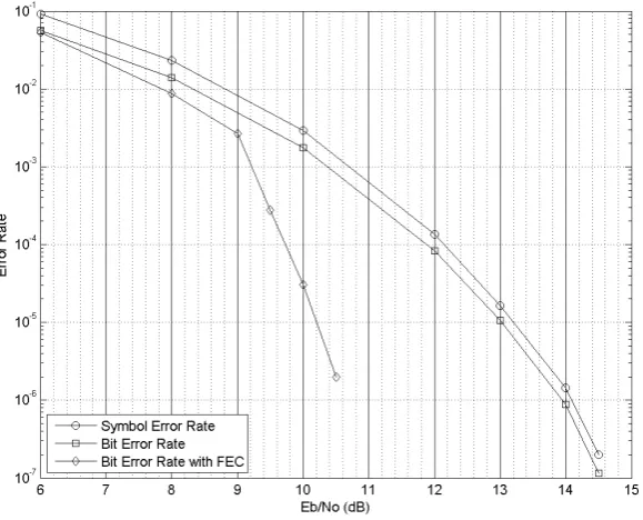
(45) 28. CHAPTER 3. CPM PARAMETER SELECTION. Figure 3.7: Simulated Bit Error Probability with and without Reed Solomon FEC, AWGN Channel, No ACI Reject Filter, h=1/4, L=3RC, 27 Msymbols/s.
Figure
+7

Related documents
The objective is to investigate whether enriched enteral nutrition given shortly before, during and early after colo- rectal surgery, reduces POI and AL via stimulation of the
proyecto avalaría tanto la existencia de una demanda real e insatisfe- cha de este servicio por parte de la población titular de derechos como la capacidad de ambos
This study proposed a systematic grounded theory approach to discover if students became motivated for reading by being given an opportunity to select reading content for
The work is not aimed at measuring how effective your local polytechnic is, but rather to see what measures different community groups, including potential students, use when
In this paper we find sea- sonal variability in two independent ice velocity data sets and we consider the potential roles of surface meltwater, ice shelf basal melt, and sea
The nutritive value in vitro organic matter digestibility, neutral detergent fibre and nitrogen content of Aries HD was similar to that of Yatsyn 1 perennial ryegrass, from
2 Equity Market Contagion during the Global Financial Crisis: Evidence from the World’s Eight Largest Economies 10..
4b (again, vehicle icons are not drawn to scale). This area was approximately 2. We analyzed scenarios with different vehicle densities per square kilometer, as specified in Table
