Abstract— Three-phase active rectifiers guarantee sinusoidal input currents and unity power factor at the price of a high switching frequency ripple. To adopt an LCL-filter, instead of an L-filter, allows using reduced values for the inductances and so preserving dynamics. However, stability problems can arise in the current control loop if the present resonance is not properly damped. Passive damping simply adds resistors in series with the LCL-filter capacitors. This simplicity is at the expense of increased losses and encumbrances. Active damping modifies the control algorithm to attain stability without using dissipative elements but, sometimes, needing additional sensors. This solution has been addressed in many publications. The lead-lag network method is one of the first reported procedures and continues being in use. However, neither there is a direct tuning procedure (without trial and error) nor its rationale has been explained. Thus, in this paper a straightforward procedure is developed to tune the lead-lag network with the help of software tools. The rationale of this procedure, based on the capacitor current feedback, is elucidated. Stability is studied by means of the root locus analysis in z-plane. Selecting the lead-lag network for the maximum damping in the closed-loop poles uses a simple optimization algorithm. The robustness against the grid inductance variation is also analyzed. Simulations and experiments confirm the validity of the proposed design flow.
Index Terms— voltage-source converter, rectifier, Active damping, LCL-filter, stability, lead-lag.
I. INTRODUCTION
HREE phase voltage source converters guarantee sinusoidal currents and unity power factor resulting suitable for distributed power generation [1],[2] and smart grid environments [3]. However, this is at the price of a high frequency switching
R. Peña-Alzola is with Department of Energy Technology, Aalborg University, DK-9220 Aalborg East, Denmark (e-mail: [email protected]).
M. Liserre is with Department of Energy Technology, Aalborg University, DK-9220 Aalborg East, Denmark (e-mail: [email protected])
F. Blaabjerg is with the Department of Energy Technology, Aalborg University, DK-9220 Aalborg East, Denmark (e-mail: [email protected]).
R. Sebastián is with the Department of Electrical, Electronic and Control Engineering, National University for Distance Learning, UNED, 28040-Madrid, Spain (e-mail: [email protected]).
J. Dannehl is with Danfoss Solar Inverters A/S, DK-6400 Sønderborg, Denmark (e-mail: [email protected]).
F. W. Fuchs is with the Institute for Power Electronics Electronics. and Electrical Drives, Christian-Albrechts-University of Kiel, 24143 Kiel, Germany (e-mail: [email protected]).
ripple [4]. The use of L-filters to limit the harmonic current injection to the grid calls for large and heavy inductors [5]. This may also lead to increased losses due to the large voltage drops and even to a poor dynamic response [5]. In contrast, to adopt LCL-filters allow using reduced values for the inductances. However, stability problems can easily arise in the current control loop if the present resonance in the LCL -filter is not properly damped.
Passive damping consists of adding resistors in series with the LCL-filter capacitors [6]-[8]. The design is simple and no changes needed in the control software. Nonetheless, the damping resistor increases the encumbrances and the losses could claim for forced cooling [6]. Therefore, the efficiency decrease becomes a key point. In addition, the LCL-filter effectiveness decreases for increasing damping resistor values [5].
Active damping modifies the control algorithm in order to attain system stability without using dissipative elements [6]. Damping losses are avoided at the expense of increased control complexity and, sometimes, additional sensors. This solution has been addressed in many publications [6]-[27]. Ref. [9] proposes to add a derivative action based on the grid current in the current control loop. Thus, additional current sensors are needed. In [10],[11] the LCL-filter capacitor current, which requires new sensors, or equivalently the capacitor voltage derivative is fed back to the converter voltage reference. The same approach is used in [12] but using a lead-lag network instead of the pure derivative. In [13] the capacitor voltages are estimated and delivered to high pass filters. The method of the virtual resistor, proposed in [14], modifies the control algorithm to make the system behave as if there was a damping resistor without physically adding it. This approach requires an additional sensor for each connected virtual resistor [15],[16]. Several strategies are proposed in [17],[18] based on nested loops with the grid current as the most exterior control variable. New sensors are necessary and each nested loop reduces the achievable bandwidth and increases the computation time. An interesting method consists in plugging-in a filter, directly in cascade to the main controller, to damp the unstable dynamics. This approach was initially employed with notch filters tuned by means of genetic algorithms in [19] and later was systematically studied in [20].
T
Systematic Design of the Lead-lag Network
Method for Active Damping in
LCL
-Filter Based
Three Phase Converters
The active damping method of the lead-lag network was initially proposed in [12]. However, it was not explained why to use such a network and how to choose its time constants. In [6] the lead-lag network was tuned to have the maximum lead angle at the resonance frequency. The selection of the maximum lead angle did not take into account the presence of the computational and PWM delays. Conversely, in [21] the lead-lag network is used to compensate the computational and PWM delays in the feed forward of the capacitor voltage but the resonance effects were not considered. Recently the lead-lad network method was used with paralleled grid-connected inverters in photovoltaic plants that are coupled due to grid impedance [22]. An interesting model to describe the totality of the parallel inverters was developed but no new considerations about the lead-lag network tuning were provided. Finally, although the rationale behind the lead-lad network method is intuited to be related with the feedback of the capacitor voltage derivative [23] no explicit derivation has been shown until now.
Hence, although the lead-lag network method is one of the first reported methods of active damping [12] and it is currently dealt in the literature [22],[24], hitherto, there is neither a tuning procedure without resorting to trial and error [25] nor its rationale has been clearly explained. Therefore, the main purpose of this article is to develop a straightforward tuning procedure for the lead-lag network with the help of software tools. In doing this, the rationale of this active damping procedure, based on the capacitor current feedback, is elucidated. This allows obtaining the proper value for the maximum angle of the lead-lag network. The lead-lag network gain is obtained by the use of z-plane root locus design, where the degree of system damping is easily obtainable. The PI controller parameters for the current loops are obtained by means an equivalent model for low frequency. A design flow describing the algorithm for rapid obtaining all the necessary parameters is provided. In addition, an analysis of the robustness against the grid inductance variation is realized.
This paper models first the LCL-filter based converter. Next, the tuning procedure of the lead-lag network for active damping is explained. Finally, simulations and experimental results confirm the validity of the proposed design procedures.
II. MODELING AND CONTROL OF THREE PHASE CONVERTER
A. Modeling of the LCL-filter based converter
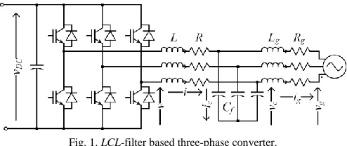
Fig. 1 shows the LCL-filter based three-phase converter. In an industrial converter, the current sensors are integrated on the converter side as they are also used for protection [4]. Hence, in this paper the converter current will be sensed [26]. Neglecting the parasitic resistances in all the LCL-filter elements, the transfer function relating to the converter voltage, v, and the converter current, i, is [6]:
2 2
2 2 1 ) (
) ( ) (
res LC ud
ω + s
z + s Ls = s v
s i = s
G (1)
where zLC
2 =(LgCf)
−1
and the resonance frequency is ωres2=(2πfres)2=(1+Lg/L)zLC2 [6]. The transfer function relating
to the grid current, ig, and the converter voltage, v, is [4]:
2 2
2 1 ) (
) ( ) (
res LC g
gud ω
+ s
z Ls = s v
s i = s
G (2)
A slope of 60 dB/decade for ω>>ωres in (2) will highly attenuate the grid current harmonics. Thus, the switching frequency should be selected larger than ωres in the LCL-filter design stage.
When considering real coils (1) and (2) have finite DC gain equal to the sum of R and Rg, the parasitic converter and grid
[image:2.612.316.563.294.398.2]coil resistances respectively.
Fig. 1. LCL-filter based three-phase converter.
The LCL-filter based converter uses the same digital PI controllers for the current loops as the L-filter based converter [27]. In doing so, the complexity of the control algorithm is not increased by using an LCL-filter. The usual criterion for tuning the PI controllers is the technical optimum [28]. The tuning formulas are given for the L-filter plant with transfer function of first order [28]. The transfer function of the LCL -filter (1) is linear but has elevated order. Thus, an equivalent model for low frequency of the LCL-filter allows using the simple formulas established for the L-filter. This can be used because, as will be shown, the LCL-filter resonance affects only to the region of frequencies much higher than current control bandwidth.
The Padé approximant [29] can be used to obtain the LCL -filter equivalent model for low frequency. The Padé approximant pN, M(x) of a function f(x) consists in a quotient of
two polynomials with numerator degree N and denominator degree M. Taylor series expansion of Padé approximant pN,
M(x) equals to Taylor series expansion of f(x) up to degree
M+N [29]. The Padé approximant pN, M(s) of (1) with N=0 and
g
g
eq eq g g
f g
R + R + s L + L
R + s L = R + R + s R C L + L = s p
1
1 1
2 0,1
(3)
Factor CfRg2 in (3) is negligible when compared to L+Lg as
Rg is one order of magnitude lower than ωfLg, with ωf the
fundamental frequency, and Cf is selected not to decrease
power factor more than 5% [5]. This shows that the equivalent model for low frequency is approximately equivalent to eliminate the capacitor branch in the LCL-filter as was done in [5].
B. Control of the equivalent model for low-frequency Converter control is studied using the space vector notation and an average model in the dq-frame rotating at grid frequency ω [5]-[6],[30]. Fig. 2 shows the inner and faster loops controlling the dq-currents and the outer and slower loop controlling the DC-link voltage [4]. The cascaded control structure for the LCL-filter based converter is exactly the same as that of the L-filter based converter except for the active damping block. The active damping block of Fig. 2 is shown enclosed in the dashed lines and will be explained in the following section.
Fig. 2. Block diagram of the digital control for the LCL-filter based rectifier (the active damping is shown enclosed in dashed lines).
A digital processor performing all control tasks has the sampled measurements as inputs and the PWM gate pulses as outputs. For control modeling purposes, the PWM modulator can be regarded as a zero order hold (ZOH) [31]. Thus, the control plant will be the ZOH equivalent of the transfer function (1) relating to v and i considering the parasitic coil resistances.
The parameters for the digital PI controller according to the technical optimum criterion are [28] (damping factor of dominant pole pair ζlf=0.707 for 4% overshoot):
s eq p
T L K
3
(4)
eq eq i
R
L
T
(5)where Ts is the sampling period. Simple update mode is
used i.e. the sampling of all the measurements is done at the beginning of each PWM period and the update of all the outputs (PWM registers) at the ending [28],[32]. Hence, Ts=Tsw where Tsw is the switching period.
The analysis to obtain (4) and (5) was done in the continuous-time domain by modeling the computational and PWM delays as a first order system with time constant τ=1.5Ts
[28]. This approximation is valid because the attained bandwidth (6) is much lower than the sampling frequency:
eq p bw
L K
(6)In order to avoid interference the resonance frequency ωres
should be selected larger than ωbw in the LCL-filter design
stage [5].
The parameters Req and Leq of the equivalent model for low-
frequency are substituted in (4) and (5) for the digital PI controllers of the current loops in the LCL-filter based converter. Nevertheless, the additional zeros and poles in (1) can make the system unstable if the proper damping is not applied [5].
The digital PI controller for the DC-link voltage is usually adjusted following the symmetrical optimum criterion [28] and taking into account the inner and faster d-current control.
III. ACTIVE DAMPING DESIGN
A. Rationale of the procedure
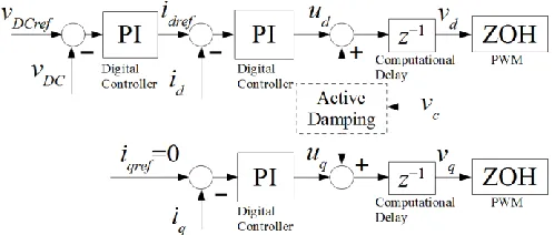
Active damping can be achieved by using a proper feedback state. Thus, the feedback of the current through the LCL-filter capacitors yields resonance damping [10]. Fig. 3 illustrates this concept with the negative feedback of the LCL-filter capacitor current to the converter voltage reference [10],[33]. Assuming ideal feedback, now the transfer function relating to ig and voltage u, converter current PI controller output, results
in:
2 2
2
2 2 1 ) (
) ( ) (
res
damping res res d
LC g
gad
ω + s ω Lω
k + s
z Ls
= s u
s i = s G
(7)
The proportional gain kd is related to the damping factor ζad
as follows:
res d ad
L k
2
[image:3.612.49.298.375.481.2]Unlike the passive damping case, the transfer function (7) does not have a zero that degrades the LCL-filter effectiveness [34]. Hence, as was observed in [6], increasing the gain kd to
increase the damping will not incur increasing the grid current ripple. According to (8) the gain kd will have the same order of
magnitude as twice the inverter coil impedance at the resonant frequency 2Lωres since 0<ζad<1. The transfer function relating
to i and u is [34]:
[image:4.612.50.295.159.320.2]
2 2 2 2 2 2 1 ) ( ) ( ) ( res damping res res d LC ad ω + s ω Lω k + s z s Ls = s u s i = s G (9)Fig. 3. LCL-filter capacitor current feedback to obtain damping.
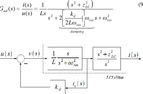
In order to avoid the use of new current sensors [34]-[35] the LCL-filter capacitor current ic can be estimated from the
derivative of the LCL-filter capacitor voltage vc [33], see Fig.
4, as follows:
=k C sv i s
H d f
c c
[image:4.612.318.563.304.397.2]d (10)
Fig. 4. Feedback of the capacitor voltage derivative to obtain damping in the
LCL-filter.
B. Minimum gain for stability
Considering the open-loop transfer function of the converter current control in the continuous-time domain:
) ( ) ( ) ( )
(s G s G sG s
Gadol PI delays ad (11)
where Gad(s) is the plant (9), Gdelays(s) is a pure delay s
Ts
e1.5 modeling the computational and PWM delays, and finally GPI(s) is the PI controller tuned according to (4) and
(5). The frequency that corresponds to −180º phase-shift for the open-loop transfer function is near the resonant frequency [6], [12]. The resonant peak should be below unity (0 dB) [12]
for the current control to be stable by achieving a positive gain margin. Thus, the minimum kdmin (considered as a variable
parameter) for stability can be obtained by equating the open-loop transfer function to unity (0 dB) at the resonance frequency (s=jωres):
1 ) ( ) ( ) ( ) ( res
res PI delays ad s j
j s
adol s G s G s G s
G
(12)
Substituting and solving in (12) and neglecting the smaller terms results in:
s g dmin T L k 3 1 (13)
C.Lead-lag network tuning
[image:4.612.51.293.409.533.2]A perfect differentiator for the capacitor voltage would amplify the measurement signal noise too much and thus, a lead-lag network should be used instead, see Fig. 5.
Fig. 5. Feedback of LCL-filter capacitor voltage filtered by a lead-lag network to obtain damping.
A proper form for the lead-lag network consists of the following transfer function:
max f max f max f d ll ω + s k ω k + s ω C k = s
H ( ) with
max max f + = k
sin 1 sin1 (14)
where ωmax=2πfmax is the frequency for the maximum phase
shift φmax (|φmax|<90º), see Fig. 6.
The lead-lag network behaves as a differentiator at frequencies around the resonance frequency, where damping is necessary, by selecting φmax close to 90º and in addition:
res max=ω
ω (15)
By doing this, (14) has for ω=ωres an amplitude equal to
kdCωres a phase close to 90º with zero slope just like in (10).
The amplitude slope of (14) for ω=ωres is:
2 2 1 1 ) ( f f f d ll k k C k = d j H d res
(16)equal to kdCf, see Fig. 6, if kf<1 (0<φmax<90º). Indeed, kf
should be as small as possible (φmax as close to 90º as
possible). If kf>1 (−90º<φmax<0) the amplitude slopes of (14)
and (10) have different signs for ω=ωres, see Fig. 6, and the
lead-lag network no longer behaves as a differentiator.
Fig. 6. Bode diagram of the perfect differentiator in (10) and the lead-lag network in (14) for kf>1 and kf<1.
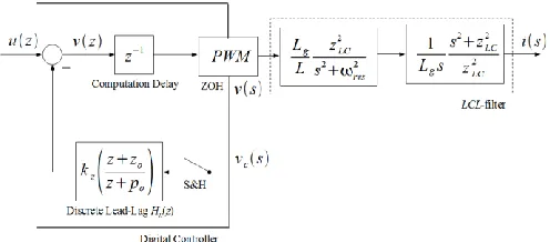
The lead-lag network for active damping is implemented in the digital controller, see Fig. 7. The synchronous sampling of the capacitor voltage requires symmetry in the PWM pulse to obtain a ripple free waveform and so simple update mode (Ts=Tsw) is only used.
Fig. 7. Implementation of the lead-lag network for active damping in the digital controller.
The digital implementation [36]-[37] incorporates lag phase shifts due to the presence of the computational delay and the PWM. To calculate these lag phase shifts the computational delay is modeled as a pure delay of Ts and the PWM,
equivalent to a ZOH, as a pure delay of 0.5Ts [28]. This
approximation results in adequate accuracy for frequencies much lower than fs.
The discrete lead-lag network must behave as a perfect differentiator around the resonance frequency. Hence, the phase shift at the resonance frequency must lead 90º once the phase shifts due to the PWM and the computational delays are compensated:
delays nal computatio and PWM
2
360
1.5
º
90
max
T
s res
(17)In order to preserve the phase and amplitude characteristics at the resonance frequency (14) must be discretisized by using the bilinear transformation (Tustin method) with pre-warping at ω=ωres [6], [39]. The discrete equivalent of (14) has the
form kz(z+zo)/(z+po) with kz a gain, zo a zero and po a pole.
The sampling frequency to get kf<1, which corresponds to
0<φmax<90º (14), is 1.5fres<fs<2fres according to (17). However,
the digital control requires the resonance frequency to be lower than the Nyquist frequency so fs>2fres [39]. If the gain kd
in (14) is selected negative, a phase lag of 180º must be added in (17). This results in kf<1, 0<φmax<90º (14), for 3fres<fs<6fres
(17), which fulfills the previous condition fs>2fres. A negative
gain kd in (14) is coherent with the original formulation of the
lead-lag method [12], which used positive feedback of the capacitor voltage filtered by the lead-lag network. The switching frequency fsw should be selected as low as possible
to reduce the switching losses [38]. As fsw=fs then fs should be
selected as close to 3fres as possible. It is not possibleto make
fs=3fresas this corresponds to φmax=90º and (14) would result in
a pure derivative. A practical upper limit is φmax=80º [6],
corresponding to fs=3.2fres (17). In addition, there is a lower
limit φmax=70º, corresponding to fs=3.4fres (17), to make (16)
close (>90%) to the perfect differentiator slope. Hence, the frequency ratio should be selected in the following range:
4 . 3 2 .
3
res s
f
f (18)
The approximation for the computational and PWM delays used in (17) is valid for the ratios according to (18). Indeed, the achieved bandwidth for the current control according to (6) for the ratio (18) is approximately fbw≈fres/5. Hence, the
resonance does not affect very much to the current control that can be safely tuned using the equivalent model for low frequency.
Root locus analysis in the z-plane, considering the discrete nature of the employed digital control, is used to select the gain kd that results in an adequate damping of the closed-loop
poles. The gain kd cannot be arbitrarily increased to get a very
high damping as the system becomes unstable [6].
D. Equivalent model for low-frequency
At low and high frequencies where damping is not necessary, ω<<kfωmax and ω>>ωmax/kf, (14) behaves as a
constant, HllDC=kdCfωmaxkf and kdCfωmax/kf respectively,
[image:5.612.47.297.125.283.2] [image:5.612.49.297.394.503.2]where the passive damping is not necessary [35], [38].
The equivalent model for low frequency of the LCL-filter including the lead-lag network by using the Padé approximant results in:
DC
DC DC
2 DC
1
1 1
1
ll g
f f res
ll g ll g f ll g eq
H L L
k k H R H R C H L L L
(19)
1 llDC
g
eq R R H
R (20)
The equivalent resistance and inductance from (19) and (20) are to be substituted in (4) and (5) for the digital PI controller of the converter current.
E. Overshoot reduction
The gain Kp in (4) was selected only having into account the
equivalent model for low frequency. The high frequency behavior of the LCL-filter and the equivalent notch filter produces higher overshoot to the step input than the expected 4% [6]. Half Kp in (4) would make the closed-loop dominant
poles critically damped (ζlf=1) and the only present overshoot
would be due to the high frequency dynamics. So if overshoot is not acceptable Kp should be reduced, but not as much as
halving (4), until obtaining acceptable overshoot. Nevertheless, this solution would be at the expense of reducing the overall bandwidth according to (6).
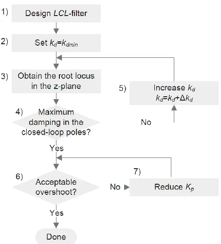
F. Design flow
Fig. 8 shows the step-by-step procedure for the active damping design of the LCL-filter based rectifier.
Fig. 8. Design flow for the active damping design of the LCL-filter based
rectifier.
For the step 1) the guidelines proposed in [4],[5] can be used. The switching frequency is selected according to (18). The gain kd with the poles entering in the unit circle of the root
locus (minimum value for stability) will be near kdmin (13),
initial value of the step 2). Several times (9) can be used as the maximum kd. The digital PI controllers are tuned according to
(4),(5) by using the equivalent model for low frequency (19),(20). In the steps 3), 4) and 5) the gain kd is progressively
increased until obtaining the optimum value corresponding to the maximum damping of the closed-loop poles.
The maximum value is detected by observing a reduction in the damping for an increase in the gain kd. This simple
optimization algorithm is known as hill-climbing [40]. The increment length for the step 5) is initially selected according to (8) Δkd=2LωresΔζad by considering increments in Δζad=1%.
A shorter increment Δζad can be selected for greater accuracy
at the expense of a larger computation period. These steps are automated by using a scripting language for numerical calculations such as Matlab [29],[39].
IV. SIMULATION RESULTS
Simulation models have been built using Matlab and Simulink. The LCL-filter data are from [5] complying step 1) in the proposed design flows: Lg=5 mH, L=3 mH, and Cf=2.2
μF so fres=2478 Hz. Parasitic coil resistances are chosen to be
one order of magnitude less than the coil impedance at fundamental frequency. The converter data are: rated power Pnom=4.1 kW, Vnom=380 V (rms phase-to-phase), fundamental
frequency ff=50 Hz, DC-link voltage VDC=700 V, DC-link
current IDC=5.5 A (simulated as a simple DC-link load
resistor), and DC-link capacitor CDC=500 μF. Current control
loops were equipped with anti-windup mechanisms. The adopted PWM modulation strategy is SVM. A digital dq-PLL [32] is used for AC voltage synchronization. Voltage sensors are located across the LCL-filter capacitor branch for active damping. Simple update mode is used so Ts=Tsw. The
simulations are ideal without any non-linear effect (ideal switches, no dead time, no coil saturation and perfect sinusoidal grid voltage).
Active damping according to the proposed design flow is as follows:
Step 1) the LCL-filter data were selected from the reference [5]. The selected switching frequency is 8 kHz according to (18), this corresponds to φmax=77.3º according to (14).
Step 2) the optimization algorithm starts for kd=kdmin. The
estimation (13) for the minimum kd to achieve stability is quite
accurate for higher frequencies. This was expected since deducing (13) was based on assuming high switching frequencies. For fsw=8 kHz the calculated minimum gain
results kdmin=13.35 and by substituting in (13) kdmin=13.35 Fig.
9 shows the root locus in z-plane of the converter current control for increasing gains kd. It can be seen that the
[image:6.612.57.284.472.723.2]dominant pole pair follows the lines of constant damping factor ζlf=0.707 by considering the Padé approximant for the
equivalent model according to (19) and (20).
Steps 3), 4) and 5) the gain kd is progressively increased
until obtaining the maximum damping in the closed-loop poles for kd =27, corresponding to ζcl>0.15. The optimization
algorithm stops at reaching the optimum kd =27.
Notwithstanding, Fig. 9 shows how the system starts to change its dynamics for kd>27 and tends again to be unstable.
Closed-loop poles leave the unit circle for kd>46 and the system
becomes unstable.
Step 6) and 7) the resulting overshoot is 13.5%, more than the expected 4% if not allowable Kp should be reduced.
Halving the proportional gain Kp reduces the overshoot to
zero. Decreasing the gain to 85% Kp reduces the overshoot to
below 4% at the expense of decreasing the bandwidth according to (6).
Fig. 9. Closed-loop poles in the z-plane of the converter current control by varying kd for the active damping case.
Grid currents obtained from simulation for kd=27 resulted in
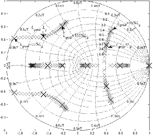
very clean waveforms with THD=0.6%. Fig. 10 shows the root locus in z-plane of the converter current control by varying the grid inductance due to variations in the line impedance. The real grid impedance Lgrid varies between
50-150% of the considered inductance value Lg. It can be seen
that increasing values of the real grid inductance result increasing damping of the closed-loop poles and vice versa. This was expected from (8) as the achieved damping factor for the calculated kd increases as the resonance frequency
decreases and vice versa.
It can also be seen that for decrements in the real grid inductance Lgreal=55%Lg with Δωres=14%ωres the system
enters instability but for increments Lgreal=155%Lg with only
Δωres=–7%ωres the system remains stable. This is because the
LCL-filter is designed to have Lg/L>1 [4] so elevated
increments in the grid inductance are necessary to significantly reduce the resonance frequency (negative Δωres).
Indeed, as the resonance frequency separates from the considered one for (14), the lead-lag network detaches from its behavior as differentiator and the active damping loses its efficacy. Thus, the active damping procedure is more sensitive to decrements in the real grid inductance and in case of uncertainty; it would be advisable to underestimate Lg. Finally,
the PI controllers will result in higher overshoots (less damping of the dominant poles) for the decreasing values of the real grid inductance and vice versa.
Fig. 10. Closed-loop poles in the z-plane of the converter current control by varying the grid inductancefor the active damping case.
V. EXPERIMENTAL RESULTS
One of the advantages of Simulink is the capability to generate code for the implantation (DSP [41] or FPGA [42]) directly from the block diagrams [43]. This feature eliminates the tedious and error prone task of hand coding the control algorithm. However, the proposed procedures use the standard nested structure of Fig. 2 for the rectifier control [32] and so all the already available code can be reutilized. Therefore, the only necessary new code is for active damping block of Fig. 2. Due to its superior numerical properties, it is recommended to use the direct form II transposed structure [44] to implement the discrete lag network. The code for the discrete lead-lag networks is incorporated to the PWM interrupt service routine [32] and so its execution is scheduled in the same slot [45] as the current control loop.
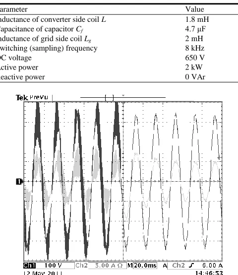
The experimental setup, see Fig. 11, consists of a 2.2 kW Danfoss FC302 converter connected to the grid through an isolation transformer and supplied by Delta Elektronika power supplies. The setup parameters are shown in Table I.
The resonance frequency is fres=2385 Hz and the maximum
angle is φmax=71º according to (14). The maximum damping
for closed-loop poles results in kd=13. The measured
[image:7.612.316.561.165.382.2] [image:7.612.51.294.262.473.2]upon the connection of the lead-lag network are shown in Fig. 12. Thus, the experiment confirms the stability and correctness of the proposed tuning procedure.
Fig. 11. The laboratory setup: a) photo of setup; b) hardware wiring diagram.
TABLE I.PARAMETERS OF THE EXPERIMENTAL SET-UP.
Parameter Value
Inductance of converter side coil L 1.8 mH
Capacitance of capacitor Cf 4.7 μF
Inductance of grid side coil Lg 2 mH
Switching (sampling) frequency 8 kHz
DC voltage 650 V
Active power 2 kW
Reactive power 0 VAr
VI. CONCLUSION
This paper is intended as a guide to systematic design of the lead-lag network method for active damping in LCL-filter based three phase converters. The capacitor current feedback to voltage references constitutes the rationale of the method. This allows explaining the parameter tuning by means of unsophisticated linear techniques. Root locus analysis in z -plane is necessary to assess stability in selecting the lead-lag network gain. A simple optimization algorithm is used to select lead-lag network corresponding to the maximum damping in the closed-loop poles. Simulation and experiments confirm the validity of the proposed design flow. Hence, the parameters of the lead-lag network method for active damping are calculated without recurring to trial-and-error iterations. This procedure is limited to simple update mode with the
narrow range for the switching frequency. Future research should study the underlying notch nature of the lead-lag network method to tune the notch filter directly inserted in the controller path.
REFERENCES
[1] M. Liserre, T. Sauter and J.Y. Hung: "Future Energy Systems: Integrating Renewable Energy Sources into the Smart Power Grid Through Industrial. Electronics," in IEEE Ind. Electron. Mag., vol.4, no.1, pp.18-37, March 2010
[2] J.M. Guerrero, F. Blaabjerg, T. Zhelev, K. Hemmes, E. Monmasson, S. Jemei, M.P. Comech, R. Granadino and J.I. Frau: "Distributed Generation: Toward a New Energy Paradigm," in Ind. Electron. Magazine, IEEE , vol.4, no.1, pp.52-64, March 2010
[3] W. Su, H. R. Eichi, W. Zeng and M.-Y. Chow: "A Survey on the Electrification of Transportation in a Smart Grid Environment ," in IEEE Trans. on Ind. Informat., vol. 8, no. 1, pp. 1-10, Feb 2012
[4] M. Liserre, F. Blaabjerg and A. Dell'Aquila: "Step-by-step design procedure for a grid-connected three-phase PWM voltage source converter," in int. J. of Electron., vol. 91, no. 8, pp. 445-460, August 2004
[5] M. Liserre, F. Blaabjerg and S. Hansen: "Design and control of an
LCL-filter-based three-phase active rectifier," in IEEE Trans. on Ind. Applicat., vol.41, no.5, pp. 1281- 1291, Sept.-Oct. 2005
[6] M. Liserre, A. Dell'Aquila and F. Blaabjerg: "Stability improvements of an LCL-filter based three-phase active rectifier," in 2002 IEEE 33rd Annu. Power Electron. Specialists Conf., 2002. PESC’02. Vol. 3, pp. 1195- 1201, 2002
[7] P. Channegowda and V. John: "Filter Optimization for Grid Interactive Voltage Source Inverters," in IEEE Trans. on Ind. Electron., vol. 57, no. 12, pp. 4106-4114, December 2010
[8] . Pe a- l ola . iserre F. laab erg . Sebasti n, J. Dannehl and F.W. Fuchs: "Analysis of the Passive Damping Losses in LCL-Filter-Based Grid Converters," in IEEE Trans. on Power Electron., vol.28, no.6, pp.2642,2646, June 2013
[9] A. M. Hava, T. A. Lipo and W. L. Erdman: "Utility interface issues for line connected PWM voltage source converters: a comparative study," in
Proc. APEC'95, Mar. 1995, pp. 125-132
[10] J. Dannehl, F.W. Fuchs, S. Hansen and P.B. Thøgersen: "Investigation of Active Damping Approaches for PI-Based Current Control of Grid-Connected Pulse Width Modulation Converters With LCL Filters," in
IEEE Trans. on Ind. Applicat., vol.46, no.4, pp.1509-1517, July-Aug. 2010
[11] Yi Tang, Poh Chiang Loh, Peng Wang, Fook Hoong Choo, Feng Gao and F. Blaabjerg: "Generalized Design of High Performance Shunt Active Power Filter with Output LCL Filter," in IEEE Trans. Ind. Electron., vol.59, pp.1443-1452. March 2012
[12] V. Blasko and V. Kaura: "A novel control to actively damp resonance in put LC filter of a three-phase voltage source converter," in IEEE Trans. onInd. Applicat., vol.33, no.2, pp.542-550, Mar/Apr 1997
[13] M. Malinowski and S. Bernet: "A Simple Voltage Sensorless Active Damping Scheme for Three-Phase PWM Converters With an LCL Filter," in IEEE Trans. on Ind. Electron., vol.55, no.4, pp.1876-1880, April 2008
[14] P. A. Dahono: "A control method to damp oscillation in the input LC filter of AC-DC PWM converters," in Proc. PESC’02, June 2002, pp. 1630–1635
[15] J. He and Y. Li: "Generalized Closed-Loop Control (GCC) Schemes with Embedded Virtual Impedances for Voltage Source Converters with LC or LCL Filters," in IEEE Trans. Power Electron., vol: PP, pp.1-1, Sep. 2011
[16] Jinwei He and Yun Wei Li: "Analysis, Design, and Implementation of Virtual Impedance for Power Electronics Interfaced Distributed Generation," in IEEE Trans. Ind. Applications, vol.47, pp. 2525-2538. Nov.-Dec. 2011
[17] E.J. Bueno, F. Espinosa, F.J. Rodríguez, J. Ureña and S. Cóbreces: "Current Control of Voltage Source Converters connected to the grid through an LCL-filter," in 35 th Annu. IEEE Power Electron. Specialists Conf. (PESC’04). achen, Germany, 2004. pp. 68 – 73
Fig. 12. Measured capacitor voltage (100 V/div) and grid current (5 A/div) upon the connection of the lead-lag network.
[image:8.612.55.295.237.514.2][18] M. Bojrup: Advanced Control of Active Filters in a Battery Charger Application, Licentiate Thesis TEIE-1021. ISBN: 91-88934-13-6. Dept. of Ind. Elect. Eng. and Automat. Lund Institute of Technology. 1999 [19] M. Liserre, . Dell’ quilla and F. laab erg: "Genetic algorithm based
design of the active damping for a LCL-filter three-phase active rectifier," in IEEE Trans. onPower Electron., vol.19, no.1, pp. 234-240, Jan 2003
[20] J. Dannehl, M. Liserre, F. Fuchs: "Filter-based Active Damping of Voltage Source Converters with LCL-filter," in IEEE Trans. onInd. Electron., vol.58, no.8, pp. 3623-3633, Aug. 2011
[21] K. Jalili and S. Bernet: "Design of LCL filters of active-front-end two-level voltage-source converters," in IEEE Trans. on Ind. Electron., vol. 56, no. 5, pp. 1674-1689, May-2009
[22] J.L. Agorreta, M. Borrega, J. López And L.Marroyo: "Modeling and control of n-paralleled grid-connected inverters with lcl filter coupled due to grid impedance in PV plants," in IEEE Trans. on Power Electron., vol. 26, no. 3, pp. 770-785, March 2011
[23] W. Zhao and G. Chen:"Comparison of active and passive damping methods for application in high power active power filter with LCL-filter," in Conf. on Sustainable Power Generation and Supply, 2009. pp. 1-6, 6-7 April 2009
[24] C. Liu, X. Zhang, L. Tan, T. LiHua, F. Liu:"A novel control strategy of LCL-VSC based on notch concept," in 2nd IEEE Int Symp. on PEDG, pp.
343 - 346, 16-18 June 2010
[25] S.Y. Yang, X. Zhang, C.W. Zhang, Z. Xie:"Study on active damping methods for voltage source converter with LCL input filter", in IEEE 6th IPEMC '09, pp. 975 - 979, 17-20 May 2009
[26] Jinjun Yin, Shanxu Duan and Bangyin Liu: "Stability Analysis of Grid-Connected Inverter With LCL Filter Adopting a Digital Single-Loop Controller With Inherent Damping Characteristic," in IEEE Trans. on Ind. Informat., vol.9, no.2, pp.1104,1112, May 2013
[27] J. Dannehl, C. Wessels and F.W. Fuchs: "Limitations of Voltage-Oriented PI Current Control of Grid-Connected PWM Rectifiers With LCL Filters," in IEEE Trans. on Ind. Electron., vol.56, no.2, pp.380-388, Feb. 2009
[28] V. Blasko and V. Kaura: "A new mathematical model and control of a three-phase AC-DC voltage source converter," in IEEE Trans. onPower Electron., vol.12, no.1, pp.116-123, Jan 1997
[29] W.Y. Yang, W. Cao, T.S. Chung and J. Morris: Applied Numerical Methods Using Matlab (1st edition), Wiley-Interscience, May 2005. ISBN: 0-471-69833-3
[30] R. Sebastian and R. Peña-Alzola: "Simulation of an isolated Wind Diesel System with battery energy storage," in Elect. Power Systems Research, vol.81, Issue 2, February 2011, pp.677-686
[31] S. Buso and P. Mattavelli: Digital Control in Power Electron., Morgan and Claypool Publishers, 2006. ISBN: 1-598-29112-2
[32] M.P. Kazmierkowski, M. Jasinski and G. Wrona: "DSP-Based Control of Grid-Connected Power Converters Operating Under Grid Distortions," in IEEE Trans. on Ind. Informat., vol. 7, no. 2, pp. 204-211, May 2011
[33] W. Gullvik, L. Norum and R. Nilsen: "Active damping of resonance oscillations in LCL-filters based on virtual flux and virtual resistor," in
European Conf. onPower Electron. and Applicat., pp.1-10, 2-5 Sept. 2007
[34] C.P. Dick, S. Richter, M. Rosekeit, J. Rolink and R.W. De Doncker: "Active damping of LCL resonance with minimum sensor effort by means of a digital infinite impulse response filter," in 2007 European Conf. onPower Electron. and Applicat., pp.1-8, 2-5 Sept. 2007 [35] Aiguo Xu, Zhiying Xu, Shaojun Xie and Mengshu Zou: "Study on
dual-loop grid current control scheme for grid-connected inverter with an LCL-filter," in 4th IEEE Conf. on Ind. Electron. and Applicat., 2009. ICIEA 2009, pp.3200-3203, 25-27 May 2009
[36] C. Buccella, C. Cecati, H. Latafat: "Digital Control of Power Converters—A Survey," in IEEE Trans. Ind. Informat., vol.8, no.3, pp.437,447, Aug. 2012
[37] C. Sepulveda, J. Munoz, J. Espinoza, M. Figueroa and F.C. Baier: "FPGA v/s DSP Performance Comparison for a VSC-based STATCOM Control Application," in IEEE Trans. Ind. Informat., vol.PP, no.99, pp.1,1
[38] A.A. Rockhill, M. Liserre, R. Teodorescu and P. Rodriguez: "Grid-Filter Design for a Multimegawatt Medium-Voltage Voltage-Source Inverter," in IEEE Trans. on Ind. Electron., vol.58, no.4, pp.1205-1217, April 2011
[39] G.F. Franklin, J.D. Powell and M.L. Workman: Digital Control of Dynamic Systems (3rd Edition), Addison Wesley Longman, 1997. ISBN:
0-201-82054-4
[40] J.A. Storer: An Introduction to Data Structures and Algorithms, Birkhäuser Boston, 2001, ISBN-10: 0-817-64253-6
[41] A. Malinowski and Hao Yu: "Comparison of Embedded System Design for Ind. Applications," in IEEE Trans. on Ind. Informat., vol. 7, no. 2, pp. 244-254, May 2011
[42] E. Monmasson, L. Idkhajine, M.N. Cirstea, I. Bahri, A. Tisan and M.W. Naouar: "FPGAs in Control Applications," in IEEE Trans. on Ind. Informat., vol. 7, no. 2, pp. 224-243, May 2011
[43] M. Di Natale, Liangpeng Guo, Haibo Zeng and A. Sangiovanni-Vincentelli: "Synthesis of Multitask Implementations of Simulink Models With Minimum Delays," in IEEE Trans. on Ind. Informat., vol. 6, no. 4, pp. 637-651, Nov 2010
[44] L. Harnefors: "Implementation of resonant controllers and filters in fixed-point arithmetic," in IEEE Trans. on Ind. Electron., vol. 56, no. 4, pp. 1273-1281, April 2009