International Journal of Innovative Technology and Exploring Engineering (IJITEE) ISSN: 2278-3075, Volume-8 Issue-9, July 2019
Abstract: Selecting an appropriate substrate material for the design of microstrip patch antenna for various applications is a very important step in antenna design. This paper presents a work of various substrates materials used for the design of low cost inset feed rectangular microstrip antenna for WLAN, WiMax, LTE, C-band and X-band applications. The substrates used are FR-4 epoxy, foam, polyethylene terephthalate (PET) and polydimethylsiloxane (PDMS). The antennas were designed, optimized and simulated using HFSS 15.0. Return loss, voltage standing wave ratio and gain analysis is carried out for these antennas. The measurement of reflection coefficient of the fabricated antennas is done using Agilent PNA-L series vector network analyzer. The simulated and measured results are well in agreement. The analysis show that antenna with foam substrate offers the lowest return loss of - 41.28 dB. Larger bandwidth and gain of 4.38 dB is observed with PET substrate.
Index terms- Patch antenna, inset feed, substrates.
I. INTRODUCTION
In wireless communication system antenna design is one the important challenge. Recently, in many papers, low cost materials are been considered as more likely materials for the antennas to participate for improving the flexibility factor [1]. The expanding utilization of wireless communication frameworks requires the antenna for various frameworks with properties like multiple resonant frequencies, compact, flexible. Rectangular microstrip patch antenna with inset feed technique is proposed in this paper. Inset feed technique provides better impedance matching as compared to simple line transmission technique [2,3]. The patch and ground are made of conductive material and the substrate is in between these two layers. There are number of different substrates that can be utilized for design of an antenna. Before designing the antenna, the dielectric constant, frequency and height of the substrate should be well known. The dielectric constant of substrate is usually between range 2.2 ≤ Ԑr ≤ 12[4].
In the investigation of work, a tag antenna structured on a PET substrate and actualized by inkjet printing utilizing a conductive ink. It works in the whole UHF frequency band used for RFID (from 860 to 960 MHz). To achieve lager bandwidth the antenna is proposed without ground plane [5]. Next paper targets wearable application, a planar patch
Revised Manuscript Received on June 08, 2019.
Pooja Siriya, Department of Electronics Engineering, Shri Ramdeobaba College of Engineering and Management, Nagpur, India.
Dr. J. A. Shrawankar, Associate Professor, Department of Electronics Design Technology, Shri Ramdeobaba College of Engineering and Management, Nagpur, India.
Dr. Suresh Balpande, Assistant Professor, Department of Electronics Engineering, Shri Ramdeobaba College of Engineering and Management,
antenna is considered more practical than other types of antennas. The design of the patch antenna is fairly simple and can be further simplify the measurement using a microstrip feed. Bending effect is also investigated as antenna bending is very common in most personal portable device applications. A flexible SU-8/PDMS-based antenna is presented in [6]. Another paper reports a planar four-element array of U-slot patches with its measured results. The patches are designed using proximity coupling by a microstrip line feed with ԓ-shaped stubs. Here, dielectric layer is of foam which is very light in weight [7]. The next paper targets a microstrip patch array antenna which is suitable for military application. To reduce mutual coupling defected ground structure is used for optimizing results [8].
The paper is further organized as follows, in section II Design method and parameter is discussed, simulated and measured results of antennas on different substrates is presented in section III, result and discussion is in section IV followed by conclusion in section V.
II. DESIGN METHOD AND PARAMETER
In this section the method of dielectric constant measurement, the antenna geometry and simulation methodology of the antenna is illustrated.
A. Dielectric Constant Measurement
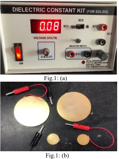
As we are aiming for low-cost substrate material which can be used for various applications such as WLAN, WiMax LTE, C-band and X-band, the materials selected are FR-4 epoxy, PET, PDMS and foam. These materials are easily available and also can be manufactured at low price. Here materials are developed in our laboratory and then its dielectric constant is measured. The properties of a patch antenna are largely determined by the properties of the substrate used for the design. Thus, for the design an antenna or the other planar circuits, the effective relative permittivity of the substrate must be known with a high degree of accuracy. The properties of a patch antenna are to a great extent determined by the properties of the substrate utilized for the design [9]. Dielectric constant is measured as the ratio of the capacitance C of an electric condenser filled with the dielectric to the capacitance Co of the evacuated condenser. The Fig.1 (a) below shows the setup of dielectric constant measurement and the Fig.1 (b) shows the gold-plated brass discs between which substrate material is placed. The discs are of two different sizes 75mm and 25mm depending upon the material.
Design And Development of Inset Feed
Microstrip Patch Antennas using Various
Substrates
Fig.1: (a)
Fig.1: (b)
Fig 1: (a) Dielectric constant kit. (b) Gold plated brass discs of electric condenser
To know the exact dielectric constant of the material a dielectric constant kit has been used. The materials (FR4-epoxy, PET, PDMS and foam) dielectric constant is determined using this device. In this the substrate material is placed between the two conductive material plates. LC circuit is used to determine the capacitance of the dielectric cell and hence the dielectric constant. A couple of precautionary measures are taken like the substrate material surface must be with no roughness and no air gap is there in the middle and least pressure should be applied on materials. The measured dielectric constant of the materials is listed in the table 1.
Sr. No.
Materials Dielectric
constant
1. FR-4 epoxy 4.4
2. Foam 1.31
3. Polyethylene terephthalate (PET) 2.5
[image:2.595.69.261.49.305.2]4. Polydimethylsiloxane (PDMS) 3.11
Table 1: Measured dielectric constant values
Let us move to the next section in which the actual simulated design structure of the microstrip patch antenna is shown.
B. Antenna Geometry
Rectangular microstrip patch antenna with inset feed technique is easy to design and offer very good impedance matching and larger radiation efficiency compared to simple line transmission technique and coaxial feed technique. Fig 2 (a), (b), (c) illustrates top view, bottom view and side view along with the dimensions used in simulation. Cut size (g) and depth of feed line (Yo) optimize the impedance matching for better performance of the antenna.
Fig.2: (a) Top View
Fig.2: (b) Back View
Fig.2: (c)Side View
Fig 2: (a) Top view, (b) Back view & (c) Side view of the antenna
Here the design structure of antenna is seen. In the next section the formulas used to calculate the dimensions are shown.
C. Design Formulae
Using following formulas, the dimensions of the antennas are calculated [10].
The length (L) and width (W) of the patch is calculated using equation (1) and (2).
- (1)
Where,
c= Speed of light in vacuum/free-space/air fc = Resonating frequency
Ԑr = Dielectric constant of substrate material
- (2)
Where,
h = Height of the substrate material
[image:2.595.325.530.55.390.2] [image:2.595.50.290.481.593.2]International Journal of Innovative Technology and Exploring Engineering (IJITEE) ISSN: 2278-3075, Volume-8 Issue-9, July 2019
- (3)
For optimizing better results the dimensions of the ground plane are selected as,
Lg = 2L -(4)
Wg = 2W -(5)
The transmission feed line width (wf) is calculated by the equation (6).
-(6)
Where,
)
Where,
Zo = Characteristic impedance of feed line
The cutsize(g) is optimized according to [2] & [3]. By varying the cutsize dimension an exact point is selected where minimum reflection coefficient is obtained. The study shows that as the cutsize decreases the S11 parameter also decreases.
III. SIMULATED AND MEASURED RESULTS OF ANTENNAS ON DIFFERENT SUBSTRATES In this section simulated and measured frequency response of antennas on different substrate materials are shown. S11 plots are presented with the actual image of antenna design. As mentioned earlier testing is done with VNA.
A. Design of rectangular microstrip antenna on FR4-epoxy substrate
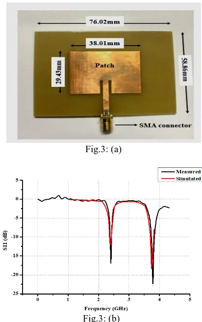
In this design FR-4 epoxy is used as a substrate material. The ground and patch are made of copper. FR-4 epoxy is a widely used and easily available substrate material. It is composed of woven fiberglass cloth with an epoxy resin that is flame resistant. This type of material is not flexible in nature therefore it cannot be used for wearable applications. A double-sided FR-4 sheet is selected with copper as a conducting material. Dielectric constant measured is Ԑr=4.4 and substrate thickness h=1.59mm. The length (L), width (W) of the patch and other parameters are calculated using formulas mentioned in section II. For the inset feed length (Yo) variation in size of its length is done. By doing this better result are obtained. Yo= 8.95mm is selected and transmission line width 3.04mm is calculated. In general, the feed line and ground plane of the microstrip patch antenna fabricated on the printed circuit board (PCB) substrate are connected by soldering with an SMA connector in order to conduct the measurement. The actual fabricated antenna is shown in Fig. 3 (a). The simulated and measured result is shown in Fig. 3 (b). Antenna with FR-4 epoxy substrate exhibits S11 of -17.01dB at frequency of 2.4 GHz and S11 of -23.50 dB at frequency of 3.7 GHz. The simulated gain obtained is 3.73 dB. This antenna is suitable for WLAN, LTE and WiMax applications.
Fig.3: (a)
Fig.3: (b)
Fig. 3: (a) Antenna on FR-4 epoxy substrate. (b) Simulated and measured result of FR-4 epoxy substrate
B. Design of rectangular microstrip antenna on Foam substrate
Foam have higher dimensional stability, low moisture absorption and higher strength. It is light in weight and of unbending structure. The height of substrate h=2.38mm, dielectric constant measured is Ԑr=1.31 and transmission feedline width is 10.75mm. Yo is optimized to 16mm for better impedance matching. Foam is coated with silver ink of thickness 0.035mm on patch and ground. The simulated gain is obtained to be 2.62dB. Fig. 4 (a) shows the fabricated antenna and the simulated and measured S11 parameter analysis is given in Fig 4(b). The measured S11 parameter of this antenna is -41.28dB at a frequency of 4.55GHz. Fabricated antenna is suitable for C-band applications with band width of 500MHz.
[image:3.595.321.527.48.376.2]
Fig.4: (b)
Fig 4: (a) Antenna on Foam substrate. (b) Simulated and measured result of Foam substrate
C. Design of microstrip antenna on PET substrate PET is a rigid, lightweight, dimensionally stable and a moisture barrier material. But this material is not flexible in nature. Here a transparent PET sheet is used with a dielectric constant obtained to be 2.5. The height of the substrate is 1.3mm, Yo= 10mm, transmission feedline width =3.7mm. Silver ink of thickness 0.035mm is coated on patch and ground as conducting material. The gain of this antenna is 4.38dB. The actual image of fabricated antenna is shown in Fig.5 (a). The simulated and measured S11 parameter is plotted in Fig.5(b). The measured S11 parameter for PET substrate is -22.40 at frequency of 9.21 GHz. The simulated gain is 4.38 dB. This antenna has application in X-band with large bandwidth.
Fig.5: (a)
Fig.5: (b)
Fig 5: (a) Antenna on PET substrate. (b) Simulated and measured result of PET substrate
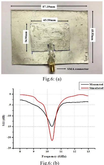
D. Design of microstrip antenna on PDMS substrate PDMS is transparent and flexible material can be used for on – body and off - body application. PDMS substrate of thickness 1.5mm. To make a flexible material 9.2 grams of silicon elastomer and 0.9 curing agent has been used. The PDMS substrate for the proposed antenna is prepared as per the procedure given in [11,12,13]. Dielectric constant is measured as described in section II and found to be 2.85, PDMS substrate is coated with silver ink of thickness 0.035mm as patch and ground conductor, cut size = 1.5mm, feed line width= 3.68mm, Yo is optimized to 7 mm. The gain of this antenna is 1.66 dB. The simulated and measured S11 parameter is shown in Fig.6 (b). The antenna gives S11 parameter of -14.59dB at frequency of 10.37GHz. This antenna is suitable for X-band applications.
Fig.6: (a)
Fig.6: (b)
Fig 6: (a) Antenna on PDMS substrate. (b) Simulated and measured result of PDMS substrate
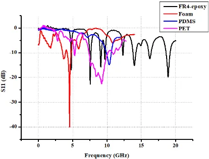
IV. RESULT AND DISCUSSION
[image:4.595.68.268.51.213.2] [image:4.595.326.532.241.567.2] [image:4.595.75.266.435.734.2]International Journal of Innovative Technology and Exploring Engineering (IJITEE) ISSN: 2278-3075, Volume-8 Issue-9, July 2019
[image:5.595.64.271.50.208.2]
Fig 7: Measured result of all antennas
V. CONCLUSION
This work presents design and development of inset feed microstrip patch antenna using various substrates for different applications. It is evident from the results obtained that the selection of substrate material in antenna design is very crucial and decide the performance of the antenna. The above antennas are useful for various applications such as WLAN, WiMax, LTE, C-band and X-band. The choice of substrates varies according to the applications like flexible PDMS substrate can be used for wearable and conformal applications. Further work can include detailed study of material properties as it puts a great impact on all result parameters.
ACKNOWLEDGMENT
The authors are grateful to Department of Electronics and Communication Engineering, Visvesvaraya National Institute of Technology (VNIT), Nagpur, India, for providing characterization facility. We also acknowledge Mr. Amit Holey, Research Scholar of VNIT, Nagpur for supporting in conduction of experimental measurements. Authors acknowledge Microsystems Lab at Shri Ramdeobaba College of Engineering and Management (S.R.C.O.E.M.), Nagpur for providing lab setups, conductive inks and chemicals.
REFERENCES
1. Z. Hamouda, Jean-Luc Wojkiewicz, Alexander A. Pud, Lamine Kone, Said Bergheul, and Tuami Lasri, “Mangnetodielectric Nanocomposite Polymer-Based Dual-Band Flexible Antenna for Wearable applications,” IEEE transactions on antenna and propagation, Vol. 66, No. 7, 2018, pp. 3271-3277.
2. Hu, Y., Jackson, D., Williams, J., Long, S., and Komanduri, V., “Characterization of the Input Impedance of the Inset-Fed Rectangular Microstrip Antenna,” IEEE Transactions on Antennas and Propagation, 56(10), 2008, pp.3314-3318.
3. Basilio, L., Khayat, M., Williams, J. and Long, S., “The dependence of the input impedance on feed position of probe and microstrip line-fed patch antennas,” IEEE Transactions on Antennas and Propagation, 49(1), 2001, pp.45-47.
4. Pozar, David M: ‘Microwave Engineering,’ (Wiley India, 2012, pp 148-149).
5. Casula, G., Montisci, G. and Mazzarella, G., “A Wideband PET Inkjet-Printed Antenna for UHF RFID,” IEEE Antennas and Wire-less Propagation Letters, 12, pp.1400-1403, 2013.
6. Chih-Peng Lin, Chieh-Hsiang Chang, Cheng, Y. and Jou, C., “Development of a Flexible SU-8/PDMS-Based Antenna,” IEEE Antennas and Wireless Propagation Letters, 10, pp.1108-1111, 2011. 7. K.L.Lau, K.M.Luk and K.F.Lee, “Wideband U-slot microstrip patch
antenna array,” IEE Proc.-Microw. Antennas Propag., Vol. 148, No. 1, 2001.
8. Vasujadevi Midasala, P. Siddaiah, “Design & Simulation of Array DGS using HFSS,” International Journal of Innovative Technology and
Exploring Engineering (IJITEE), ISSN: 2278-3075, Volume-8 Issue-3, 2019.
9. Aakashdeep, Saurav Kr. Basu, G. V. Ujjwal, Sakshi Kumari, V. R. Gupta, “Measurement of Effective Dielectric Constant: A Comparison,” 978-1-4577-1099-5/11/$26.00 ©2011 IEEE.
10. Balanis C.A., “Antenna Theory,” Analysis and Design, Third Edition, Wiley India edition, 2005, pp. 817-820.
11. A. S. M. Alqadami, M. F. Jamlos, P. J. Soh, and G. A. E. Vanden-bosch, “Assessment of PDMS Technology in a MIMO Antenna Array,” IEEE Antennas and Wireless Propagation Letters, vol. 15, pp. 1939–1942, 2016.
12. S. S. Balpande, M. L. Bhaiyya and R. S. Pande, "Low-cost fabrication of polymer substrate-based piezoelectric microgenerator with PPE, IDE and ME," in Electronics Letters, vol. 53, no. 5, pp. 341-343, 2017. 13. Suresh Balpande, Dr.Rajesh S.Pande, Dr. Rajendra Patrikar , “Design
and low cost fabrication of green vibration energy harvester”, Elsevier , Sensors and Actuators A: Physical Volume 251, 2016, Pages 134–141.
AUTHORS PROFILE
Pooja Siriya received the B.E. degree in Electronics and Communication Engineering in the year 2017 and is currently pursuing M.Tech. in VLSI Design from Shri Ramdeobaba College of Engineering and Management, Nagpur, India.
J.A. Shrawankar has obtained his undergraduate degree in Electronics Engineering from Rashtrasant Tukdoji Maharaj, Nagpur University in 1993. M. Tech. degree in RF and Microwaves from Indian Institute of Technology, Kharagpur in 2000. PhD from VNIT Nagpur in 2015.He has more than 26 years of teaching experience. He has published more than 10 research papers which include international journals, international conference, national journals & national conference. Presently he is working as Associate Professor in department of Electronics Design Technology at Shri Ramdeobaba College of Engineering and Management, Nagpur. His research interest includes Microwaves Antenna Design and Radio wave Propagation, Channel model for mobile system. He is life member of IETE & ISTE.