Retrospective Theses and Dissertations Iowa State University Capstones, Theses and Dissertations
1-1-1982
A digital filter using the Intel 2920 signal processor
Rodney E. Lee
Iowa State University
Follow this and additional works at:https://lib.dr.iastate.edu/rtd
This Thesis is brought to you for free and open access by the Iowa State University Capstones, Theses and Dissertations at Iowa State University Digital Repository. It has been accepted for inclusion in Retrospective Theses and Dissertations by an authorized administrator of Iowa State University Digital Repository. For more information, please [email protected].
Recommended Citation
Lee, Rodney E., "A digital filter using the Intel 2920 signal processor" (1982).Retrospective Theses and Dissertations. 18217.
Intel 2920 signal processor
by
.Rodney E. Lee
A'Thesis Submitted to the
'
Graduate Faculty in Partial Fulfillment of theRequirements for the Degree of
) MASTER OF SCIENCE
Major: Biomedical Engineering
Signatures have been redacted for privacy
Iowa State University Ames, Iowa
1982
ii
TABLE OF CONTENTS
OBJECTIVE . . . . LIT!<;RATURE REVIEW
Visual Evoked Response
Microprocessor-Based Digital Filter BACKGROUND
Digital Filters
2920 Signal Processor
Limitations of the 2920 Signal Processor DESIGN PROCESS
Filter Specification
Fifth-Order Filter Design Tenth-Order Filter Design Software Development Tools
2920 Assembler . . . . 2920 Software/Compiler 2920 Simulator . . . . COLLECTION OF EVOKED POTENTIALS RESULTS . .
CONCLUSIONS BIBLIOGRAPHY
..
APPENDIX A: FIFTH-ORDER BUTTERWORTH FILTER LISTING APPENDIX B: TENTH-ORDER BUTTERWORTH FILTER LISTING APPENDIX C: SPAS20 COMPILER EXAMPLE
APPENDIX D: 2920 SIMULATOR EXAMPLE
LIST OF TABLES
iv
LIST OF FIGURES
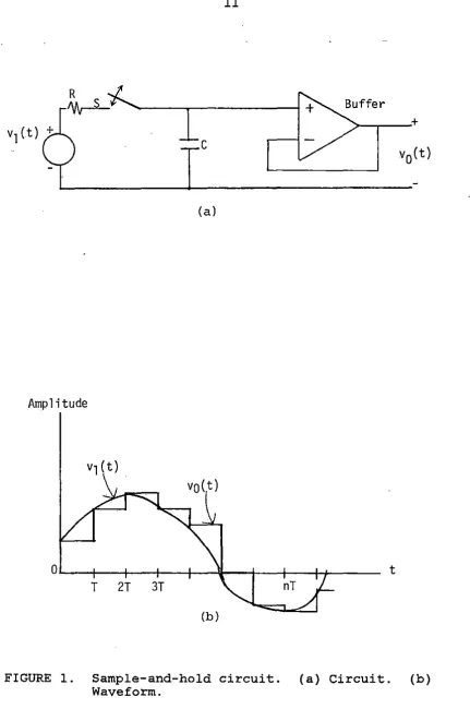
PAGE FIGURE 1. Sample-and-hold circuit. (a) Circuit. (b)
Waveform. . . 11
FIGURE 2. 2920 signal processor in a sampled data system 18 FIGURE 3.
FIGURE 4.
2920 signal processor block diagram Basic configuration of the 2920 signal processor in real-time . . . .
FIGURE 5. Five-pole, 0.7% halothane (vertical axis= .5
20
. 40
v/cm, horizontal axis= 5 msec/cm) . . . . 44 FIGURE 6. Ten-pole, 0.7% halothane (vertical axis= .5
v/cm, horizontal axis= 5 msec/cm) . . . . 45 FIGURE 7. Five-pole, 0.7% halothane (vertical axis= .5
v/cm, horizontal axis= 2 msec/cm) . . . . 46 FIGURE 8. Ten-pole, 0.7% halothane (vertical axis= .5
v/cm, horizontal axis= 2 msec/cm) . . . . 47 FIGURE 9 .. Five-pole, 1% halothane (vertical axis= .5
v/cm, horizontal axis= 2 msec/cm) . . 48
FIGURE 10. Ten-pole, 1% halbthane (vertical axis= .5
v/cm, horizontal axis= 2 msec/cm) . . 49
FIGURE 11. Five-pole, 2% halothane (vertical axis= . 5
v/cm, horizonta.l axis= 2 msec/cm) . . SO
FIGURE 12. Ten-pole, 2% halothane (vertical axis= .5
v/cm, horizontal axis= 2 msec/cm) 51
FIGURE 13. Magnitude response 53
OBJECTIVE
Th~s research was a preliminary study to develop a
microcomputer instrument to noninvasively monitor the depth of anesthesia. It was planned that a number of methods of determining the depth of anesthesia would be incorporated into the microcomputer instrument. One method, the onset latency of a visual evoked response potential, has been demonstrated by individual researchers to be a credible indice of anesthesia depth (Uhl et al., 1980). Since, a microcomputer operates only 6n digital data, the visual evoked response potential must be processed by an analog-to-digital converter. Before the analog-to-analog-to-digital conversion takes place, it is necessary the visual evoked response potential enter a low-pass filter to prevent aliasing effects that can occur during the analog-to-digital conversion process (Oppenheim and Schafer, 1975).
Therefore, the main focus of this research was to study the feasibility of using the Intel Corporation 2.920 signal processing integrated circuit to filter digitally visual evoked response potentials. The 2920 processor combines an analog-to-digital converter, an arithmetic processor, and a
'
2
LITERATURE REVIEW
Visual Evoked Response
Electrical recordings from the exposed surface of the brain or from the scalp reveal a continuous oscillating activity. A record of the electrical potentials is called an electroencephalogram (EEG). The EEG has been found
useful in areas of clinical diagnosis of brain pathology and as a measure of the level of consciousness, but is
inadequate in understanding brain function in vision (Perry and Childers, 1969). The visual evoked response (VER) is a waveform immersed in the EEG which is generated by an
external 'photic stimulation. Due to random noise and the very small magnitude of the EEG (5 to 10 microvolts), a
repetitive stimulus and the technique of signal averaging mus.t be used to separate the VER from the EEG (Perry and Childers, 1969).
The EEG is a complex representation of all electrical activity that goes on in the brain, and therefore lacks specificity. It has been found that the VER might be a better index of anesthetic effect than the EEG (Uhl et al.,
1980). Uhl et al. (1980) research data indicated that the recorded visual evoked responses during surgical anesthesia with halothane are qualitatively very similar to those
4
·1atency of the VER progressively increased with increasing alveolar anesthetic concentration. They then concluded that latency measurements of t:he VER could be used as a possible tool in monitoring anesthesia depth.
As pointed out by Ackmann et al. ( 1979), disturbances of intracranial blood flow are associated with amplitude
reductions of the evoked potential, and volume-occupy_ing lesions are associated with waveform changes. They claim that clinically, the most important features of evoked
potentials are general waveshape, latency, and amplitude of the various peaks and troughs. However, the main objective of their study was to determine a suitable upper frequency cutoff of their digital filter. They concluded that the frequency content of the records analyzed were largely contained in a band £rom from O to 200 Hz. They also felt that zero phase shift is necessary to prevent waveform distortion, namely latency and morphology of the evoked potential. Based on a frequency analysis using the Fast Fourier Transform, a ten-pole, low-pass, Butterworth filter was chosen.
out. Therefore, the interpretation of their results is based on incorrect data. Bennett et al. (1971) used a
system bandpass of 3 Hz to 1 kHz in defining a set of
statistical models that would provide information concerning the range of the normal visual evoked response parameters.
A review of a number of similar articles revealed that there is no agreed upon system bandpass range to filter evoked potentials correctly. However, there is a general concensus that the major frequencies of interest lie in the 1 to 50. Hz range. Based on this, the system bandpass in this research was chosen to be 1 to 100 Hz. The high frequency components of
a
visual evoked potential are not important in determining onset latency changes.Microprocessor-Based Digital Filter
Conventional analog filter circuits use components such as operational amplifiers, transistors, precision resistors, capacitors, and diodes. The value of these components is specified within tolerances. Therefore, replacing defective parts may change the original specification of the circuit. Also, in a production environment, no two circuits will be exactly the same. Troubleshooting an analog filter circuit can be a time consuming task, since there is more than one component making up the analog circuit.
6
a special computer on a single integrated circuit called the microprocessor. Digital filtering is a computational
process in which a sequence of input numbers are converted into a sequence of output numbers by way of addition,
multiplication by constants, and delays. A microprocessor can be p,rogrammed to perform this type of processing.
Agarwal and Priemer (1979) used the Intel 8080A
microprocessor to implement their digital filter algorithm. The signal processing system consisted of three printed circuit boards. One board was a complete microcomputer which contained the 8080A processor, memory, and the necessary interface circuitry. The other two boards contained the data acquisition system and a hardware multiplier.
Although the 8080A has the necessary instructions to perform the required multiplications, the researchers decided to implement the multiplication process with a single integrated circuit multiplier in order to speed up processing. The effective on-line data processing rate was
2 kHz per s-order section (sis complex parameter). For a two-pole network, the sampling rate is 1 kHz, and for a four-pole network, the sampling rate is 500 Hz.
Walstrom (1979) also used the Intel 8080A
designed to sample an electrocardiograph signal. The hardware consisted of a microprocessor with the, necessary interface circuity, the data acquisition components, arid a hardware multiplier. A sampling rate of 360 Hz was used. The author concluded that the 8080A digital bandpass filter
system was a workable system, bµt lacked many refinements which would enhance the overall operation. An improvement
suggested by the author was to implement the filter on the new generation of 16-bit microprocessors such as the Intel 8086, the Zilog Z-8000, or the Motorola 68000. These
microprocessors offer greater program efficiency, faster instruction cycle time, and true 16-bit operations versus the pseudo 16-bit operations performed by the Intel 8080A and the Motorola 6809 ..
Typical microprocessors in use today are the Motorola 6800/6809 or the Intel 8080/8085. These microprocessors, as well as most digital microprocessors, are designed for
general data processing and not for high-speed complex signal analysis. A microprocessor-based digital signal processing system can operate as a signal processor at
frequencies to only a few hundred hertz.
In contrast, most general signal processing frequencies are in the kilohertz range. Signals such as speech,
electrocardiogram, electroretinogram, and
8
cases, multiple signals must be processed in parallel.
Therefore, due to the high sampling rates and the complexity of the signal,
a
general purpose microprocessor is not well suited for signal processing applications. A totallyBACKGROUND
Digital Filters
A digital filter implemented in software processes a sequence of input numbers to produce a predefined sequence of output numbers. The central element in the concept of the digital filter is the linear difference equation as defined by Oppenheim and Schafer (1975).
y(n) + b1y(n-1) + b2y(n-2) + .•. + bky(n-k)
=
a0x(n) + a1x(n-1) + a2x(n-2) + ... + akx(n-k)
where,
x(n)
=
input sequence I samplesy(n)
=
output sequence samplesak and bk
=
filter weightsk = order of the difference equation
One way of deriving the linear difference equation is to start with classical analog-filter theory. Once a set of frequency characteristics has been defined, the classical theory is used to derive the analog transfer function. Corresponding to this transfer function is a differential equation. From the definition of the derivative, as the independent variable (sampling period in this case)
approaches zero, the differential equation can be
10
variable. Therefore, as the sampling interval approaches zero, the approximation improves. This procedure of
deriving a linear difference equation from a differential equation is simple. However, an alternative procedure proves to be more advantageous. This procedure is called the z-transform.
The first step in developing the z-transform is to note that signal samples of zero duration do not exist in any physical system. Any sampling operation implemented in hardware is necessarily associated with a holding operation producing discrete samples of nonzero duration.
Consequently, a sample-and-hold operation will transform a continuous time signal into a stair-step output signal. As the sampling frequency increases, the stair-step will
approach zero; hence, the sampled waveform will look more like a continuous signal in time.
Th~ most widely used sample-and-hold circuit has the
form shown in Figure l(a). When the input signal is
continuous in time, the circuit produces a stair-step output waveform as shown in Figure l(b).
A great deal of valuable information about the sampling process and the stair-step output waveform can be obtained from the Laplace transform of the stair-step signal. This transform is
m
c
(al
Amplitude
t
T 2T 3T
nT
(b)
[image:16.568.54.486.56.718.2]12
where,
V0(s) =sampled Laplace signal v0(t) =sampled signal in time
By taking the Laplace transform of the stair-step signal, and from the definition of the integral, the integral can be expressed as the sum of infinitely many integrals, each spanning the time interval of one step in the waveform (Oppenheim and Schafer, 1975). The evaluation of these integrals yields:
1 - exp(-sT) ao
V
0(s)= --- In=O v1 (nT)exp(-nsT).s
Implicit in this equation is the fact that during each step in the waveform, v0 (t) is constant and equal to the value of
v1 (t) at the beginning of the step.
The factor preceding the summation is the result of the nonzero duration of the sample-and-hold operation.
Oppenheim and Schafer (1975) has shown that this factor is the (sin x)/x function that amplitude modulates the
magnitude of the filter function. The (sin x)/x often appears in the literature as
sin( 11*w/w0 )
w = radian frequency
w0 = radian sampling frequency
The sampling theorem indicates that the sampling rate
must be greater than twice the highest frequency component of the input signal. If this condition is satisfied, the samples will contain all the significant information of the
original signal. Therefore, if the sampling frequency is much greater than the highest frequency component, the (sin
x)/x function will approach one, and consequently, amplitude distortion will be negligible.
The summation contains the values of all the samples of the input signal v1 (t), and it also contains the instant of time t=nT at which each sample occurs. Thus, it contains
complete information about the sequence of samples v1 (nT).
It is, therefore, common practice to associate the summation with the process of sampling the input signal.
By defining a new symbol
z= exp( sT),
the z-transform of the sequence of sample values becomes
V1(z)= l:n=O v"' 1 (nT)z . -n
14
input signal. Therefore, the z-n symbol represents a time delay, where n is the nth delay.
The important point is, given an arbitrary sequence of uniformly spaced sample values, the z-transform of the
sequence can be written by inspection. Then, the Laplace transform of the associated stair-step wave can be written, and from the Laplace transform the frequency spectrum of the
waveform· can be calculated.
The z-transform, as developed, is a special form of the Laplace transform with a new variable, z= exp(sT). Also, it has been shown that the (sin x)/x weighting function is
introduced when nonzero duration sampling occurs.
It will now be shown how an analog transfer function in the s-domain is transformed into a transfer function in the z-domain, and finally, how the linear difference equation is derived from the z-transfer function.
The appropriate transform for a difference equation is the z-transform, which performs the same role with
difference equations as the Laplace transform carries out for differential equations. The use of the z-transform permits the specification of a digital filter from the s-transfer function directly in terms of delays,
multiplications, and additions which is the correct form for hardware or software implementation.
filters may be realized. The Finite Impulse Response (FIR), or non-recursive filter, represents the summation of a
limited number of input terms and thus has a finite memory. It has excellent phase characteristics but requires a large number of terms to obtain a relatively sharp attenuation characteristic. The Infinite Impulse Response (!IR) filter represents the summation of both input and output terms so that it can be considered as having an infinite memory. The !IR filter requires relatively few terms for similar
attenuation characteristics, but possesses relatively poor phase response. Since phase response is not important and memory storage is limited in this application, the !IR filter will be developed.
The difference equation for an !IR filter is
y(n)=
Taking the z-transform of the difference equation yields:
H(z)=
1
-Stanley (1975) suggests that since the design of an !IR filter is stable and causal, it is convenient to assume the coefficient a0
=
1. The coefficients in the above equation16
by inspection of H(z), the difference equation for y(n) can be directly derived, hence, the digital filter is ready to be programmed into the computer. The question now becomes, how does one derive the z-transfer function H(z) from the given analog s-transfer function H(s)?
The bilinear transform is a method of transforming a function in the s-domain to a function in the z-domain. The standard form given by Stanley (1975) is
2(z-l)
s=
---T(z+l) where
T
=
sampling period in seconds.However, the bilinear transformation causes shifting of frequencies between the analog and digital transfer
functions. A correction factor suggested by Stanley (1975) is
(z-1)
s=---(z+l) and
where
w1
=
analog frequency in ra~ians/secw2
=
digital frequency in radians/sec2920 Signal Processor
With the great advances in Very Large Scale Integrated circuit technology (VLSI), it is now possible to integrate al1 the necessary real-time analog processing functio~s onto a single integrated circuit (2920 integrated package size is approximately 3.5 cm by 1.5 cm). VLSI advantages include small.size, high reliability, relatively low cost, and low-power consumption. Basically, signal processing includes the generation, filtering, detection, and modulation of signals. Algorithms for signal processing repeatedly use multiplications and additions.
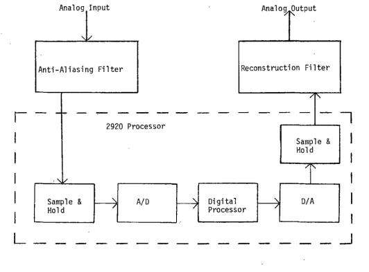
The Intel Corporation 2920 signal processor has been designed· specifically to replace analog systems in real-time applications. An overview of a sampled-data system that uses the 2920 signal processor is shown in Figure 2. First, the analog input signal encounters an anti-aliasing filter and is sampled by a sample-and-hold circuit. Next, the just acquired analog sample is then converted to a digital signal and sent to the digital processor, where a signal analysis algorithm is performed. The result from the algorithm moves to a digital-to-analog converter, where it is converted back to an analog signal. The signal sample then moves to
r
L
Analog Input
Analog Output
7 I''
I/Anti-Aliasing Filter
Reconstruction Filter
,r
'
-
- -
-
-
- - -
-
-
- - -
-
-2920 Processor
Sample
&Hold
,r
1'-' ' ,
Sample
&'
A/D
' Digital
'
D/A
Hold
I IProcessor
,
FIGURE 2. 2920 signal processor in a sampled data system
I
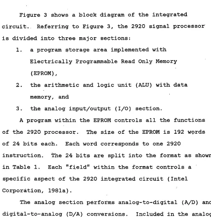
[image:23.786.122.654.49.441.2]Figure 3 shows a block diagram of the integrated
circuit.. Referring to Figure 3, the 2920 signal processor· is divided into three major sections:
1. a program storage area implemented with Electrically Programmable Read Only Memory
(EPROM),
2. the aritfunetic and logic unit (ALU} with data memory, and
3. the analog input/output (I/OJ section.
A program within the EPROM controls all the functions of the 2920 processor. The size of the EPROM is 192 W()rds of 24 bits each. Each word corresponds to one 2920
instruction. The 24 bits are split into the format as shown in Table 1. Each "field" within the format controls a
specific aspect of the 2920 integrated circuit (Intel Corporation, 198la).
The analog section performs analog-to-digital (A/DJ and digital-to-analog (D/A) conversions. Included in the analog section are the following:
1. an input multiplexer (4 inputs: SIGINO ... SIGIN3},
2. an input sample-and-hold circuit, 3. a digital-to-analog converter (D/AJ, 4. a comparator, and
[image:24.565.53.488.61.513.2]20
PROGRAM .STORAGE
(EPROM)
192 x 24
~.-r--~-~~~-r.-~=--"-;..1---.r--~-.-r-'
SI GINO
SIGINl
SIGIN2
SIGIN3
S&H
MUX
&=
CLOCK
&PROGRAM
CCLK
<----tCOUNTER
DMUX
&
S&H's
D/A
1---71--,-t--1--VREF
+5v
-5v GND
FIGURE 3. 2920 signal processor block diagram
[image:25.568.62.496.142.630.2]TABLE 1
.
2920 instruction formatALU B A Shift Analog
·. Instruction Address Address Code Instructi.on
. (3 bits) (6 l:>its) (6 bits) (4 bits) (5 bits)
A special register called the DAR (digital/analog register) acts as an interface between the digital and
analog sections. It is 9 bits wide (one sign bit and eight amplitude bits), occupying the nine most significant
positions of a word whose other bits are set to ones (Intel Corporation, 198la). The DAR output is also tied directly to the D/A inputs. The DAR is used as a successive
approximation register for analog-to-digital conversion, under control of the analog function instruction field.
In some applications., the output signal need only be a logic level of one or zero. SIGOUT pins can be selected to be either analog output or digital output (Intel
Corporation, l98la). The analog mode allows the full 9-bit D/A output to be present. The digital mode requires a LIM
instruction to yield a zero or one decision (Intel Corporation, 1979).
22
using 25-bit two's complement arithmetic. The normal range of any variable "x" is considered to be
-1< x <l
and the smallest resolvable change "y", in any variable is given by (Intel Corporation, 198la),
y= 2-24= 5.96x10⁻⁹ •
A positive voltage reference supply (VREF) of one volt is provided to the D/A converter to establish its voltage range. If digital output is required, VREF > 1.5 volts is necessary (Intel Corporation, 198la).
The EPROM word addresses are numbered from 0 to 191 (decimal notation). During normal operation, the program counter begins at word address zero and the program
sequentially executes through word address 191, or when an End of Program (EOP) instruction is encountered (Intel Corporation, 1979).· The cycle then begins again at word
address zero.
Program length determines the sampling frequency of the analog S·ignal. If an input is sampled once per program
pass, the sampling frequency is
l/(NT) where
T
=
2920 instruction cycle time.Example: if N =. 192 and T = 800 nanoseconds, then the sampling rate is approximately 6510 Hz.
The EPROM fetch/execute cycle is "pipelined" four deep, meaning "the next four instructions are being fetched while the previously fetched instructions are being executed. The term "pipeline" refers to the fact that the processor has several hardware components which perform different
operations simultaneously and pass data from one component to the next as through a pipe.
Limitations of the·2920 Signal Processor
The 2920 signal processor limitations are established by the size of the memory, the speed and capability of the processor, and the resolution of the A/D and D/A converters. Currently, ther.e are three different 2920 signal processors being produced by the Intel Corporation. They are the 400 ns, 600 ns and 800 ns processors (Intel Corporation, 198la). The different processor speeds refer to one instruction cycle time. For full 192 instructions, the sampling rates are approximately 13020 Hz, 8680 Hz, and 6510 Hz
respectively. Faster sampling rates are achieved with smaller size programs.
24
of the RAM limits the number of poles to less than 40, or less than 20 complex conjugate pairs. The number of EPROM words needed to realize a complex conjugate pole pair is
approximately 10 to 11 (Intel Corporation, 1980a).
When an analog signal is digitized, it is "quantized." Theoretically, an infinite number of bits are required to represent each analog sample exactly (Oppenheim and Schafer, 1975). Of course, physical limitations preclude sampling with infinite precision. Therefore, each sample must be either truncated or rounded to fit a finite-length register.
Oppenheim and Schafer (1975) point out that the signal-tonois.e ratio (SNR) in decibels (dB) can be approximated by the following equation:
SNR = 6N where
N =number of bits in the A/D register (DAR).
The 2920 signal processor has a programmable A/D
DESIGN PROCESS
Filter Specification
Since the major frequencies of interest in an evoked potential lie in the 1 to 50 Hz range, a 0 to 100 Hz
passband was chosen. The required Nyquist sampling
frequency must then be greater than 200 Hz. The derived filter programs required less than the maximum 192
instructions,. but the EPROM was programmed for the full 192 instructions to give a sampling rate of 6510 Hz. This was done for the sake of convenience.
The type of filter chosen was a Butterworth filter, which is char;;i.cterized by a maximally flat passband (Budak, 1974). A Chebyshev, Elliptic, or Bessel filter would have worked just as well if their passbands were optimized.
Fifth-Order Filter Design
For a 3 dB passband, the squared magnitude function for a Butterworth filter is given by Budak (1974) as
where
n = order
1
IG(s)l 2= H(s)=
---1 + (W/W3)2n
26
As described by Budak (1974), a fifth-order, 3 dB
passband, 1 rad/s cutoff transfer function in cascaded form is
where
1
(s +
1)
1
H
2 (s)=
---s2 + 0.618s + 1
1
H
3 (s)=
---s2 + 1. 618s + 1
The cascaded form is a series representation where the output of an individual section becomes the input to the next section. The significance of the preceding result is all of the decomposition can take place on the analog
function, for which tabulated information is given by Stanley (1975), and for which the manipulative steps of decomposition are usually easier.
H{s)=
The bilinear transformation is then applied to the
individual section and the discrete transfer function of the digital filter will be of the form (Oppenheim and Schafer,
1975)
H(z)= 1
-The H(z) transfer function is a bilinear transformation of H(s) with the correction factor taken into account. All the coefficients in H{z) were calculated by the formulas given by Stanley (1975). Consequently, a fifth-order Butterworth z-transform filter is
where
H1
(z)
=
---H2(Z)
=
---~---28
where
ai1
=
0.9079 bia = 4.6068xlo- 2 baa=
2.1585xlo-aa21 = 1. 9331 bi1 = bi a ba1 = 2bao
a22 =-0.9422 b2o = 2 . .2S94x10-a ba2
=
baaaa1
=
1.8467 b21 = 2b2aaa2 =-0.8554 b22 = b2a
Then, by inspection the difference equations can be determined for each function. The output of section one will become the input to section two and the output of
section two will become the input to section three. First Section
where
X2 (n) - Y1 (n) Second Section
where
Y2(n)= az1Y2(n-l). + az2Y2(n-2) + b 2 aX2(n) + bz1X2(n-l) + b 22X2(n-2)
Third Section
where
Ya(n)= aa1Ya(n-l) + aa 2Ya(n-2),+ ba~x~(n)
+ ba 1xa(n-1) + ba 2xa(n-2)
Tenth-Order Filter Design
The derivation of the tenth-order digital filter follows the same procedure as the fifth-order filter. As given by Budak (1974), a tenth-order 3 dB passband, 1 rad/s cutoff transfer function in a cascade form is
where
1
H1(s)
=
---s2 + 0.3128s + 1
1
H2(s)
=
---s2 + 0.9080s + 1
1
H3 (s)
=
s2 + 1.4142s + 1
1
H4(s)
=
---s2 + l.7820s + 11
H
5(s)=
s2 + 1.9754s + 1
The tenth-order Butterworth z-transform filter is
30
and
n = 1,2,3,4,5 and
a11 = 1.9611 b10 = 2 .2922x10- 3 bs o = 2.1245x10- 3
a12 =-0. 9703. b11 = 2b1 0 bs 1 = 2bs o
a21 = 1.9073 b12 = b1 0 b52 = bs o
a22 =-0.9162 b20 = 2.2292x10- 3
aa1 = 1.8637 ·b21 = 2b20
aa2 =-0.8724 b22 = b20
a41 = l.8333 b3 0 = 2.1783x10- 3
a42 =-0.8419 b3.1 = 2bao
as 1 = l.8177 b32 = bao
as2 =-0.8262 b40 = 2.1428x10- 3
b41 = 2b40 b42 = b40 The difference equations are:
First Section
Y1(n)= a11Y1(n-l) + a12Y1(n-2) + b 1 ox1 (n)
+ b11X1(n-l) + b 12x 1 (n-2)
where
x2 (n) = y1 (n)
Second S.ection
Y2(n)= a21Y2(n-l) + a 22Y2 (n-2) + b 20 x 2 (n)
where
Third Section
where
y 3(n)= a 31 y 3 (n-l) + a32Y3(n-2) + b3aX3(n)
+ b 31 x 3 (n-l) + b32X3(n-2)
x4 (n)
=
y3(n)Fourth Section
where
y4(n)= a41y 4 (n-l) + a42Y4(n-2) + b4aX4(n)
+ b 41 x 4 (n-l) + b42X4(n-2)
Xs (n) = y4.(n) Fifth Section
where
y5(n)= a 51 y5(n-l) + aszYs(n-2) + bsaXs(n)
+ bs 1x5(n-l) + bszXs(n-2)
y5(n) =Filtered sample
Software Development Tools
To program the 2920 signal processor for a specific function, the 2920 software support package (Intel
Corporation, 1979, Intel Corporation, 1980a, Intel
32
including testing and debugging, before the 2920 signal
processo~ is used in the actual application.
2920 Assembler
The 2920 Assembler (Intel Corporation, 1979) translates symbolic assembly language programs into machine-readable code. The assembler generates a listing file and an object code file (in hexadecimal). A listing file lists the source code with the corresponding machine code and memory
locations. It also includes comments and titles (if any), error and warning diagnostics, the number of RAM and ROM locations used, and a table of user-defined symbols. A listing of the fifth-order Butterworth filter is shown in Appendix A and the tenth-order is shown in Appendix B. The object code files, also included, contain machine-readable code used to program the 2920 processor for real-time
testing or for the use with the 2920 Simulator (Intel Corporation, l980b), for off-line debugging.
2920 Software/Compiler
The SPAS20 Signal Processing Applications
Software/Compiler accepts high-level (English-like) language inptit and produces 2920 assembly language code (Intel
Corporation, l980a). The SPAS20 Compiler gives the designer substantial interactive manipulation of parameters and
optimization of code size and error limits.
Two.main functions of the SPAS20 Compiler are: 1. to make it easy to specify, alter, and review
design parameters, and
2. to save time in writing the detailed steps
required to implement the necessary functions in assembly language code.
A macro is a labeled block of commands, executed in sequence when the macro name is used as a command. The block of commands is also referred to as the macro body. The SPAS20 Compiler provides a number of macros, which include the Butterworth filter and the bilinear transform. Parameters specified when invoking the Butterworth macro are:
1. order of the filter,
.2. 3 dB cutoff frequency in hertz, and 3. a label to uniquely identify a pole.
The output of the Butterworth macro is the poles specified in the s-domain.
34
section cascaded with the other filter sections to produce the required digital filter.
The command CODE is used to produce the required 2920 instructions for each pole section. An error parameter is imposed on the CODE command to minimize movement of the pole from the original coordinates. This constraint was equal to ±Q .. QOOl. Based on this constraint, the SPAS20 Compiler
derives the necessary instructions to minimize the specified movement. This position error parameter is needed because the assembly language program generated by the CODE command implements a filter stage corresponding to a pole that has a slightly different location than the specified original pole. ·This difference is due to a finite word length (25 bits). After the compilation has been performed, the pole is moved to the location matching the code generated.
Once all the poles have been coded, the design is now ready to be assembled by the 2920 Assembler (Intel
Corporation, 1979). Appendix C shows an example of the use of the SPAS20 Compiler in generating a fifth-order
Butterworth filter. For additional details, refer to Intel Corporation (l980a).
2920 Simulator
The 2920 Simulator simulates the program as it would be executed in the 2920 integrated circuit. The simulator
clock, memory locations and other points of interest in the signal processor when the performance and problems of the program are analyzed. Although the simulator simulates the functions of the 2920 signal processor, the simulator
executes much more slowly than the 2920 processor. The 2920 processor is a real-time signal processor, but the simulator is a logical time signal processor.
Since a digital filter algorithm involves arithmetic operations, proper scaling must be implemented to prevent overflow. Three pins on the 2920 processor can be used for hardware debugging:
1. end of program (EOP), 2_. overflow (OF), and
3. the instruction cycle (CCLK).
With the aid of the simulator, the designer can determine the instruction at which a register overflows.
Appendix
D
presents a demonstration of the 2920Simulator. Initially, the designer directs the simulator to load the program to be simulated from disk to RAM. The next command, TPROG sets the sample period. In this case, the sample period is 153.6 microseconds (192 instructions multiplied by 800 nanoseconds instruction cycle time).
2. HPI = PI/2 3. TPI = 2*PI 4. ONE = l. 00.
The input function specified in Appendix D is
IND= sin(lOO*TPI*TIME)
which indicates a sine wave at 100 Hz.
The command CONSOLE OFF directs the simulator not to output the TRACE data to the console during simulation. This command increases the speed of the simulation process, but doesn't affect the results of the simulation. To
initiate the simulation of the program, the SIMULATE FROM 0 (zero) command is given. With a sine wave input of 100 Hz, the simulation time is approximately one second per pass of the simulated program. Therefore, there is a maximum of 100
sec.ends before the SIMULATION TERMINATED response is printed on the console. The end of simulation will occur according
'
to what was specified in the BREAKPOINT command. The break in simulation is to occur if OVF=l or if 100 passes through the simulated program has been complet~d.
When the OVF command is entered and the flag is
observed to be equal to zero (OVF=O, overflow flag= zero), the break then occurs on the lOOth pass through the
38
(OVF=l), then by entering in the PC command, the simulator will print out the word address of the overflow.
The PRINT ALL command displays the entire TRACE buffer. When the GRAPHICS ON command i.s specified, each trace i tern's changing value is displayed as a curve. Since TIME was the first TRACE item specified, the vertical axis is labeled in seconds,. For the horizontal axis, the left most value is minus one and the right most value is plus one. This range corresponds to the output limits of the 2920 processor. The graph of ones' and twos' corresponds to the data values of !NO and OUTO respectively.
The following commands are a summary of what has just been described to simulate a five-pole, 100 Hz cutoff, Butterworth filter:
1. LOAD SPROG.HEX
2. TPROG=l92*0.0000008 3. TRACE=TIME,INO,OUTO 4. QUALIFIER=PC=O
5. SIZE=l92
6. BREAKPOINT=OVF=l OR PC=O AND TIME<!:lOO*TPROG 7. INO=SIN(lOO*TPI*TIME)
8. CONSOLE OFF 9. SIMULATE FROM 0 10. OVF
12. GRAPHICS ON 13. PRINT ALL
Once simulation is completed and the designer is satisfied with the performance of the program, the next step is to
install the program into the EPROM of the 2920 integrated circuit. The 2920 integrated circuit is inserted into the socket of the Intel Universal Prom Programmer (UPP) (Intel Corporation, 198lc). The software package used to install the program into the EPROM of the 2920 signal processor is called the UPM which runs under ISIS-II. Instructions on the use of the UPM are given by Intel Corporation (198lc).
The fully programmed 2920 signal processor is then inserted into the Intel SDK-2920 kit (Intel Corporation, 198ld, Intel Corporation, 198le), which has the necessary interface circuitry. Figure 4 represents the basic
configuration of the 2920 signal processor for real-time applications. Intel Corporation (198la) suggested using a value of 1000 pf for the input sampling capacitor to yield an offset of less than minus one-half of the least
Analog Input
Anti-Aliasing
Filter
Sample
&Hold
Capacitor
f
40
2920
Processor
+5v
0
Analog Output
Reconstruction
Filter
CJ
5 MHzJ
10 pf-5v
[image:45.563.86.427.153.570.2]COLLECTION OF EVOKED POTENTIALS
A dog anesthetized with halothane was outfitted with scalp electrodes. Cortical electrical activity was
amplified with a Grass amplifier (model P511) having a
bandpass of 1 to 100 Hz. Gain was set at 1000 and the 60 Hz notch filter was enabled on the Grass amplifier. Averaged visual evoked responses were obtained following 32
presentations of a visual stimulus using an averaging
computer (Nicole~model 1072). A strobe light placed 10 cm away, on axis, from the dog's right cornea was illuminated every 500 milliseconds to serve as the visual stimulus. The averaging computer was synchronized to begin sampling at the flash onset and the averaging period had a duration of 256 milliseconds following the flash onset. During the
averaging period, 1023 samples were collected in which the time interval between each sample was 250 microseconds.
Recordings of the averaged visual evoked responses were then made on a Honeywell 5600 tape recorder.
End-tidal halothane concentrations were measured with a calibrated Beckman LB-2 gas analyzer. The recorded visual evoked responses were performed at 0.7, 1.0, and 2.0 per cent end-tidal halothane concentrations. The visual evoked response recordings were initiated 15 minutes after
42
minutes.
RESULTS
The following oscilloscope recordings represent the • averaged visual evoked responses at three different
concentrations of halothane. The top trace in each
recording is the unfiltered waveform and the bottom trace is the filtered response.
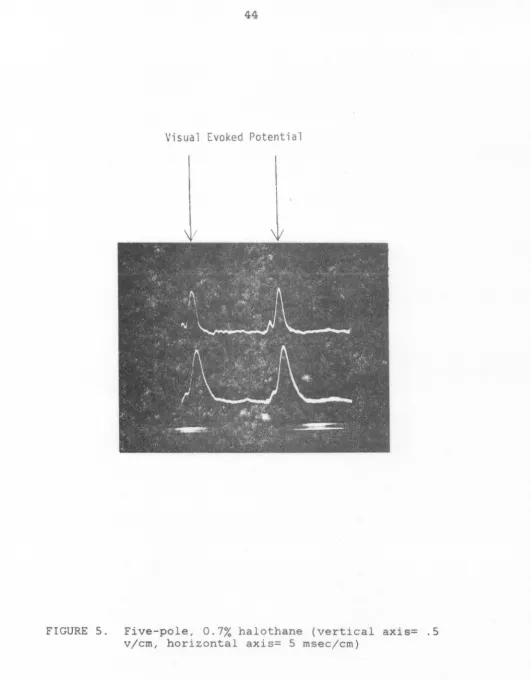
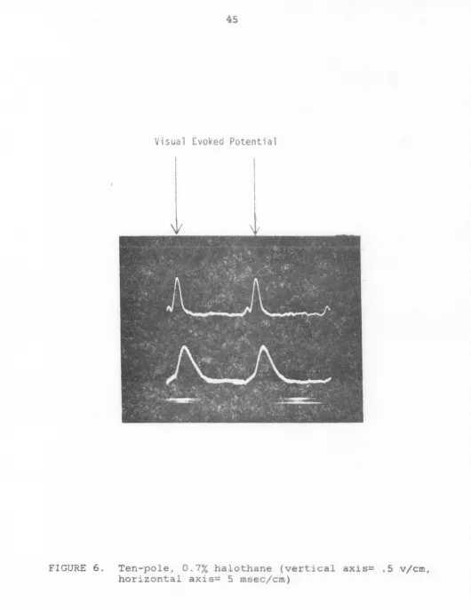
Figure 5 represents the five-pole Butterworth filter at a 0.7% concentration of halothane. Figure 6 represents the
ten~pole Butterworth filter at a 0.7% concentration of
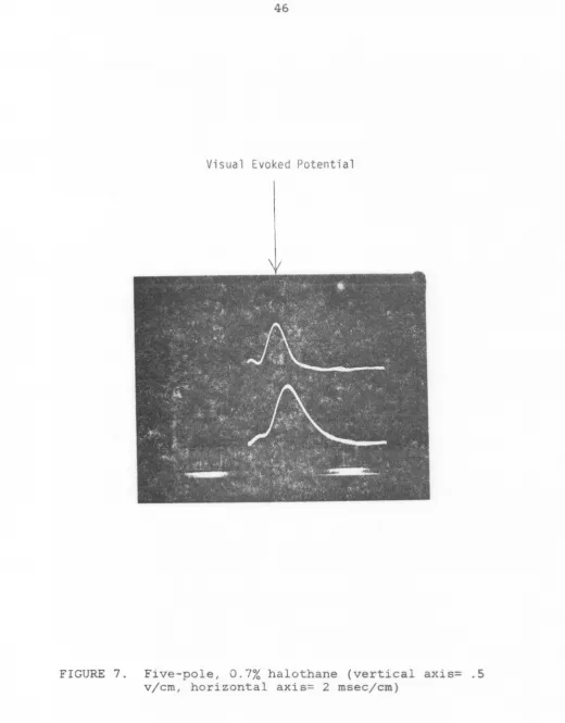
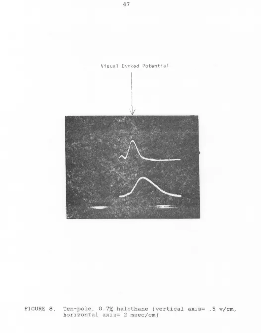
halothane. Figures 7 and 8 are recorded at a faster
oscilloscope sweep speed to enhance the definition of the waveform.
Figure 9 represents the five-pole filter at a 1% concentration of halothane. Figure 10 represents the ten-pole filter at a 1% concentration of halothane. The
multiple images of the waveform are due to the incorrect triggering of the oscilloscope which was beyond the author's control. Note how the ten-pole filter severely diminishes the amplitude of the evoked potential.
Figure 11 represents the five-pole filter at a 2% concentration of halothane. Figure 12 represents the ten-pole filter at a 2% concentration of halothane. Notice
44
Visual Evoked Potential
[image:49.557.10.541.38.719.2]Visual Evoked Potential
[image:50.559.11.541.34.721.2]46
Visual Evoked Potential
[image:51.543.8.529.47.713.2]Visual Evo ked Potential
I
I
t
[image:52.549.10.536.44.715.2]48
Visual Evoked Potential
[image:53.558.11.534.41.721.2]Visual Evoked Potential
1
[image:54.566.9.548.42.719.2]50
Visual Evoked Potential
[image:55.560.10.535.34.716.2]Visual Evoked Potential
[image:56.559.16.549.37.713.2]52
The ten-pole filter responses display slow rise times and longer settling times in comparison to the five-pole filter responses. This is characteristic of a higher order Butterworth filter (Johnson, 1976). In comparison, a Bessel
filter will have a shorter rise time as the order of the filter increases (Johnson, 1976).
Since, the raw visual evoked potentials· were already frequency band-limited at 100 Hz before being processed by the 2920 signal processor, it was necessary to perform
frequency and phase studies of the 2920 signal processor. A ±1 volt sine wave generated from an Interstate Electronics Corporation Model F34 Function Generator was fed into the input
of
the 2920 signal processor. The output signalversus the input signal in terms of normalized magnitude and phase responses, are depicted in Figure 13 and Figure 14 respectively. The magnitude is reasonably flat and has a fairly linear phase response in the passband for both the five pole and ten pole filters.
A Tektronix Model 465 Oscilloscope was used to monitor the input and output ports of the 2920 signal processor. Consequently, the magnitude and phase data were calculated from the waveforms displayed on the cathode ray tube.
·'
1.0
0.9
0.
Q) '
-0
0. 7
:J
+-' ·~
~
01
"' 0.6
::;:-0
Q)
N ·~
0.5
~
"'
E
'-0
z
0.4
0.3
0.2
0. l
0
n=lO
0.2 0.4 0.6 0.8 1.0 1.2 1.4 1.6 1.8 2.0
W/w
3n = order of the Butterworth filter
w3 = cutoff radian frequency
[image:58.565.84.484.72.598.2]!
Vl
QJ
0
-100
~200
-300
~ -400
0>
QJ
Cl
-500
-600
-700.
54
w/w3
0.2 0.4 0.6 0.8 1.0 1.2 l.4 1.6 1.8 2.0
n
=
order of the Butterworth filter
w3
=cutoff radian frequency
[image:59.566.58.491.44.676.2]::-CONCLUSIONS
The visual evoked potentials at a 0.7% halothane concentration show the fi 1 tering and analog-to-di.gi tal
actions of the 2920 signal processor. However, pictorially, the visual evoked potentials at 1% and 2% halothane
concentrations portray multiple images due to incorrect triggering of the oscilloscope. From a morphological point of view, the 2920 signal processor performs correctly in filtering the visual evoked potentials at a 0.7% halothane concentration. It clearly shows the slow rise times and longer settling times that are associated with higher order Butterworth filters.
The ten-pole filter severely diminished the amplitude of the visual evoked potentials at 1% and 2% con.centrations of halothane. The magnitude response portrayed in Figure 13 show the amplitude response should be at least 80% of the original signal.
The amplitude responses of the five-pole filter at 1% and 2% halothane concentrations were diminished but not as severe as the responses from the ten-pole filter. However, the magnitude response given in Figure 13 for the five-pole filter show the magnitude should be at least 80% of the original signal. Again, as in the case of the ten-pole
56
concentration does the 2920 signal processor support the results of the magnitude responses shown in Figure 13.
The magnitude and phase responses depicted in Figure 13 and Figure 14 respectively, clearly show the 2920 signal processor to perform as a Butterworth low-pass filter should
(Budak, .. 1974). On the other hand, the results of the
filtering action of the evoked potentials at the 1% and 2% halothane concentrations prove somewhat contradictory.
Given the above mentioned results, the author cannot offer any absolute answers to the perplexity of the
findings. More experiments will have to be performed and the results scrutinized to determine if the 2920 signal proces.sor is suitable as a low-pass filter and analog-to-digital converter preprocessor for the microcomputer instrument.
In :regards to the 2920 software support package, it is a very powerful tool in developing visual evoked potential filter programs for the 2920 signal processor. The SPAS20 Compiler program provides the necessary commands to specify and develop the low-pass Butterworth filter easily. The 2920 Simulator allows the designer to thoroughly test the program before programming the 2920 signal processor. Also, the simulator has the capability to graph the input and output waveforms versus time on a hard copy device.
BIBLIOGRAPHY
Ackmann, J. J., P. P. Elko, and S .. J. Wu. 1979. Digital filtering of on-line evoked potentials. International Journal of Bio-Medical Computing 10:291-303.
Agarwal, P., R. Priemer. 1979. Microprocessor based digital signal processing system. Comput. Biol. Med. 9:87-95.
Bennett, J. R., J. S. Macdonald, S. M. Drance, and K. Uenoyama·. 1971. Some statistical properties of the visual evoked potential in man and their application as a criterion of normality. I.E.E.E. Transactions on Bio-Medical Engineering BME-18(1):23-34.
Budak, A. 1974. Passiye and active network analysis and synthesis. Houghton Mifflin Company, Boston, MA.
Desmedt, J. E., E. Brunko, J. Debecker, and J. Carmeliet. 1974.· The system bandpass required to avoid distortion of early components when averaging somatosensory evoked potentials. Electroencephalography and Clinical
Neurophysiology 37:407-410.
Intel Corporation. 1975. Intellec 800 microcomputer development system operator's manual. Number 9800129A. Santa Clara, California.
Intel Corporation. 1979. 2920 assembly language manual. Number 9800987-01. Santa Clara, California.
Intel Corporation. 1980a. 2920 signal processing· applications software/compiler user's gu-ide. Number 121529-002, Revision B. Santa Clara, California. Intel Corporation. 1980b. 2920 simulator user's guide.
Number 9800988-02, Revision B. Santa Clara, California. Intel Corporation. 198la. Component data catalog. Pages
4-45 to 4-55. Santa Clara, California.
Intel Corporation. 198lb. ISIS-II user's guide. Number 9800306-06. Santa Clara, California.
58
Intel Corporation. assembly manual. California.
198ld, SDK-2920 system design kit Number 162421-002. Santa Clara,
Intel Corporation. 198le. SDK-2920 system design kit user's guide. Number 162418-001, Revision A. Santa Clara, California.
Johnson, D. E. 1976. Introduction to filter theory. Prentice~Hall, Inc., Englewood Cliffs, New Jersey.
Oppenheim, A. analysis. Jersey.
V. and R. W. Schafer. 1975. Digital signal Prentice-Hall, Inc., Englewood Cliffs, New
Perry, N. W. and D. G. Childers.. 1969. evoked response: method and theory. Publisher, Springfield, Illinois.
The human visual Charles C. Thomas,
Stanley, W. D. 1975. Digital signal processing. Reston Publishing Company, Inc., Reston, Virginia.
Uhl, R. R., K. C. Squires, D. L. Bruce, and A. Starr. 1980. Effect of halothane anesthesia on the human cortical visual evoked response. Anesthesiology 53:273-276. Walstrom, R. W. 1979. A microproc<;!ssor controlled digital
APPENDIX A: FIFTH-ORDER BUTTERWORTH FILTER LISTING
ISIS-II 2920 ASSEMBLER v1.o
ASSEMBLER INVOKEU
BY:
:F1:AS2920 5PROG.BUTLINE LDC OB,JECT SOURCE STATEMENT 1
2 ;A/D CONVERSION ROUTINE
3 ;
4 0 40C6EF LIIA DAR,KPO ;CLEAR DAR
5 1 OOOOEF INO
6 2 OOOOEF INO
7 3 OOOOEF INO
8 4 OOOOEF INO
9 5 OOOOEF INO
10 6 OOOOEF INO
11 7 OOOOEF INO
12 8 OOOOEF INO
13 9 4000EF NOP
14 10 6000EF CVTS
15 11 4000EF NOP
16 12 4000EF NOP
17 13 7100EF CVT7
18 14 4000EF NOP
19 15 4000EF NOP
20 16 6100EF CVT6
21 17 4000EF NOP
22 18 4000EF NOF·
23 19 5100EF CVT5
24 20 4000EF NOP
25 21 4000EF NOP
26 22 4100EF CVT4
27 23 4000EF NOP
28 24 4000EF NOF·
29 25 3100EF CVT3
30 26 4000EF NOP
31 27 4000EF NOP
32 28 2100EF CVT2
33 29 4000EF NOP
34 30 4000EF NOP
35 31 1100EF CVT1
36 32 4000EF NOP
37 33 4000EF NOP
38 34 0100EF CVTO
39 35 4000EF NOP
40
42 43 44 45 46 47 48 49 50 51 52
36 40222E
60
;5TH ORDER BUTTERWORTH FILTER ;ioo
HZ
CUTOFF;
;
;
LDA INO_PlOrDAR,R2
OUT2_P10 EQU TEMP
37 4200FF LDA OUT2_P10.0UTl_P10.ROO
; OUT2-P10=1.00000000*0UT1_P10 ~8 460BEF LDA ouT1_p10.ouTo_P10.Roo
; OUT1_P10=1,00000000*0UTO_~l0
53 39 44087E LDA OUTO_p10.ouT2_P10.R04
54 ; OUTO_P10=0.062500000*0UT2_P10
55 40 44083B SUB OUTO_P10.oUT2_P10rR10.
56 ; OUTO_F'lO=O, 061523437*0UT2_P10
57 41 4408FB SUB OUTO_p10.0UT2_P10rROO
58 ; OUTO_P10=-0,93847656*0UT2-P10
59 42 4608FC ADD OUTO_P10.0UTO_P10.R08
60 ; OUTO_P10=-0.94214248*0UT2_P10
61 43 4600DD ADD ouTo_p10.ouT1_P10.Lo1
62 ; OUTO_P10=2.0000000
l*OUT1-P10-0,94214248*0UT2_P10
63 44 46007A suB ouTo_p10.ouT1_P10.Ro4
64 ; OUTO_Pl0=1.9375000
;*QUT1-P10-0,94214248*0UT2_P10
65 45 4600FA SUB OUTO_p10.ouT1_P10rR08
66 ; OUTO_P10=1, 9335937
;*OUT1-P10-0,94214248*0UT2-P10
67 46 46005B suB ouTo_p10.ouT1_P10.R11
68 ; OUTO_PlO=l,9331054
l*OUT1-Pl0-0,94214248*0UT2_P10
69 47 4400FD AirD OUTO_f'lO•INO_P10,ROO
70 ; OUTO_PlO=l,9331054
?*OUTl-Pl0-0,94214248
;*OUT2-P10+1.00000000*INO_f'10
71 ;
72 73 74 75 vSHIFT 76 77 78 79 80 81 82 83 84 ;
INO_P11 EQU OUTO_f'10 ;
48 46083E LDA INO_P11.0UTO_P10.R2
INPUT TO POLE 11 BY 2 ;
OUT2_P11 EQU TEMP
49 4800FF LDA OUT2_p11.oUT1-P11rROO
; OUT2_P11=1.00000000*0UT1_f'11 50 4818EF LIIA OUTl_P11.oUTO_P11.ROO
; OUT1_P11•1.00000000*0UTO_P11 51 40185E LDA OUTO_f'1110UT2_Pl11R03
85 52 4018DA SUB OUTO-P11r0UT2_P111R07
86 ; OUTO_P11=0,117187500*0UT2-P11
87 53 481890 ADD ouro_p11.ouro_P11.R13
88 ; OUTO-P11=0.117201806*0UT2-P11
89 54 4018FB SUB ouro_p11.our2_Pll1ROO
90 ; OUTO_P11=-0,88279824*0UT2-P11
91 55 48189A SUB ouTo_p11,ouro_P11,Ro5
92 ; OUTO_P11=-0,85521074*0UT2-P11
93 56 4810DD ADD OUTO-P11rOUTl_PllrL01
94 ; OUTO_Pl1=2.0000000
;•our1_P11-o.05521074*0UT2_p11
95 57 48t05A SUB ouTo_p11.ouT1_P11.Ro3
96 ; OUTO_Pil=l.8750000
;•oUTl_P11-o.a5521074*0UT2_P11
97 58 48109A SUB OUTO_P1110UTl_P111R05
98 ; OUTO_Pll=l,8437500
;•OUT1_P11-0.85521074*0UT2_P11
99 59 4a101D ADD ouTo_p11.ouT1_P11,Ro9
100 ; OUTO_Pll=l.8457031
f*OUT1-P11-0.85521074*0UT2_P11
101 60 48103D ADD ouTo_p11,ouT1_P11.R10
102 ; OUTO_P11=1,8466796
f*OUT1_P11-0.85521074*0UT2~P11
103 61 48109B SUB OUTO_P11rOUTl_P111R13
104 ; OUTO_Pll=l,8465576
f*OUT1_P11-0,85521074*0UT2_P11
1b5 62 4218FD ADD OUTO_P11rINO_P111ROO
106 ~ OUTO_P11=1.8465576
f*OUT1-P11-0.85521074
;:;:our2_p11+1 .. 00000000•1No_p11 107
108 109
110 63 48181E
•
,
INO_P12 LDA POLE iRIGHT SHIFT INPUT TO
111 ;
112 ;
113 ;
EQU OUTO_P11
INO_f'1210UTO_PllrR01 12 BY 1
114 OUT1_f'12 EQU TEMP
115 64 4AOOFF LDA OUT1_P1210UTO_P121ROO
116 ; OUT1_P12=1,00000000*0UTO_P12
117 65 44186A SUB OUTO-P12rOUT1_P121R04
118 ; OUTO_P12=1.00000000
••ouTo~P12-o.0625ooooo*OUT1_p12
119 66 4E108A SUB OUTO-P12rOUTO_P12rR05
120 ; OUTO_P12=0.96875000
f*OUTO_P12-0.060546875*0UT1_P12
121 67 4E104B SUB ouTo_p12,ouTo_P12.R11
122 ; OUTO_P12=0.96827695
••ouTo_r12-o.060517309*0UT1_p12
62
-124 ; OUTO_Pl2=0,96827695
~*OUTO-P12-0.060517309
;*OUT1-P12+1.00000000*INO_P12
125
126 ;
127 ;OUTPUT SEQUENCE •
•
128 ;
129 69 4A44EF LDA DARrOUTO-P12
;STUFF FINAL VALUE INTO DAR,
130 ;
131 ;OUTPUT DAR.
132 ;
133 70 4000EF NOP lSETTLE [I/A CONVERTER,
134 71 4000EF NOP
135 72 4000EF NOP
136 73 4000EF NOP
137
138 ;
139 74 8000EF OUTO ;MININUM OF 3,5/10**6
140 75 BOOOEF OUTO ;To SETTLE S&H OUTPUT.
141 76 8000EF OUTO ; 800/10**9 SEC CYCLE
142 77 8000EF OUTO
143 78 8000EF
01.Jro
144 ;
145 ;
146 79 9000EF OUT1
147 80 9000EF OUTl
148 81 9000EF OUT1
149 82 9000EF OUT1
150 83 9000EF OUT1
151 ;
152 •
'
153 84 AO.OOEF OUT2
154 85 AOOOEF OUT2
155 86 AOOOEF OUT2
156 87 AOOOEF OUT2
157 88 AOOOEF OUT2
158 ;
159 ;
160 89 BOOOEF OUT3
161 90 BOOOEF OUT3
162 91 BOOOEF OUT3
163 92 BOOOEF OUT3
164 93 BOOOEF OUT3
165 ;
166 ;
167 94 COOOEF' OUT4
u,0
95 COOOEF OUT4l.69 96 COOOEF OUT4
171 98 COOOEF OUT4
172
,
•173 ;
174 99 DOOOEF OUT5
175 100 DOOOEF OUT5
176 101 DOOOEF OUTS
177 102 DOOOEF OUT5
178 103,DOOOEF OUTS
179 ;
180 ;
181 104 f.OOOEF OUT6
182 105 EOOOEF OUT6
183 106. EOOOEF OUT6
184 107 EOOOEF OUT6
185 1.08 EOOOEF OUT6
186 ;
187 ;
188 109 FOOOEF OUT7
189 110 FOOOEF .OUT7
190 111 FOOOEF OUT7
191 112 FOOOEF OUT7
192 113 FOOOEF OUT7
193 ;
194 ;
195 114 4000EF NOP
196 1.15 4000EF NOP
197 116 4000EF NOP
198 117 4000EF NOP
199 118 4000EF NOP
200 119 4000EF NOP
201 120 4000EF NOP
202 121 4000EF NOP
203 122 4000EF NOP
204 123 4000EF NOP
205 124 4000EF NOP
206 125 4000EF NOP
207 126 4000EF NOP
208 127 4000EF NOP
209 128 4000EF NOP
210 129 4000EF NOP
211 130 4000EF NOP
212 131 4000EF NOP
213 132 4000EF NOP
214 133 4000EF NOP
21.5 134 4000EF NOP
21,6 135 4000EF NOP
217 136 4000EF NOP
218 137 4000EF NOP
219 138 4000EF NOP
64
221 140 4000EF
NOP
222 141 4000EF
NOP
223 142 4000EF
NOP
224 143 4000EF
NOP
225 144 4000EF
NOP
226 145 4000EF
NOP
227. 146 4000EF
NOP
228 147 4000EF
NOP
229 148 4000EF
NOP
230 149 4000EF
NOP
231 150 4000EF
NOP
232 151 4000EF
NOP
233 152 4000EF
NOP
234 153 4000EF
NOP
235 154 4000EF
NOP
236 155 4000EF
NOP
.237 156 4000EF
NOP
238 157 4000EF
NOP
239 158 4000EF
NOi''
240 159 4000EF
NOP
241 160 4000EF
NOP
242 161 4000EF
NOP
243 162 4000EF
NOP
244 163 4000EF
NOP
245 164 4000EF
NOP
246 165 4000EF
NOP
247 1.66 4000EF
NOP
248 167 4000EF
NOP
249 168 4000EF
NOP
250 16.9 4000EF
NOP
251 170 4000EF
NOP
252 171 4000EF
NOP
253 172 4000EF
NOP
254 173 4000EF
NOP
255 174 4000EF
NOP
256 175 4000EF
NOP
257 176 4000EF
NOP
258 177 4000EF
NOP
2~;9 178 4000EF
NOP
260 179 4000EF
NOP
261 180 4000EF
NOP
262 181 4000EF
NOP
263 182 4000EF
NOP
264 183 4000EF
NOP
26.5 184 4000EF
NOP
266 185 4000EF
NOP
267 186 4000EF
NOP
269 188 5000EF 270 189 400QEF 271 190 4000EF 272 191 4000EF PREMATURE EOF
SYMBOL: INO-PlO OLJT2_.P10
TEMP
OUT1....:P10 OUTO-P10 INO_F'11 CILJT2 __ p 11 OLIT1~P11 OUTO.-P11 INO_P12 OllTl-P12 OllTO_f'12ASSEMBLY
ERRORS
WARNINGS
f~AMSIZE HOMS!ZECOMPLETE
- 0= 0
= 7
= 192
66
APPENDIX B: TENTH-ORDER BUTTERWORTH FILTER LISTING
ISIS-II 2920 ASSEMBLER v1.o
ASSEMBLER INVOKED BY: :F1:AS2920 10PROG.BUT LINE LDC OBJECT SOURCE STATEMENT
1 ;
2 lA/D CONVERSION ROUTINE
3 ;
4 0 40C6EF LIIA IIARrKPO lCLEAR DAR
5 1 OOOOEF INO
6 2 OOOOEF INO
7 3 OOOOEF INO
8 4 OOOOEF INO
9 5 OOOOEF INO
10 6 OOOOEF INO
11 7 OOOOEF INO
12 8 OOOOEF INO
13 9 4000EF NOP
14 10 6000EF CVTS
15 11 4000EF NOP
16 12 4000EF NOP
17 13 7100EF CVT7
18 14 4000EF NOP
19 15 4000EF NOP
20 16 6100EF CVT6
21 17 4000EF NOP
22 18 4000EF NOP
23 19 5100EF CVT5
24 20 4000EF NOP
25 21 4000EF NOP
26 22 4100EF CVT4
27 23 4000EF NOP
28 24 4000EF NOP
29 . 25 3100EF CVT3
30 26 4000EF NOP
31 27 4000EF NOP
32 28 2100EF CVT2
33 2·9 4000EF NOP
34 30 4000EF NOP
35 31 1100EF CVT1
36 32 4000EF NOP
37 33 4000EF NOP
38 34 0100EF CVTO
39 35 4000EF NOP
68
41 ;
42 llOTH ORDER BUTTER FILTER
43
44 36 40224E LOA INO_P10, [IAR, R3
45
;
46 ;
47 OUT2_P10 EQU TEMP
48 37 4200FF LOA OUT2_P10,ouT1_p10.ROO
49 ; OUT2_P10=1.00000000*0UTl_P10
50 38 4608EF LOA OUTl_P10rOUTO_P10,ROO
51 ; OUT1_P10=1,00000000*0UTO_P10
52 39 4400FF LDA OUTO_PlOrINO_PlOrROO
53 ; OUTO_Pl0=1.00000000*INO_P10
54 40 4408FB SUB OUTO_P10rOUT2_PlOrROO
55 ; OUTO_Pl0=-1.00000000
;*our2_p10+1. OOOOOOOO*INO .... PlO
56 41 44089C ADD OUTO_PlOrOUT2_PlOrR05
57 ; OUTO_Pl0=~0.96875000
;~ouT2_p10+1.oooooooo*rNo_p10
58 42 44081B SUB OUTO_P10rOUT2_P10rR09
59 ; OUTO_Pl0=-0,97070312
'*our2_p10+1.oooooooo*INo_p10
60 43 44085D ADD OUTO-P10rOUT2_PlOrR11
61 · ; OUTO-Pl0=-0,97021484
••our2_p10+1.oooooooo•INo_p10
62 44 4600DD ADD OUTO_P10.our1_p10.Lo1
63 ; OUTO_P10=2.0000000
P•OUTl-Pl0-0 .• 97021484
••our2_p10+1.oooooooo*INO-P10
64 45 46009A SUB OUTO-P10rOUTl_P10rR05
65 ; OUTO-PlO=l.9687500
••our1_P10-o,970214a4
;*our2_P10+1.oooooooo*INo_p10
66 46 4600DA SUB OUTO_P10.our1_p10.R07
67 ; OUTO-PlO=l.9609375
P•OUTl-F'l0-0.97021484
••our2_P10+1.oooooooo•rNo_p10
68 47 46009D ADD OUTO_P10rOUT1_P10rR13
69 ; OUTO_P10=1,9610595
P•OUTl_Pl0-0,97021484
••our2_p10+1.oooooooo•INo_p10
70 ;
71 ;
72 INO-P11 EQU OUTO-P10
73 ;
74 48 46081E LDA INO_P11rOUTO_P10rR1
75 ;