International Journal of Innovative Technology and Exploring Engineering (IJITEE) ISSN: 2278-3075, Volume-8 Issue-7, May, 2019
Abstract: Multiplier is a basic fundamental element in many digital and analog systems, Digital signal processing and im age processing applications. Thus designing an efficient digital multiplier plays a vital role as hardware resources and processing time is considerably more compared to resources and processing time required to perform addition and subtraction. In this paper an high speed Vedic multiplier using CSD algorithm for image processing applications like edge detection is done and observed that high speed i.e. less delay and less area is achieved compared to Dadda multiplier using CSD algorithm. Simulation of this high speed multiplier is done in Xilinx ISE 14.2 tool using verilog programming and comparison among various factors like delay and area is done.
Index Terms: Area, CSD Algorithm, Delay, Multiplier.
I. INTRODUCTION
Multiplication is one of the basic fundamental operation in many digital systems to perform arithmetic and logic operations. Other than in digital systems few more applications where multiplier required is in Digital Image Processing systems, Digital Signal Processing systems,
processors, Neural Network systems. Hence Computational
performance of any above mentioned system is limited by its multiplication performance since it dominates the execution time of algorithms therefore high-speed multiplier is much desired . The common multiplier process is “add and shift” algorithm. The performance of the multiplier is dependent on the partial products number that is added to parallel multiplier. Many algorithms like Booth algorithm, modified booth algorithm, Wallace tree are used to minimize the number of partial products. Modified Booth multiplier technique is the most desired technique. To accomplish speed enhancements Wallace Tree calculation can be utilized to reduction of successive including stages. Further by consolidating both Modified Booth calculation and Wallace Tree procedure we can see preferred standpoint of the two calculations in a single multiplier. However with increasing parallelism, the amount of shifts between the partial products and median sums are added will increase that result in reduced speed, growth in silicon area due to irregularity of
Revised Manuscript Received on May 06, 2019
C.Priyanka, Department of ECE, Koneru Lakshmaiah Education Foundation, Vaddeswaram ,Guntur,Andhra Pradesh,India..
E.RanaPratap, Department of ECE, Koneru Lakshmaiah Education Foundation, Vaddeswaram ,Guntur,Andhra Pradesh,India.
S.Bhaskar, Department of ECE, Koneru Lakshmaiah Education Foundation, Vaddeswaram ,Guntur,Andhra Pradesh,India.
Y.Naresh, , Department of ECE, Koneru Lakshmaiah Education Foundation, Vaddeswaram ,Guntur,Andhra Pradesh,India.
structure and also high power utilization due to rise in interconnect revealing from complex routing. Other than these algorithms the additional multipliers which can enhance the speed of operation is CSD and Vedic multipliers .Among all such algorithms CSD algorithm is considered in this paper and implemented using Vedic sutra.
II.CSD
CSD stands for Canonic Signed Digit. Canonic Signed Digit is one of the elegant technique to implement digital multiplier in a more efficient way. CSD technique reduces the number of computations for a given binary input data by converting it into CSD form. This conversion can be done in two ways. One is Direct CSD conversion technique and the other one is bit by bit CSD conversion. Conversion of a number from binary to CSD results in possibilities of 3 digit outcomes. Those three digit outcomes are 0,1 and -1. Formula for converting a binary input data into CSD form is mentioned below. Here CSD conversion for a binary number is done by considering the initial entry as zero (i.e.,
is assumed to be zero while calculating ) using formula (1), where b indicates input binary value ( e.g.: 0111) and d is some intermediate variable which can be used for computing further equation (2) i.e., ki and k is the final
converted n-bit CSD representation for a given n-bit binary value .
di+1 = di + bi+1 + bi ---(1)
ki = di + bi - 2(bi+1) ---(2)
By using the above formula the CSD representation for a binary input of 0111(decimal value of 7) is 0111 ---- 0X23 + 1X22 + 1X21 + 1X20 = 7 ---- 1X23 + 0X22 + 0X21 - 1X20 = 7
By observing above two computations we can get the CSD implementation very clearly. The first computation takes more time than the second computation. Using this advantage we use CSD representation for early computations.
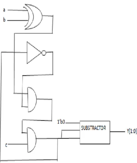
As stated above CSD is also done directly using the consecutive iteration method and bit by bit method. But the bit by bit method conversion is systematically modeled and easily designed by considering the following block diagram Fig 1.
An Optimized Area Efficient High Speed CSD
Multiplier for Image Processing Applications
Fig 1: Bit by bit CSD converter block diagram.
Fig 2: CSD converter for 4 bits
The above circuit represented in Fig 2 is used for n number of required bits. Thus we can convert a number from its binary form to CSD representation. Mainly converting a number from binary to CSD will reduce the number of consecutive ones. This leads to reduction in number of computations and additions required for implementation. Thus CSD algorithm can be used in Image processing applications which reduces the final computation time. In this paper the main outcome is one of the image processing application which is edge detection.
In this paper CSD multiplication between multiplicand (m) and multiplier (p) is done by considering an image pixel values of size 3 X 3 matrix. For an image, pixel values of size 3 X 3 matrix is chosen by using MATLAB software and
assumed it to be a multiplicand(m) .Another kernel matrix of size 3 X 3 is chosen as multiplier which can be used for edge detection for an image processing applications. In general it is known that in order to enhance the image convolution between image matrix and kernel matrix is done which involves multiplication as one of the intermediate operation.
m =
3
1
2
4
7
6
8
5 10
---(3)
The kernel matrix (b) is chosen as multiplicand
p=
0
1
0
1
4
1
0
1
0
---(4)
In order to implement the digital multiplier for an obtained image matrix and kernel matrix, each pixel values of both matrices are represented into binary values of 4 bits each of size 3 X 3 matrix and CSD multiplication between image matrix and kernel matrix is done in order to increment the performance and results are measured with Dadda multiplier with respect to speed and area using Xilinx ISE tool. CSD matrix is usually represented using three bits which are 0,1 and 1' (minus one). For few 4-bit binary data CSD representation may not change. As an example consider one of pixel value from a multiplicand matrix (a) let it be 7. It's binary representation is 0111 and its CSD representation is defined as 1001' which gives the value of 7, where as for pixel value of 1 the binary and CSD representation is same, doesn’t change. Hence converting a number from binary to CSD representation will give the faster result with less calculations and computations.
Ex: 0111 ---- 0X23 + 1X22 + 1X21 + 1X20 = 7 ---- 1X23 + 0X22 + 0X21 - 1X20 = 7
III. DADDA MULTIPLIER
[image:2.595.59.279.49.310.2] [image:2.595.83.225.338.610.2]
International Journal of Innovative Technology and Exploring Engineering (IJITEE) ISSN: 2278-3075, Volume-8 Issue-7, May, 2019
It is possible to make an circuit utilizing a few full adders to include multiple bit numbers. Each full adder inputs a Cin, which is the Cout of the previous adder. This sort of adders is a ripple adders , since each carry bit ripples to the following full adder. Carry save adder is an another approach used to incorporate more number of summations to be accomplished with the Cin and Cout parallel in creating the partial products.
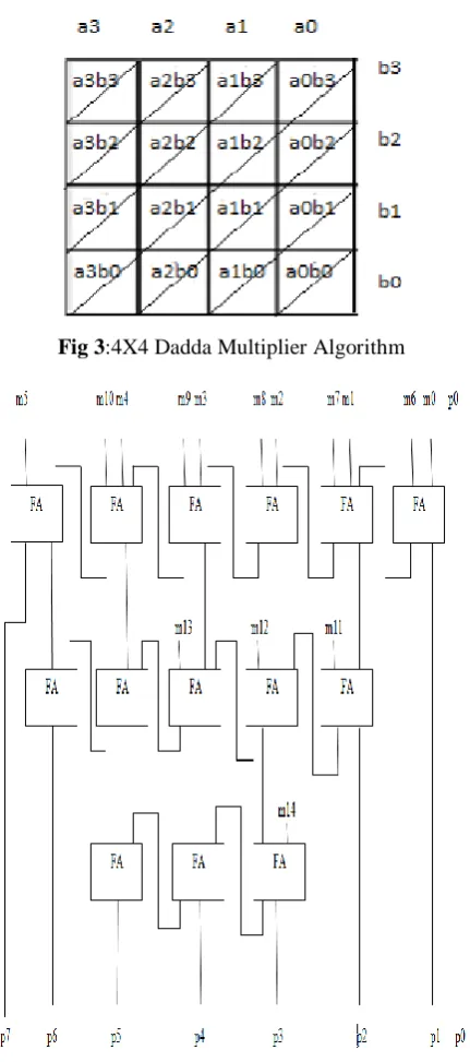
The calculation of DADDA multiplier depends on the underneath grid structure appeared in Figure. The incomplete item network is framed in the principal organize by AND stages which is delineated.
Fig 3:4X4 Dadda Multiplier Algorithm
Fig 4: Dadda Multiplier Block Diagram
Fig 4 shows the block diagram of Dadda multiplier where 4-bit multiplicand and multiplier bits are given as inputs and multiplication is performed. Obtained intermediate partial
products are given to full adder for computing final partial products and carry is propagated to next successive full adders and so on. Thus final partial products of 8 bits is obtained. In this paper image pixel values and kernel matrix are given as inputs to the 4 X 4 Dadda multiplier. Hence in order to improve the speed of operation instead of giving binary inputs ,they are converted into CSD form and given as inputs to a Dadda multiplier and therefore delay, area is computed.
IV. VEDIC MULTIPLIER
The utilization of Vedic arithmetic lies in the way that it diminishes the commonplace counts in traditional science to extremely basic ones. This is so on the grounds that the UT Vedic approach are professed to founded on the characteristic standards on the human personality works. Vedic Maths is a system of number juggling decides that permit increasingly proficient speed execution. This is a fascinating field and shows some compelling calculations which can be connected to different parts of designing, for
example, processing. From the ancient Indian Vedas,
another old number juggling was re found and called as Vedic science in mid twentieth century. The phrase 'Vedic' is gotten from the phrase 'veda' that suggests learning. Period of Vedic starts from 300BC. Vedic System duplicated some place in the scope of 1911 and 1958 Bharati Krishna thought of one essential motivation in 1958 "Vedic Mathematics" circulated in 1965. IJET Multiplier is one of the key gear used in most of the applications. Multiplier on its own is having monstrous job with colossal postponement of intensity scattering.
In this manner for quick processors, image processing applications and for DSP applications a rapid multiplier is useful for better execution as multipliers are used by and large in Chip, Digital signal processing and Communication applications. By using Vedic multiplier, speed of computation can be improved figuring most of the DSP applications. Multipliers can be arranged by using phenomenal adders as full adders, carry select adders and Manchester adders. In this paper for increment a methodical Vedic multiplier is using Urdhava Tiryagbhyam. this Vedic multiplier includes less computations and performs speed operations among the all multipliers.
[image:3.595.62.278.224.711.2] [image:3.595.315.540.585.831.2] [image:3.595.316.527.600.726.2]Every individual square in the Fig 5 is a 2X2 multiplier.
Fig 6: 2X2 multiplier
A 2X2 multiplication is done for each square box represented in Fig 6 and all intermediate partial products are assumed to be i(0-15) . In order to obtain final result, the output of each 2X2 multiplier blocks are rearranged as shown in fig below and addition operation is performed among the intermediate partial products to get a final result.
Fig 7: Final output of 4-bit multiplier
In this paper 4 bit Vedic multiplier is designed for a 4bit CSD input. First the 4 bit input is divided into 2 bits and the intermediate products are generated. Now these intermediate products are represented as variable i0-i15.These intermediate products are arranged in a particular order as mentioned in above figure. Finally the multiplier output is represented as r0-r7 by computing the intermediate partial products using adder.
V.SIMULATION RESULTS
Fig 8: Input image matrix
Fig 8 describe about the input image matrix first row [ 3 1 2 ] (i.e. equation 3) which are represented from m0-m11 each of 4-bits.
Fig 9: Input Kernel
Fig 9 describes about the edge detection kernel first column [ 0 1 0 ] (i.e. equation 4) which are represented from p0-p11 each of 4-bits.
Fig 10: Result of multiplier
Fig 10 describe about the result of multiplication of Image matrix with Kernel represented with k10-k17 i.e. multiplier output of Dadda and UT Vedic which is to be 1 from Fig 8 and Fig 9.
[image:4.595.314.538.49.188.2] [image:4.595.66.269.77.183.2] [image:4.595.313.540.223.364.2] [image:4.595.51.264.303.499.2] [image:4.595.309.543.387.505.2] [image:4.595.314.538.548.755.2]International Journal of Innovative Technology and Exploring Engineering (IJITEE) ISSN: 2278-3075, Volume-8 Issue-7, May, 2019
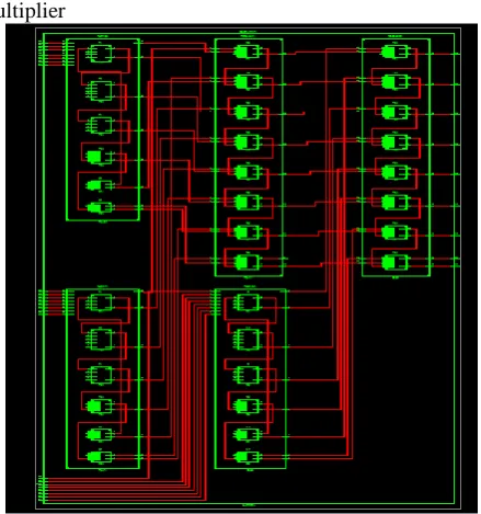
Fig 11 describe the RTL Schematic diagram of UT Vedic Multiplier
Fig 12: Schematic of Dadda Multiplier
Fig 12 describe the RTL Schematic diagram of Dadda Multiplier.
VI. CONCLUSION
From the table shown below and the observation of above results of matrix multiplication with both Dadda Multiplier and UT Vedic Multiplier using CSD technique, UT Vedic Multiplier will produce fast (i.e. less delay) output with less area utilization which can be used for image processing applications like edge detection and can be further implemented using FPGA for high speed operations.
UT CSD MULTIPLIER
DADDA CSD MULTIPLIER
Delay 4.330ns 5.935ns
No of LUT’s
60 out of 63400 70 out of 63400
No of IO’s
33 out of 210 33 out of 210
REFERENCES
1. Lakshmi kiran Mukkara, K.Venkata Ramanaiah “A Simple Novel Floating Point Matrix Multiplier VLSI Architecture for Digital Image Compression Applications”, International Conference on Inventive Communication and Computational Technologies (ICICCT2018), ISBN:978-1-5386-1974-2
2. M.Lakshmi Kiran and Dr. K.Venkata Ramanaiah, “ Implementation of High Speed and Low Area Digital Radix-2 CSD Multipliers using Pipeline Concept”, International Journal of Electronics and Communication Engineering. ISSN 0974-2166 Volume 10, Number 1 (2017), pp. 53-61 3. Michael A. Soderstrand, “CSD MULTIPLIERS FOR FPGA DSP
APPLICATIONS”, 0-7803-776 1-31031$17.00 02003 IEEE
4. Navdeep Goel and LalitGarg, “Comparative Analysis of 4-bit CMOS
Multipliers”, Proceedings of International Conference on VLSI,
Communication & Instrumentation, pp. 33 – 37, 2011.
5. C.Priyanka, N.Manoj Kumar, “ Low power and high speed GDI based
convolution using Vedic multiplier”, International Journal of Engineering & Technologgy, 7 (2.7) (2018), 733-738
6. R.Uma, Vidya Vijayan , M. Mohanapriya, Sharon Paul, “Area, Delay and
Power Comparison of Adder Topologies”, International Journal of VLSI
design & Communication Systems, vol.3, No.1,pp.153-168, February 2012.
7. Saroja.V Siddamal, R.M.Banakar and B.C.Jinaga “Design of High-speed
floating point multiplier”,in the 4th International Sympoiusm on Electronic Design, Test And Applications,China,2008.
8. C. Jaya Kumar and R. Saravanan “VLSI Design for Low Power Multiplier
using Full Adder”, European Journal of Scientific Research, vol.72, no.1, pp. 5-16, March 2012.
9. Jang, J.W., S.B. Choi, V.K.Prasanna, 2005. “Energy and time efficient matrix multiplication on FPGAs,” IEEE Transactions on Very Large Scale Integration Systems VOL. 13, NO. 11, APRIL 2005.
10. AmritaNanda,”Design and Implementation of Urdhva-Tiryakbhyam
Based Fast 8×8 Vedic Binary Multiplier”IJERT, ISSN: 2278- 0181,Vol. 3 Issue 3, March – 2014
11. Poornima M, Shivaraj Kumar Patil, Shivukumar, ShridharKP,Sanjay H,
“Implementation of Multiplier Using Vedic Algorithm”, JITEE, ISSN:-2278-3075, Volume-2, Issue-6,May-2013.
12. Rui Guo and Linda Sumners DeBrunner, “A novel fast
canonical-signed-digit conversion technique for multiplication,”in Proc. ICASS,pp.1637-1640, 2011.
13. Premananda B.S, Samarth S. Pai, Shashank B, ShashankS.Bhat, “Design
and Implementation of 8-bit Vedic Multiplier”, IJAREEIE, Vol.2, Issue 12, ISSN: 2320-3765, Dec-2013
14. Anju& V.K. Agrawal,”FPGA Implementation of Low Power and High
Speed Vedic Multiplier using Vedic Mathematics”, IOSRJVSP , e-ISSN: 2319 – 4200 ,2, Issue 5 (May. – Jun. 2013), PP 51-57
15. A. Kanhe, S. Das, and A. Singh, “Design and implementation of floating
point multiplier based on vedic multiplication technique,” in Communication, Information Computing Technology (ICCICT), pp. 1–4, 2012.
AUTHORSPROFILE
C.Priyanka Assistant Professor,
Department of ECE, Koneru Lakshmaiah Education Foundation,
Vaddeswaram ,Guntur,Andhra Pradesh,India.
E.RanaPratap is studying B. Tech in Electronics and Communication Engineering in Koneru Lakshmaiah Education Foundation, Vaddeswaram, Guntur, Andhra Pradesh, India.
S.Bhaskar is studying B. Tech in Electronics and Communication Engineering in Koneru Lakshmaiah Education Foundation, Vaddeswaram, Guntur, Andhra Pradesh, India.
[image:5.595.58.278.64.299.2] [image:5.595.44.295.456.561.2]