Bottom-up Silicon Nanoelectronics
Hiroshi. Mizuta*1,6, Mohammed Khalafalla3,6, Zahid A.K. Durrani3,6, Shigeyasu Uno4,6, Nobuyoshi Koshida5,6, Yoshishige Tsuchiya2,6 and Shunri Oda2,6
1Department of Physical Electronics, Tokyo Institute of Technology, Tokyo, Japan 2Quantum Nanoelectronics Research Center, Tokyo Institute of Technology, Tokyo, Japan
3Microelectronics Research Centre, University of Cambridge, Cambridge, UK 4Hitachi Cambridge Laboratory, Hitachi Europe Ltd., Cambridge, UK
5Faculty of Technology, Tokyo University of Agriculture and Technology, Tokyo, Japan 6 CREST, JST (Japan Science and Technology)
*Email: [email protected]
Abstract
This paper presents an overview on recent topical studies on electronic properties and device applications of silicon nanodots as a bottom-up building block for silicon nanoelectronics. The electrostatic and quantum-mechanical interactions in double Si nanodots, the phononic states and electron-phonon interactions in the linear chain of Si nanodots covered with thin oxide layers, and the non-volatile nanoelectromechanical memory device incorporating Si nanodots are discussed.
1. Introduction
Over the past few decades, the performance of silicon-based VLSI circuits has steadily been improved by scaling down device dimensions, and a nearly exponential growth of microelectronics capabilities has been achieved. However, maintaining this top-down miniaturization trend is getting exceedingly hard due to fundamental physical and technological limitations as well as of the economical limitation although an experimental nanoscale MOSFET with the gate length down to 10 nm has been demonstrated. On the other hand, the use of organic molecules as a building block for nanoscale devices has attracted much attention since the precisely controlled nanostructures may be formed cheaply by utilizing self-assembly of molecules. This bottom-up technology can potentially overcome the inherent problem of the present silicon top-down technology. The conductivity of the organic molecular structures is, however, still much lower than those for silicon as the electron transport along the single molecule is basically governed by the hopping conduction.
Silicon nanodots and nanowires [1]-[4] may provide a solution to these issues by meeting the requirements both of bottom-up organization and superior carrier transport properties. As those silicon nanostructures can be formed
on non-Si substrates such as glass and plastic, the Si-based bottom-up approach may lead to high-performance and large-area electronics. In addition, zero- and one-dimensional nature of electronic states in the individual Si nanodots and nanowires realizes new electronic and photonic properties which are not achieved with bulk silicon. Combining the bottom-up approach with the conventional top-down Si technologies enables us to explore silicon nano-, micro- and macro-electronics on the common technical footing.
Fig. 2 Combination of top-down and bottom-up approaches for silicon nanoelectronics
1μm 1μm
TOP
TOP--DOWN DOWN SiSi
BOTTOM
BOTTOM--UP UP SiSi
1μm 1μm
TOP
TOP--DOWN DOWN SiSi
BOTTOM
BOTTOM--UP UP SiSi Fig. 1Atomic structures of (a) a silicon nanodot (Si29H24) and (b) a silicon nanowire (Si336H250) calculated using the SIESTA package [5][6].
[image:1.595.308.542.242.338.2] [image:1.595.320.509.506.672.2]This paper focuses on the silicon nanodots and presents recent topical studies on their nanoscale electron transport properties and device applications. For fabricating Si nanodots we have studied three different techniques. The first method is to use a very thin nanocrystalline (nc) Si film with the size of the grains down to a few nanometer. The nc-Si films can be formed either from an amorphous Si film with solid phase crystallization (SPC) or by using a very high frequency (VHF) plasma-enhanced chemical vapour deposition (PECVD) at a low temperature [7]. In the SPC films the individual grains are usually columnar shaped, and the grain boundaries (GBs) between adjacent grains contain carrier trap states due to dangling bonds. On the other hand, in the PECVD films, the individual grains are more spherical, and the GBs are formed by a-Si:H layers between grains. The second approach is to use porous Si [8] formed by using photoanodization of the Si substrate. The surface of the nc-Si islands formed in the substrate can be oxidised selectively by electrochemical oxidation. Formation of a linear chain of nc-Si islands with a diameter as small as 5 nm has been observed [9]. The third approach is a VHF plasma enhanced deposition of silane with a hydrogen gas pulse sequence [10]. This technique facilitates in separating the nucleation and crystal growth process and helps to fabricate nc-Si particles with diameter less than 10 nm and dispersions of 1 nm [11]. Particle diameter down to 3 nm has also been reported recently [12]. The interparticle tunnel barriers can be formed by in-situ oxidation or nitridation in a controlled manner.
In the following sections, we discuss three recent topics on the electron transport properties and device application of the Si nanodots: the electrostatic and quantum-mechanical interactions in double Si nanodots (Section 2), the phononic states and electron-phonon interactions in the linear chain of Si nanodots covered with thin oxide layers (Section 3), and the non-volatile nanoelectromechanical memory device incorporating Si nanodots (Section 4).
2. Inter-dot coupling effects in nc-Si SETs
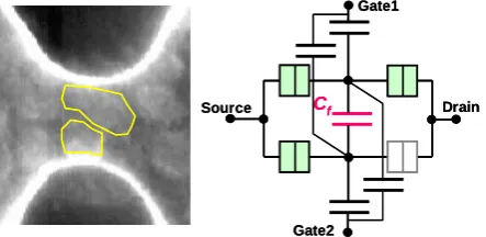
Electrostatic and coherent coupling effects between two adjacent nc-Si grains were studied by using point-contact single-electron transistors (PC-SETs: Fig.3 (left)). The PC-SETs with a very small channel with 30 nm × 30 nm in lateral dimensions were formed on a 40 nm thick nc-Si film with lateral grain size of 20 – 25 nm. The electrostatic potential on the grains are controlled via the bias applied to two side gates. After patterning the PC-SETs, oxidation at 750°C for 60 minutes and annealing at 1000°C were applied, which convert the
grain boundary (GB) into a solid tunnel barrier [13]. We observed the switching of the Coulomb oscillation current peaks at 4.2K as we swept the two side gate voltages Vg1 and Vg2 (Fig. 3 (right)) [14], and the phenomenon was successfully reproduced using the Monte Carlo single-electron circuit simulation with a model of two parallel, capacitively-coupled Si nanodots (Fig. 4).
Next we adopted oxidation at 750°C for 30 minutes without the following annealing in order for making the GB tunnel barrier more transparent so that the adjacent grains couple each other more tightly. The PC-SETs then exhibited delocalisation of the electron wavefunctions over the coupled grains. A plot of the device conductance at 4.2 K as a function of the two side gate voltages (Fig. 5) shows single-electron conductance peaks which partially form an electron stability diagram for two charging grains [15]. The peak lines in this plot (white dotted lines) show strong splitting (a dotted circle) caused by electrostatic interactions when the
Source Drain
Gate2 Gate1
Cf
Source Drain
Gate2 Gate1
Cf
Fig. 4 A blow-up of the point-contact channel with two parallel Si grains indicated by thin lines (left) and an equivalent circuit for the capacitively coupled double parallel dots (right)
150 n
m
Vg1
Vg2
-4 -3 -2 -1 0 1 2 3 4 -4
-3 -2 -1 0 1 2 3 4
Vg1(V)
Vg2
(V
)
Source Drain Gate2
Gate1
[image:2.595.313.541.173.304.2] [image:2.595.310.532.392.500.2]energy levels in the two grains are in resonance. In this strong coupling region, we observed that the characteristics are decomposed into four Lorentzian peaks – two main peaks with two small peaks. This is attributed to the tunnel coupling across two adjacent Si grains, resulting in bonding- and anti-bonding-like resonance peaks [16].
3. A novel building block for Si multifunctional device
Silicon and its oxides, the key players in the LSIs, now combine in a different way to offer new functional applications in electronics and mechanics. Electron transport properties of the Si nanodots interconnected with thin oxide layers have recently attracted growing attention due to the experimental observation of ballistic electron emission [17]. We investigate the electronic and phononic states in a one-dimensional array of Si nanodots interconnected with thin oxide layers (1DSiNDA) as shown in Fig. 6. This system has wide variety of interesting features such as phonon bandgap, phonon confinement, reduction of electron-phonon scattering potential, and strong energy loss suppression.
Figures 7(a) and 7(b) show phonon energy dispersion relationship and phonon density of states. Note that there
are energy ranges at which phonons do not exist [18]. This indicates that 1DSiNDA acts as ‘lattice vibration filter’, which filters out the vibrations having the energy in the phonon bandgap. Changing the thickness of the oxides controls the energy range of the bandgap. It is also interesting to note that the energy dispersion for high-energy phono ns is flat. Such phonons are confined in Si nanodots.
Another interesting feature of the 1DSiNDA is the reduction of the electron-phonon scattering potential, which is written as
where S(x) and Daco denote phonon wave function and the coupling constant, respectively. The first derivative of S(x) is also know as the strain. Fig. 8 compares the
strain in the 1DSiNDA (open circles) and conventional Si quantum wire (broken line). Note that the oxide layers ‘absorb’ the strain from the Si nanodots [18]. This is reasonable because the oxide layers are ‘softer’ than Si nanodots (the Young’s modulus of Si and oxide are
Fig. 7 (a) Phonon energy dispersion in 1DSiNDA (b) Phonon density of states calculated from (a).
Fig. 6 Schematic illustration of the1DSiNDA.
2.0
1.0
0
-1.0
-2.0
-3.0
0 2.0 4.0
-4.0 -2.0
Vg1(V)
Vg2
(V
)
Vds= -2 mV
T = 4.2 K
2.0
1.0
0
-1.0
-2.0
-3.0
0 2.0 4.0
-4.0 -2.0
Vg1(V)
Vg2
(V
)
Vds= -2 mV
T = 4.2 K
Fig. 5 A gray scale image of current as a function of two side gate bias voltages Vg1 and Vg2 for the PC-SET with tunnel-coupled double Si nanodots
( )
( )
el-ph aco
,
(1)
S x
H
x
D
x
∂
=
∂
[image:3.595.71.244.175.313.2] [image:3.595.317.515.177.319.2] [image:3.595.309.549.566.683.2] [image:3.595.62.280.569.645.2]180GPa and 70GPa, respectively). As the coupling constant Daco in the oxide is smaller than that in Si, the strain absorption effect reduces the scattering potential over the entire region in 1DSiNDA compared to that of Si quantum wire. This may lead to a significant reduction of electron-phonon scattering.
The electron energy loss is also suppressed in the 1DSiNDA [19]. Fig. 9 shows the electron energy loss per unit time caused by the phonon scattering in the 1DSiNDA, calculated for an electron miniband. Note that the energy loss rate is significantly suppressed at the vicinity of the miniband bottom energy. Thus, the electron energy loss becomes much less than that in the Si nanowires.
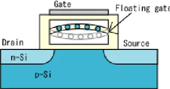
4. Si nanodot nonvolatile nanoelectromechanical memory
Silicon-based nano Electro-Mechanical Systems (NEMS) have recently been of great interest from stand-points of their extremely high-speed operation [20] as well as physics of electron transport coupled with a nanoscale mechanical resonator [21][22]. We recently proposed a new nonvolatile memory concept based on bistable operation of the NEMS structure combined with the Si nanodots (Fig.10). Our NEMS memory features a suspended floating gate beam in the cavity placed under the gate electrode, which contains the Si nanodots as charge storage. The floating gate is bent naturally, either upward or downward, and its both ends are clamped at the cavity side walls. When the gate voltage is applied, the floating gate beam moves via electrostatic interactions between the gate electrode and the charge in the Si nanodots. The switching speed between two stable states was estimated to be ~ 0.5 ns for a SiO2 beam with the dimension of 1.0 × 1.0 × 0.1 μm3, from a mechanical analysis assuming the maximum central displacement of 35 nm.
A positional displacement of the floating gate may be sensed with a change in the drain current of the MOSFET underneath. Mechanical bistablity of the beam is therefore essential for achieving our non-volatile NEMS memory, and a higher switching speed is expected with reducing their dimensions down to the nanometer regime. As the switching mechanism does not depend on any charge tunneling through the gate oxide, we may avoid the gate oxide degradation, which is one of the serious issues in the conventional flash memory.
Mechanical properties of the beam were analyzed by using a parallel three-dimensional (3D) finite element simulation [23]. A nc-Si beam structure, in which a two-dimensional array of Si nanodots are embedded in a SiO2 film (Fig. 11(a)), was compared with a simple poly-Si beam structure, in which a thin Si sheet are placed between SiO2 layers. The Young’s modulus and Poisson’s ratio of 190 GPa and 0.27 for Si, and 70 GPa and 0.175 for SiO2 were used for the present simulation. Calculated 3D images of the beam deformed under a constant homogeneous pressure parallel to Z-axis are shown in Fig. 11(b). The maximum central displacement obtained for the nc-Si beam was found larger than that for the poly-Si beam with the same pressure. This indicates that a larger displacement is achievable for the nc-Si beam structure under the same external electric filed and, therefore, the nc-Si beam has an advantage for low power operation.
[image:4.595.330.505.204.295.2](a) (b)
[image:4.595.61.277.259.389.2]Fig. 11 A SiO2 beam incorporating Si nanodots used for 3D FE simulation (a) and the deformed beam under an applied uniaxial force (b).
Fig. 10 A schematic cross-sectional view of a NEMS memory device.
Fig. 9 Energy loss rate in the 1DSiNDA and Si quantum Si nanowire
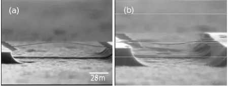
[image:4.595.314.541.562.645.2]In order for investigating the mechanical properties of beam structure experimentally, the nano-indentor type loading system [24] was used. For this experiment, a single layer SiO2 beam structure was fabricated using a dry etching Si undercut technique (Fig. 12 (a),(b)). The most of the fabricated samples showed an upward bent beam as shown in Fig. 12(a), and this is considered as a result of release of mechanical stress stored in SiO2 after removing a Si layer underneath. However, few samples showed a downward bent beam (Fig. 12(b)), and this fact indicates that the beam has a mechanically bistable states. We loaded the upward bent beam with the tip of the nano-indentor around the center of the beam. After the loading we observed that the beam was switched to the downward bend position, and this confirms that the bistable states can be switched by applying an external force.
5. Summary
We overviewed recent topical studies on electronic properties and device applications of Si nanodots as a bottom-up building block for nanodevices. We first discussed the electrostatic and coherent coupling of electronic states in double Si nanodots interacting each other. Single-electron conductance peaks are seen at 4.2 K as a function of two gate voltages, caused by electrostatic coupling between the Si nanodots. Additional conductance peaks are observed when the energy levels from two adjacent nanodots are resonant. These peaks may be associated with ‘quasi-molecular’ states formed by coherent coupling of the energy levels in the nanodots. Secondly, we theoretically studied electronic and phononic states in the 1D silicon/oxide heterostructure. The results showed that the phonon emission rate is larger than the one calculated for Si quantum wire, while the energy loss rates at near the bottom of minibands are much smaller, showing energy ranges at which energy loss is strongly suppressed. Thirdly, we investigated a new non-volatile NEMS memory device with the Si nanodots embedded in a movable floating gate beam. Advantage of using the Si nanodots array for the movable floating gate beam was shown for low power operation. The mechanical
bistability of the fabricated SiO2 beam was clearly observed.
Acknowledgments
The authors are very grateful to Mr. K. Takai, Mr. N. Momo, Mr. K. Usami, Mr. S. Higashijima, Mr. Y. Kurokawa of Tokyo Institute of Technology for their valuable technical contributions, and Dr. T. Shimada, Dr S. Yamaguchi, Dr. S. Saito, Dr. Arai of Central Research Laboratory, Hitachi Ltd., Prof. K. Nakazato of Nagoya University, Prof. N. Mori of Osaka University, Dr. T. A. Armour of Nottingham University for very useful discussions.
References
[1] Y. Cui and C. M. Lieber., Science 291, 851 (2001) [2] Y. Huang et al., Science 291, 630 (2001)
[3] X. Duan et al., Nature 425, 274 (2003)
[4] S. Piscanec et al., Phys. Rev. B68, 241312 (2003)
[5] P. Ordejon et al., Phys. Rev. B53, R10441 (1996)
[6] J. M. Soler et al., J. Phys.: Condens. Matt. 14, 2745
(2002)
[7] T. Kamiya et al., J. Appl. Phys. 89, 6265 (2001) [8] N. Koshida and H. Koyama, Appl. Phys. Lett. 60,
347 (1992)
[9] A.G. Cullis et al., J. Appl. Phys. 82, 909 (1997) [10] S. Oda and M. Otabe, Mater. Res. Soc. Proc. 358,
721 (1995)
[11] T. Ifuku et al., Jpn. J. Appl. Phys. 36, 4031 (1997)
[12] J.De Blauwe, et al., IEDM Tech. Dig., 683 (2000)
[13] Y. T. Tan et al., J. Appl. Phys. 94, 633 (2003)
[14] M. Khalafalla et al., IEEE Nanotech. 2, 271 (2003).
[15] W G van der Wiel, et al., Rev. Mod. Phys., V. 75(1),
1 (2003).
[16] R H Blick et al., Phys. Rev. Lett., V. 80 (18), 4032
(1998).
[17] N. Koshida et al., Appl. Surf. Sci., 146, 371 (1999).
[18] S. Uno et al., IEEE Trans. Nanotechnol. 2, 301
(2003)
[19] S. Uno et al., Silicon Nanoelectronics Workshop,
Honolulu, (2004)
[20] X.M.H. Huang et al., Nature 421, 496 (2003).
[21] E. M. Weig et al., Phys. Rev. Letts. 92, 046804
(2004)
[22] A. D. Armour et al., Phys. Rev. B69, 125313 (2004)
[23] http://www.j-insight.com/ & http://adventure.q.t.u- tokyo.ac.jp/
[24] K. Takashima et al., Mat. Trans. 42, 68 (2001).
(a) (b)
[image:5.595.59.286.278.363.2]2μm
![Fig. 1 Atomic structures of (a) a silicon nanodot (Siand (b) a silicon nanowire (Si29H24) 336H250) calculated using the SIESTA package [5][6]](https://thumb-us.123doks.com/thumbv2/123dok_us/8519573.352651/1.595.320.509.506.672/atomic-structures-silicon-nanodot-silicon-nanowire-calculated-package.webp)