Int. J. Electrochem. Sci., 14 (2019) 3434 – 3442, doi: 10.20964/2019.04.20
International Journal of
ELECTROCHEMICAL
SCIENCE
www.electrochemsci.org
Short Communication
Fabrication of a Microstructure Array Using Electrochemical
Wet Stamping Technique with a Polyacrylamide Gel
Dao-Peng Xia, Lei-Jie Lai*
College of Mechanical & Automotive Engineering, Shanghai University of Engineering Science, Shanghai 201620, China.
*E-mail: [email protected]
Received: 5 December 2018 / Accepted: 14 January 2019 / Published: 10 March 2019
A new micromachining method known as the electrochemical wet stamping technique (E-WETS) is presented in this paper for the fabrication of 3D microstructure arrays on material surfaces. In the E-WETS, a prepatterned polyacrylamide gel template serves as the channel for electrolyte and current flow between the workpiece anode and the tool cathode. The microstructures are fabricated through the limitations of selective anodic dissolution in the contact area between the workpiece and the gel template. Based on the characteristics of the E-WETS, a complete set of micromachining instruments, primarily consisting of a macro-micro positioning stage, are developed. The potential of the short pulse is exploited to increase the precision of the fabricated microstructures. Under the optimized conditions, two complex microstructure arrays are successfully fabricated on a nickel surface. The machining deviations of the two fabricated microstructures from those on the stainless-steel moulds are only 1.02% and 1.12%, respectively. The machining results demonstrate that the E-WETS method is a promising approach for fabricating microstructure arrays with high fidelity and accuracy.
Keywords: Electrochemical wet stamping technique, Microstructure array, Polyacrylamide gel template, Short pulse
1. INTRODUCTION
attention due to its ability to produce complex structures of metal materials without tool wear and stress, whether the metal is heat-resistant, high tension or high strength [4].
In recent years, many EMM technologies have been developed. Schuster et al. used nanosecond ultra-short pulses to restrict the space range of the electrochemical reactions [5, 6]. A confined etchant layer technique (CELT) was developed by Tian, by confining the etchant near the mould surface with complicated micropatterns [7, 8]. However, when the tool electrode is close to the workpiece, both methods encounter difficulties in exchanging the product or electrolyte with the bulk solution [9]. Landolt et al. studied a new EMM method that combined lithography and electrochemical techniques, by using a photoresist applied to the workpiece surface to serve as a barrier in order to achieve the desired structures [10]. However, accurate shape control of the microstructure in these methods is difficult to realize. Accordingly, it is necessary to develop a new and efficient EMM technology for microstructure fabrication.
A new electrochemical micromachining method, called the electrochemical wet stamping technique (E-WETS), is proposed here for the preparation of three-dimensional microstructure arrays. Zhang et al. first presented E-WETS and used it for micromachining on various material surfaces [11– 14]. In E-WETS, because the electrolyte is constantly supplied by the gel template to the interface, a patterned agarose template is used to limit electrochemical reactions to occurring only in the contact area. E-WETS successfully solved the difficulty of electrolyte exchange between the product and bulk solution when the workpiece is close to the gel template. However, one drawback of E-WETS is that only convex microstructures can be fabricated on the workpiece due to the low strength of the agarose template. Additionally, the agarose gel, which is a linear polymer hydrogel with several ten-micrometre holes, limits the fabrication accuracy of E-WETS. Here, instead of agarose gel, a polyacrylamide gel serves as the gel template for fabricating the microstructure. In comparison with agarose gel, polyacrylamide gel has the advantages of a more porous structure and higher strength. The former improves the transportation efficiencies of the electrolyte and product, while the latter enables the gel template to resist deformation and damage under certain pressures. In this paper, a new E-WETS technique based on polyacrylamide gel is studied for fabricating microstructure arrays on a material surface. Using short voltage pulses, we produced sophisticated microstructures with excellent shape precision on a metal surface, validating the effectiveness of the E-WETS.
2. EXPERIMENTAL
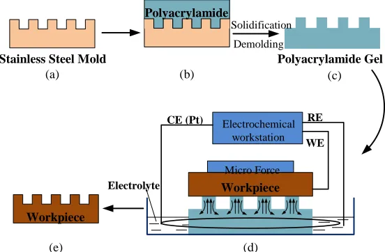
Fig. 1(b) shows that the micropatterned polyacrylamide gel template was prepared by casting a mixed solution of monomer (acrylamide, Acr), crosslinker (bis), initiator (APS) and catalyst (TEMED) onto a stainless-steel mould. The mass ratio of the composition of the polyacrylamide gel was optimized to be 16% monomer + 0.6% crosslinker + 0.5% initiator + 0.05% catalyst. The stainless-steel mould used here was produced by a chemical etching technique. After curing for 2 h, the polyacrylamide gel was carefully peeled off from the stainless-steel mould, and complementary microstructures were obtained on one side of the polyacrylamide gel. Subsequently, we immersed the gel template in an aqueous electrolytic etching solution for 1 h. Before use, the polyacrylamide gel template was placed on filter paper for 8 min, and nitrogen was passed over the gel for 100 s to remove excess electrolyte on the template surface. This procedure can limit the lateral expansion of the etching solution during microfabrication.
Electrochemical micromachining was carried out in a homemade three-electrode electrochemical cell (Fig. 1(d)). An electrochemical cell filled with electrolyte was provided with the gel template at the bottom of the cell with the patterned side facing up.
Figure 1. The E-WETS principle and process.
The solution should not immerse the surface of the gel template. The unpatterned side of the gel template was partially submerged into the solution. The workpiece was subsequently placed on the gel template to serve as the working electrode (WE). A saturated calomel electrode (SCE) and a Pt wire served as the reference electrode (RE) and the counter electrode (CE), respectively. By using an electrochemical workstation (CHI 760D from CH Instruments), we performed all potential control and electrochemical measurements. To control the potential of the WE versus the SCE, we applied a high-frequency pulsed voltage by a pulsed power supply (SHD2-DMC15/10 from Shijiazhuang Sihang Electronic Technology Co., Ltd., Shijiazhuang, China) in the electrochemical workstation [9]. During the machining process, a constant micro-force was applied to maintain contact between the workpiece and template, and the gel template was etched into the workpiece step by step. Fig. 1(e) shows that a microstructure similar to that of the stainless-steel mould can be made on the workpiece. The
Demolding
Stainless Steel Mold
Polyacrylamide Polyacrylamide Gel Solidification Micro Force Workpiece Workpiece Electrolyte b
( a ) ( ) ( c )
) ( d ( e )
Electrochemical workstation WE
[image:3.596.159.435.326.507.2]
microstructures of the stainless-steel mould and the fabricated workpiece were characterized under a metallographic microscope (RH-SM-10A from Yuyao Dagong Instrument Co., Ltd., Ningbo, China).
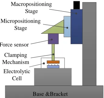
[image:4.596.214.385.359.519.2]According to the characteristics of the E-WETS process, an electrochemical micromachining device was developed [9, 15]. Fig. 2 provides a schematic diagram of the device developed for the E-WETS. This device primarily comprises a macro-positioning stage, micro-positioning stage, clamping mechanism, force-sensing module, electrolytic cell, base and bracket. The z-directional motion stage is a critical component for accurate positioning and movement of the workpiece relative to the gel template [9]. The z-directional motion stage adopts a macro-micro dual-drive positioning method, including a macro-micro positioning phase and a micro-positioning phase, to obtaining high positional accuracy over a large range of motion. The macropositioning stage is primarily composed of a cross-roller guide, a pre-loaded ball screw and a stepping motor, which can realize a wide range of rapid approaches of the processed workpiece to the gel template. The micro-positioning stage is a flexure-based compliant mechanism driven by a piezoelectric actuator, which can realize precise micro-displacement positioning of the processed workpiece on the gel template. For the detection and control of the contact force between the gel template and the workpiece, a force sensing module is used, which can compensate for a decrease in the force as the workpiece is dissolved by the template.
Figure 2. A schematic of the micromaching instrument.
3. RESULTS AND DISCUSSION
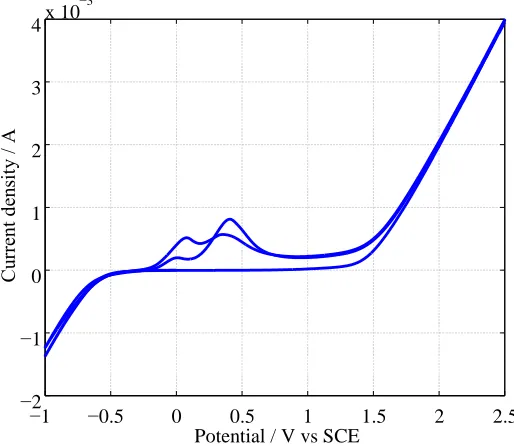
A gel template with a microstructure array was fabricated as shown in Fig. 3. The machining material for the E-WETS in this paper was chosen to be nickel, and the etching solution for the electrochemical micromachining of nickel was an aqueous solution that contained 10% Na2SO4, 5% H3PO4, 1% glycerin and 1% tartaric acid. A cyclic voltammogram of a Ni workpiece on the micropatterned gel template immersed in the solution is shown in Fig. 4. This voltammogram shows characteristic areas of passivity, passivation, active dissolution and transpassivity, corresponding with an increase in the anode potential [16]. In the curve shown in Fig. 4, the current peak of 0.4 V represents the passivation and dissolution of Ni. When this potential is exceeded, the dissolution rate shows a dramatic decrease. In the passivity region of 0.6−1.2 V versus SCE, the anodic current
Base &Bracket Macropositioning
Stage
Micropositioning Stage
Clamping Mechanism
decreases to be very low, dissolving stops, and micromachining does not occur. As the potential becomes more positive (>1.2 V versus SCE), transpassivation of Ni appears, and oxygen is evolved simultaneously.
Figure 3. Microscope image of the microstructure array on a polyacrylamide gel with a composition of 16% monomer, 0.6% crosslinker, 0.5% initiator and 0.05% catalyst.
Figure 4. Cyclic voltammogram (CV) of nickel placed on the gel template immersed in the solution contained 10% Na2SO4, 5% H3PO4, 1% glycerin and 1% tartaric acid. (scan rate: 0.05 V·s−1).
To prevent nickel-electrode passivation, electrochemical machining of nickel should adopt a high potential. In the experimental study, a constant potential of 10 V versus SCE was first applied to the nickel electrode, but the microgroove boundary obtained on the nickel workpiece was very rough, and the etching area exceeded the microgroove range, as shown in Fig. 5(a). The main reason for this
−1 −0.5 0 0.5 1 1.5 2 2.5
−2 −1 0 1 2 3 4x 10
−3
[image:5.596.177.421.122.356.2] [image:5.596.170.427.422.645.2]
result is that the lateral expansion of the electrolyte on the nickel surface during micromachining increases the etching area, resulting in decreased etching resolution. Additionally, nickel at 10 V versus SCE has a relatively high anodic reaction rate. As the permeability of the reactants in the gel is limited by its porous structure, the reaction products cannot be fully and rapidly diffused from the gel/workpiece interface.
Therefore, the product will accumulate continuously, leading to significant changes in the local reaction environment, e.g., the reagent concentration and pH value, thus hindering the micromachining process [9, 13]. As a result, the pulse potential was used to raise the processing quality of the microstructures. Accordingly, in the pulse interval, the machining process has enough time to remove the reaction product and restore the electrochemical characteristics at the micro-contact interface.
(a) (b)
[image:6.596.121.475.274.597.2](c)
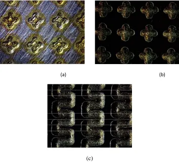
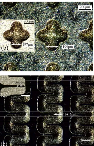
Figure 6. Comparison of the microstructures machined on nickel surfaces with those of a stainless-steel mould: (a) and (c) the nickel surface and, (b) and (d) the stainless stainless-steel mould. The machining parameters are a pulse-to-pause ratio of 1:3, a pulse width of 1 ms, a pulse amplitude of 6 V versus SCE and an etching time of 40 min.
Based on the above analysis, the optimized machining parameters are a pulse-to-pause ratio of 1:3, a pulse width of 1 ms, a pulse amplitude of 6 V versus SCE and an etching time of 40 min. To ensure the nickel electrode is in the transpassivation region instead of the passivation region, we set the pulse amplitude to 6 V versus SCE. The duration of the pulse is short enough to avoid the formation or aggregation of oxygen bubbles [14]. Thus, a short voltage pulse can significantly improve the quality of the electrochemical micromachining of the microstructures. Two complex microstructures were
[image:7.596.139.461.65.564.2]
successfully fabricated under the noted machining conditions, as shown in Fig. 6, showing that microstructure arrays with high uniformity were fabricated over a large area.
In Fig. 6(a) and 6(b), the average widths of the grooves on the stainless-steel mould and those of the fabricated workpiece are 199 µm and 197 µm, respectively. The deviation of the micromachined structure is nearly (199-197)/197×100% = 1.02%. Likewise, in Fig. 6(c) and 6(d) the deviation of the micromachined structure is nearly (198.2-196)/197×100% = 1.12%. These experimental results suggest that the microstructures were fabricated with high fidelity and accuracy.
4. CONCLUSIONS
In conclusion, uniform microstructure arrays have been fabricated on nickel surfaces by utilizing polyacrylamide gel as the template material and optimizing the process conditions, which proves that the electrochemical wet stamping technique is an easy, accurate, low-cost and green method for micromachining. The short voltage pulses applied in the experiment have high processing resolution and precision. The experimental results show that the machining deviations of the two fabricated microstructures are only 1.02% and 1.12%, respectively, of those of a stainless steel mould. Due to its simplicity and convenience, the E-WETS is particularly suitable for the rapid manufacture of various complex metallic three-dimensional microstructure arrays for applications in microelectronics, optics and microfluidics.
ACKNOWLEDGEMENTS
This work is supported by the National Natural Science Foundation of China under Grant No. 51605275.
References
1. B. Bhattacharyya, J. Munda, M. Malapati, Int. J. Mach. Tool Manu., 44 (2004) 1577-1589. 2. Z. Xiao, M. Dahmardeh, M. V. Moghaddam, A. Nojeh, K. Takahata, Microelectron. Eng., 150
(2016) 64–70.
3. W. L. Zhu, Z. Zhu, Y. He, K. F. Ehmann, B. F. Ju, S. Li, IEEE-ASME T. Mech., 22 (2017) 1796– 1806.
4. D. Zhu, N. S. Qu, H. S. Li, Y. B. Zeng, D. L. Li, S. Q. Qian, CIRP Ann-Manuf. Techn., 58 (2009) 177–180.
5. R. Schuster, V. V. Kirchner, P. Allongue, G. Ertl, Science, 289 (2000) 98–101. 6. M. Kock, V. Kirchner, R. Schuster, Electrochim. Acta, 48 (2003) 3213–3219.
7. Z. W. Tian, Z. D. Feng, Z. Q. Tian, X. D. Zhuo, J. Q. Mu, C. Z. Li, H. S. Lin, B. Ren, Z. X. Xie, W. L. Hu, Faraday Discuss, 94 (1992) 37–44.
8. L. J. Lai, H. Zhou, Y. J. Du, J. Zhang, J. C. Jia, L. M. Jiang, L. M. Zhu, Z. W. Tian, Z. Q. Tian, D. P. Zhan, Electrochem. Commun., 28 (2013) 135–138.
9. L. J. Lai, H. Zhou, Y. J. Du, C. X. Li, L. Zhang, L. M. Jiang, L. M. Zhu, Precis. Eng., 38 (2014) 569–577.
10.D. Landolt, P. F. Chauvy, O. Zinger, Electrochim. Acta, 48 (2003) 3185–3201.
11.L. Zhang, J. L. Zhuang, X. Z. Ma, J. Tang, Z. W. Tian, Electrochem. Commun., 9 (2007) 2529– 2533.
Electrochem. Commun., 33 (2013) 119–122.
13.H. Zhou, L. J. Lai, Y. J. Du, L. Zhang, L. M. Zhu, Electrochim. Acta, 111 (2013) 680–684. 14.J. Tang, L. Zhang, X. Tian, J. Micromech. Microeng., 20 (2010) 115030.
15.H. Zhou, L. J. Lai, X. H. Zhao, L. M. Zhu, Rev. Sci. Instrum., 85 (2014) 045122. 16.J. Scherer, B. M. Ocko, O. M. Magnussen, Electrochim. Acta, 48 (2003) 1169–1191.