Ian D. Flintoft
1, John F. Dawson
1, Linda Dawson
1, Andy C. Marvin
1, Jesus Alvarez
2and
Salvador G. Garcia
31Department of Electronics, University of York, Heslington, York YO10 5DD, UK 2Airbus Defence and Space, 28906 Getafe, Spain
3 Department of Electromagnetism and Matter Physics, University of Granada, 18071, Granada, Spain
Published in IEEE Transactions on Electromagnetic Compatibility, vol. 59, no. 1, pp. 111-118, 2017.
Accepted for publication: 31/07/2016
Early access on-line: 29/08/2016
DOI:
10.1109/TEMC.2016.2599004
Abstract— Computational solvers are increasingly used to solve complex electromagnetic compatibility problems in research, product design and manufacturing. The reliability of these simulation tools must be demonstrated in order to give confidence in their results. Standards prescribe a range of techniques for the validation, verification and calibration of computational electromagnetics solvers including external references based on measurement or for cross-validation with other models. We have developed a modular test suite based on an enclosure to provide the EMC community with a complex external reference for model validation. We show how the test suite can be used to validate a range of electromagnetic solvers. The emphasis of the test suite is on features of interest for electromagnetic compatibility applications, such as apertures and coupling to cables. We have fabricated a hardware implementation of many of the test cases and measured them in an anechoic chamber over the frequency range to 1 – 6 GHz to provide a measurement reference for validation over this range. The test-suite has already been used extensively in two major aeronautical research programmes and is openly available for use and future development by the community.
Index Terms— computational electromagnetics, validation, verification, benchmark problems
I. INTRODUCTION
o enable the use of computational electromagnetics (CEM) for both research and certification purposes it is necessary to prove the reliability of the computational modeling at producing realistic results. For this it is necessary to apply a systematic Validation, Verification and Calibration (VV&C) process to the development and deployment of CEM tools. A detailed explanation of the different aspects of
Submitted for review 28th March 2016. The research leading to these results has received funding from the UK Engineering and Physical Sciences Research Council (EPSRC) under the Flapless Air Vehicle Integrated Industrial Research (FLAVIIR) programme, grant GR/S71552/01, and from the European Community’s Seventh Framework Programme, FP7/2007-2013, under grant agreement number. 205294 on the High Intensity Radio-frequency Field Synthetic Environment (HIRF SE) research project.
I. D. Flintoft, J. F. Dawson, L. Dawson and A. C. Marvin are with The Department of Electronics, University of York, Heslington, York, UK (e-mail: [email protected], [email protected], [email protected], [email protected]).
J. Alvarez is with Airbus Defence and Space, 28906 Getafe, Spain (e-mail: [email protected]).
S. G. Garcia is with the Department of Electromagnetism and Matter Physics, University of Granada, 18071, Granada, Spain (email: [email protected]).
VV&C in the context of CEM and electromagnetic compatibility (EMC) is provided in [1]. In brief the three keys terms can be defined by [2], [3]:
Validation: “The process of determining the degree to which a model is an accurate representation of the real world from the perspective of the intended uses of the model”.
Verification: “The process of determining that a model implementation accurately represents the developer’s conceptual description of the model and the solution to the model”.
Calibration: “The process of adjusting numerical or physical modeling parameters in the computational model for the purpose of improving agreement with experimental data”. VV&C relies in part on the application of well defined canonical or benchmark reference problems [4]. Often these reference cases are based on exact analytical results for very simple geometries, though measurement references can also be used. Example reference models suitable for VV&C of CEM tools can be found in [4], [5]. Such reference cases can also be used for cross-validation between different CEM solvers, which is particularly salient to more complex reference problems for which analytic solutions are not available. Indeed, it is for the VV&C of complex structures that involve the interaction of many different sub-models within an overall simulation where there is a need for more systematic reference cases backed by reliable measurement.
In this paper we describe a modular test-suite of intermediate complexity that has been used extensively within two major research projects for the validation of computational electromagnetics (CEM) codes, with an emphasis on electromagnetic compatibility (EMC) applications. The test suite geometry is designed to cover a wide range of frequencies and operating modes, from quasi-static to reverberant. It allows comparison of the different features and the capabilities of various solvers to describe these features, for example apertures, materials and wires. A hardware implementation of the test object has been fabricated along with all of the modular components to allow measurement validation data to be obtained.
The test-suite is based on a hardware object that was originally constructed for validation of a hybrid finite-difference time-domain/finite element (FDTD/FEM) solver for aerospace simulations [6], [7]. The geometry was used again
A Modular Test Suite for the Validation and
Verification of Electromagnetic Solvers in
Electromagnetic Compatibility Applications
Ian D. Flintoft,
Senior Member, IEEE
, John F. Dawson,
Member, IEEE
, Linda Dawson,
Andy C. Marvin,
Fellow, IEEE
, J. Alvarez,
Member, IEEE
and Salvador G. Garcia,
Member, IEEE
aircraft against High Intensity Radio-Frequency (HIRF) threats [8][9]. Further development work continues for application in high frequency shielding simulations [10].
The rationale for the test suite was to construct a rigorously controlled and characterized generic object that incorporated features of interest to the EMC community, such as:
1. Coupling through apertures and joints; 2. Coupling to transmission lines; 3. Low loss, high Q-factor enclosures;
4. Absorption of radio-frequency energy by absorbing materials.
These features were designed in a modular fashion, allowing for the validation of single elements (for example an aperture model) or a combination of elements. It was also an objective to construct a hardware implementation of the test object that was suitable for accurate measurements up to 6 GHz. The final outcome was a test object consisting of a metallic box with a number of tests ports and an interchangeable panel that could contain apertures and joints and a selection of internal components such as wires and absorbers. It also includes a number of elements which act as transmission lines with varying levels of complexity (single straight wire, curved wire and a multiple conductor, straight transmission line).
The test suite is described in detail in Section II. The measurements used to characterize the probe antennas and a selection of the test cases are presented in Section III. In Section IV summary results of simulations of a small subset of the tests-cases in the frequency range 1-6 GHz using a range of solvers of different solver types are presented and compared using Feature Selective Validation (FSV), taking measurement data as a reference. We conclude in Section V.
II. TEST-OBJECT DESCRIPTION
A. The Enclosure
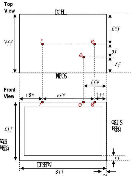
The test object is based on a physical brass box of (internal) dimensions 600 mm 500 mm 300 mm with a removable “front” face. The thickness of the walls is 1 mm to ensure that all energy penetration is due to the apertures. The physical geometry of the box is shown in Fig. 1. The front face can be left open or covered with a plate with different characteristics. The open face has a 30 mm wide flange around the edge with holes spaced at 26 mm (sides) and 28 mm (top and bottom) for fixing the interchangeable covering plates using 60 stainless steel captive bolts that protrude outwards. The box has three N-type connectors on the top, labeled A, B and C in the figure. Probe antennas or wire structures can be connected to these three ports. Additionally, absorbing material or other structures can be placed in the volume of the enclosure. A photograph of the enclosure is shown in Fig. 2.
The lowest cavity mode resonance in the empty enclosure, with the front face closed, is at 390 MHz. At 1 GHz there is a
total of 44 propagating modes and by 2 GHz this rises to around 300. The mode density at 2 GHz is 0.48 MHz-1 rising to 3.2 MHz-1 at 6 GHz. As a reverberation chamber the lowest usable frequency of the enclosure is approximately 1.5 GHz [11]. The frequency range therefore includes the physically interesting intermediate frequency range in which full-wave solvers begin to require prohibitive computational resources when applied to large objects such as complete aircraft and asymptotic solvers are still of limited validity.
B. Monopole probes
[image:3.612.331.553.53.349.2]Monopole probes can be attached to ports A, B or C. The physical probes are constructed using 50 N-Type bulkhead connectors and 3 mm diameter brass rod. The overall length of the monopoles from the internal side of the wall to the tip is 22 mm.
Fig. 1. Physical dimensions (in millimeters) of the test-object. enclosure.
Fig. 2. Photograph of the physical test-object enclosure. front
70 250
180
500 A B
C
A C B
100 335
165
300
30
30 600
left side
right side Front
View
bottom
[image:3.612.316.559.361.507.2]C. Wires and looms
A straight wire made from 3.5 mm diameter brass rod can be soldered to the ends of two probe antennas attached to ports A and B, thus forming a uniform transmission line of height 22 mm and length 335 mm. In addition, a curved wire has been fabricated, as shown in Fig. 3. This can also be soldered to the probes in the same ports. A more complex but well defined loom consisting of six 1 mm diameter wires arranged in a hexagonal cross-section has also been defined in the full test-suite [16].
D. Apertures, grills and joints
The enclosure can be used with an open face or a completely closed face. The physical implementation of the test-object with a fully closed face has been measured to have an isolation factor between the inside and outside of more than 90 dB up to 6 GHz. It is ultimately limited by the clamping pressure of the machine screws used to hold it in place and the surface finish of the brass plates. Care must be taken to ensure that the clamping pressure is consistent, particularly when the apertures in the face are not significantly larger than the spacing between the screws. Above 6 GHz the separation of the fasteners is less than half a wavelength and the isolation degrades.
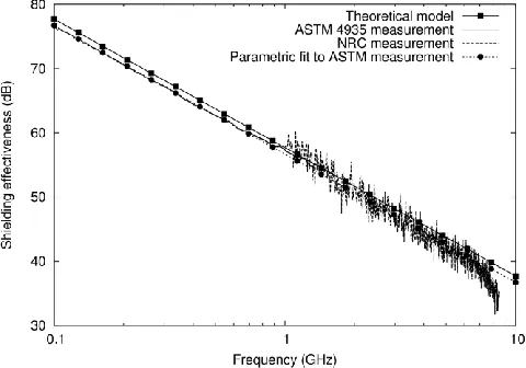
Further possibilities for the covering plate include aperture and joints structures. Fig. 4 shows the physical implementation of a perforated plate consisting of an array of 3 mm diameter circular holes arranged on a 21-by-21 square grid with a pitch of 10 mm. The plate thickness is 0.3 mm and the hole array is centered on the panel face. Regarded as an infinite array the shielding effectiveness of the array exhibits a 20 dB/decade increase with frequency until approximately 7 GHz where the electrical size of the holes and the spacing is approximately one tenth of a wavelength.
An approximate theoretical prediction for the normal
plane-wave incidence SE of a infinite plate uniformly perforated with circular holes of radius 𝑎 and pitch is given by
𝑆𝐸 (dB) = 20 log10 3c0Δ
2
16𝜋𝑎3
− 20 log10𝑓(MHz) − 32
𝑡
2𝑎− 120
(1)
where t is the plate thickness [12] and c0 is the speed of light in free space. This prediction is based on Bethe’s small apertures polarizability theory and neglects the mutual coupling between the apertures. The last term is added phenomenologically to account for the attenuation due to the cut-off waveguide effect of the sample thickness. For the above plate dimensions the contribution of the finite thickness term is 3.2 dB.
The physical implementation of the perforated plate was measured in an ASTM4935 coaxial cell [13] and nested reverberation chambers (NRCs) [14] and the results are shown in Fig. 5 compared to the theoretical model. The measurement using the nested reverberation chambers exhibits a statistical variation of about 4 dB due to the limited number of independent samples (32) taken in the measurement. A parametric fit to the measurement data gives
𝑆𝐸(dB) = 116.7 − 20 log10𝑓 (MHz) , (2)
which is within 1 dB of the above model. A two-sided surface impedance boundary condition (SIBC) corresponding to a shunt inductance of 42 pH provides a good model of the perforated plate over the frequency range 1 MHz to 6 GHz [15]. Other similar perforated plates have also been defined for use with the test object including anisotropic cases with rectangular slots at various angles with respect to the plate axes [16].
Front panels with larger apertures have also been defined and constructed. Fig. 6 shows a generic panel with two large apertures. The square aperture has a side length of 180 mm and the circular aperture a diameter of 100 mm. The physical implementation uses a 0.3 mm thick brass plate. These large apertures are useful for reducing the quality factor of the enclosure and increasing the energy coupled into the enclosure if dynamic range is an issue.
5 6 m m 5 6 m m
5 6 m m 7 5 m m
3 . 6 m m
[image:4.612.315.555.42.210.2]B o x W a ll
Fig. 3. Geometry of the curved wire that can be attached between port-A and port-B.
200mm
[image:4.612.51.277.63.137.2]200mm
Fig. 4. Physical implementation of the perforated plate front panel consisting of an array of circular holes arranged in a square grid.
[image:4.612.48.297.170.289.2]E. Internal absorbers
The enclosure is a high quality factor environment. Even with the front face left completely open there exist “end-to-end” modes with Q-factors in the low thousands over the frequency range 1 to 6 GHz. It is therefore often necessary or useful to damp the resonant behavior by introducing an absorber into the enclosure. The absorbing object itself can also be used to validate material models in computational tools.
The simplest absorbing element is a cubic piece of radio absorbing material (RAM) with a side length of 110 mm. The physical implementation was constructed from a number of layers of commercially available Eccosorb LS22 Series RAM sheet. The material is characterized by the manufacturer from 500 MHz to 18 GHz using the real and imaginary parts of the complex relative permittivity [17]. These material parameters have been fitted to a third order Debye relaxation model,
𝜀r(𝑠) = 𝜀∞+ ∑ ∆𝜀𝑖
1 + 𝑠𝜏𝑖 3
𝑖=1 , (3)
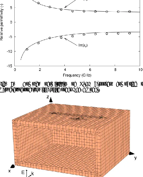
using a vector fitting algorithm [18]. Here we require that 𝜀∞≥ 1 for stability for the model. The parameters of the Debye model are given in Table I, where in this case we have enforced 𝜀∞= 1. The Debye model and manufacturers data are compared in Fig. 7.
The fit is accurate within the expected experimental uncertainty in the manufacturer’s measurement data and production tolerances over the frequency range 1 to 6 GHz. Better fits can be obtained by allowing 𝜀∞ to vary or by including an ionic conductivity term, −𝜎i⁄𝑗𝜔𝜀0, in the model, however, such models are not widely supported in computational solvers.
F. Source parameters and observables
Two types of excitation have been defined for the test configurations: port excitation and external plane wave illumination. For port excitation a matched source is used to inject power into port-A, which is connected to either a probe or wire. Such excitations are useful for detailed and accurate analysis of the behavior of the internal fields and surfaces currents.
For EMC immunity assessment external illumination is of interest and so two plane wave sources are defined. Firstly a unit plane wave source consisting of a single monochromatic, linearly polarized plane wave of amplitude 1 V/m illuminating the front face of the box as shown in Fig. 8. Both vertical (z -direction) and horizontal (y-direction) polarizations of the electric field are considered. A multiple plane wave source was also defined to take into account several plane waves illuminating the enclosure in order to validate the computation of short-circuited electromagnetic fields on apertures by asymptotic codes or full-wave codes for simulation scenarios of numerical coupling between external and internal solvers.
[image:5.612.313.555.66.235.2]Three types of observable are defined for the test-cases: Fig. 6. Generic front plate with two large apertures. All dimensions are in
millimeters.
80
100 100
60
60 60
180
Fig. 7. Complex permittivity of LS22 absorber, comparing the manufacturer’s data with a third order Debye model.
Fig. 8. Orientation of the unit plane wave excitation with vertical polarization (lower left) depicted on a computational mesh of the enclosure with an open face (CONCEPT-II mesh [20]).
TABLEI
DEBYE PARAMETERS OF LS22RAM DETERMINED FROM A VECTOR FIT TO THE MANUFACTURER’S COMPLEX PERMITTIVITY DATA (∞=1).
Parameter i = 1 i = 2 i = 3
i (-) 3.31 4.43 25.1
[image:5.612.315.555.106.403.2] [image:5.612.49.291.268.310.2]1. Power in a 50 load connected to a port. 2. Power density inside the cavity.
3. Electric field strength at the centers of apertures. In this paper we only consider the first of these; the power received in a load connected to one of the probes, Prec. For internal port sources the observables are usually presented as scattering parameters between the ports while for external illumination the received power is typically normalized to the incident power density at the front face of the enclosure, Sinc, to give a reception aperture
𝐴rec= Prec⁄𝑆inc . (4)
III. MEASUREMENT OF HARDWARE CONFIGURATIONS
A. Probe characterization
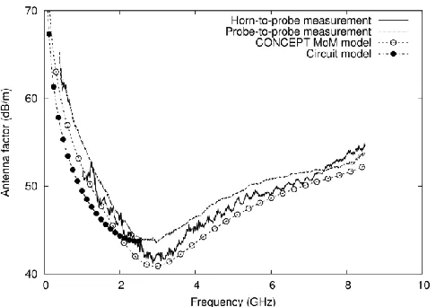
The hardware monopole probes have been calibrated by determining their free-space antenna factor (AF). This also allows the electric field strength from a simulation to be compared directly to the measurement data without the use of a wire model for the probe. This calibration was carried out using one-antenna and two-antenna methods [19], supported by MoM simulations and a circuit model. The results are shown in Fig. 9.
For the two-antenna method a reference ridged-waveguide horn antenna was used to measure the AF of each probe over a ground plane in the frequency range 1-8.5 GHz, the lower limit been determined by the working range of the horn. This showed that the two probes were almost identical in terms of their AFs (less than 0.2 dB difference); therefore only one of these measurement results is shown in Fig. 9. This measurement configuration is however subject to uncertainty due to diffraction effects when trying to launch a uniform plane-wave above the ground plane. A one-antenna method was therefore also applied over the band 200 MHz-8.6 GHz,
measuring the transmission between the two probes placed a known distance apart over an extended ground plane located in an anechoic environment. The fields in this configuration are subject to less uncertainty; the corresponding AF in Fig. 9 is typically a few decibels higher than the horn measurement.
The figure also shows the results of a method-of-moment (MoM) simulation of a probe above an infinite ideal ground-plane [20] and a simple circuit model of the monopole [21]. The MoM simulation used a thin-wire model of the monopole, which will introduce an error due to the relatively large diameter of the monopoles. The simple circuit model stops at 2 GHz as this model is only valid to just beyond the first resonance of the monopoles. These results indicated the typical uncertainty that may be encountered when comparing measurement and simulation made under different assumptions and approximations.
To determine the phase delay between the reference plane of the probe connector and the base of the monopole the probe was shorted to the ground plane using metal foil and the complex reflection coefficient was measured relative to the reference plane. Calibration of this phase delay is important when comparing the measurement results to simulation data at high frequencies.
B. Anechoic chamber measurements
[image:6.612.314.562.40.208.2]Most of the measurements on hardware configurations took place in an anechoic chamber over a frequency range of 1 to 6 GHz using a vector network analyzer (VNA) with cable effects and phase delay of antennas calibrated out. Fig. 10 is a photograph of the enclosure with the front panel with two large apertures in place being tested in an anechoic room. The enclosure was illuminated by a horn antenna located near the camera position to generate a plane wave source condition. The power received at port-A is being monitored by the blue test cable while the other port is terminated. To calibrate the incident power density the enclosure was removed and another co-polar horn placed with its phase center at the location of the front face.
Fig. 10. Test-case with generic front plate on-test in an anechoic chamber.
[image:6.612.48.291.55.226.2]of the test-cases implemented using a range of solvers. The implementations were made directly from the written test-case specification, so for example, no CAD or meshes were shared between the different implementations. The results therefore intentionally reflect the variability associated with interpretation of the specification and detailed choice of modeling technique applied. We have used FSV [4] and Integrated Error Logarithmic Frequency (IELF) [22] algorithms to compare the results from the different solvers using the measurement data as a reference. The rationale is to demonstrate the variability in the results that can be expected from the implementation of a complex test-case for which analytic results are not available and choices concerning the representation of different features in the specification in a particular solver have to be made. We do not directly compare solvers (which are anonymized) with respect to their accuracy or capability, though some observations about different types of solver are made.
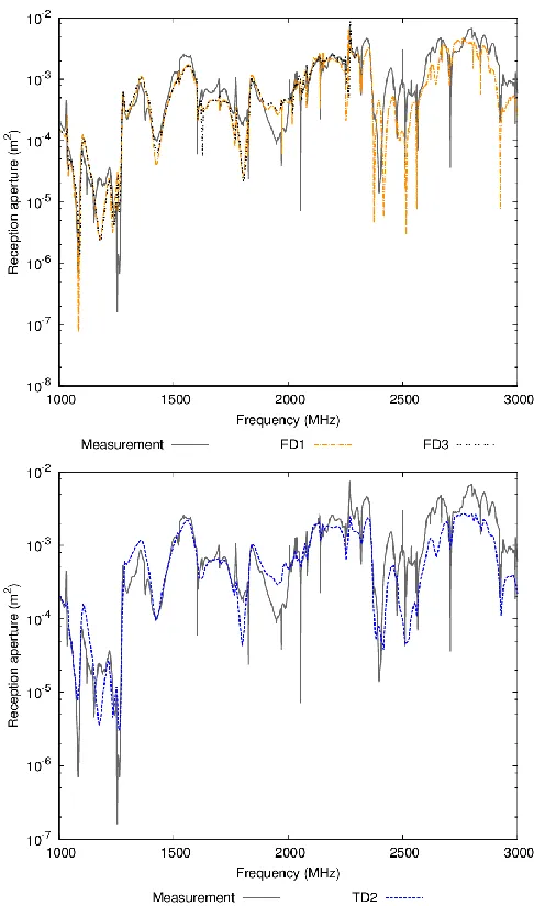
A. Test-case 1
The configuration of test case 1 consists of the enclosure with an open face and two terminated probe antennas on ports A and B. The enclosure is illuminated by a plane wave and the power received at port A is observed. The results for two frequency-domain and one time-domain solver are shown in the top and bottom parts of Fig. 11 respectively. Table II shows the FSV amplitude difference measure (ADM) and feature difference measure (FDM) for each pair of results. The FSV global difference measure (GDM) and IELF values are shown in Table III.
Even for this simplest test-case in the test-suite the FSV qualitative GDM is no better than ‘fair’. IELF and the FSV GDM give consistent rankings of the data comparisons. There is no strong indication that the measurement data proves a worse reference than the solvers as a base for cross-comparisons. Overall the results seem reasonable for “one-shot” simulations with no iterative refinement of the models.
B. Test-case 2
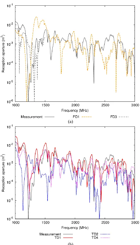
Introducing the cube of LS22 RAM into the centre of the lower surface of the enclosure and the curved wire (as shown in Fig.3) between ports A and B gives test case 2. The reception aperture, defined in (4), measured at port-A for this test-case is shown in Fig. 12 for two frequency-domain and three time-domain solvers. The FSV and IELF metrics are given in Table IV and Table V.
For this more complex test case the FSV GDM is generally “poor” or “very poor” with the dominant contribution coming from the ADM. The rankings provided by IELF and FSV GDM are broadly consistent but not identical, particularly with regard to the datasets with poorer metrics. Here there is some evidence that the measurement data provides a reference with the lowest overall metrics across all the datasets.
The measurement uncertainty itself is estimated to be no more than about 1 dB for most of the test-cases and we expect
that the leading cause of the deviations is the “modeling error” introduced by the simplifications of the real physical geometry made in the simulations. The test-case is dependent on many Fig. 11. Reception aperture for test case 1 from 1-3 GHz comparing frequency-domain codes (top) and time–domain codes (bottom) to measurement.
TABLEII
FSVADM(ABOVE DIAGONAL) AND FDM(BELOW DIAGONAL) FOR TEST CASE 1.FIGURES IN BOLD CORRESPOND TO QUANTITATIVE FSV VALUES LESS THEN UNITY.
Measurement FD1 FD3 TD2
Measurement - 0.38 0.33 0.82
FD1 0.56 - 0.20 0.53
FD3 0.38 0.32 - 0.49
TD2 0.62 0.45 0.46 -
TABLEIII
FSVGDM(ABOVE DIAGONAL) AND IELF METRIC (BELOW DIAGONAL) FOR TEST CASE 1.FIGURES IN BOLD CORRESPOND TO QUANTITATIVE FSV VALUES LESS THEN UNITY.
Measurement FD1 FD3 TD2
Measurement - 0.75 0.56 1.10
FD1 0.72 - 0.42 0.75
FD3 0.56 0.21 - 0.74
[image:7.612.314.557.58.470.2]aspects of the numerical modeling of the real system including dispersive material properties the treatment of thick wires. The larger spread in the FSV and IELF metrics reflects this increased complexity and highlights the need for iterative calibration of simulation tools against more realistic test-cases with multiple features.
Our purpose here was to introduce and demonstrate the test-suite; in a real-world situation further calibration of the models would be necessary if the measurement reference is assumed to be authoritative. The first step in a calibration process would be to identify dominant “modeling errors”, for example by a sensitivity analysis of the models, and then to refine the simulations accordingly until the deviation between model and measurements is comparable to the measurement uncertainty.
V. CONCLUSIONS
An extensive modular test-suite for use in VV&C of CEM solvers for EMC applications has been developed. The test
cases, while still relatively simple compared to real systems, are of a greater complexity than many of the generic canonical references currently available allowing interactions between different modeling aspects to be evaluated using a well-defined set of geometries. Hardware implementations of many of the possible test configurations have been constructed and measured to provide a database of reference data.
The test configurations have been widely used for cross validation between different types of solvers within a number of large research programmes. We have demonstrated the use of the test-suite by presenting summary results for a range of solvers applied to small sub-set of test-cases using the measurement data as a reference. FSV and IELF comparisons of the results highlight the difficulties inherent in the VV&C process for systems of even modest complexity and the importance of calibration to attaining reliable results.
The measurement data-sets, CAD files for some of the geometries and extensions to the test case are freely available for use [16].
ACKNOWLEDGMENT
We gratefully acknowledge the many contributions, in the form of corrections, clarifications of the geometries and ideas for extensions, provided by members of the HIRF-SE consortium including Jean-Philippe Parmantier of The Office National d'Etudes et de Recherches Aérospatiales (ONERA), Marco Kunze of Computer Simulation Technology (CST) AG and John Kazik of Ingegneria dei Sistemi UK (IDS-UK).
We also thank The University of Nottingham (Chris Smartt), QWED Sp.z.o.o. (Janusz Rudnicki), BAE Systems Ltd (Chris Jones and Geoff South), The Technische Universität Hamburg-Harburg (Heinz Brüns) for providing the simulations results presented in Section IV of the paper.
REFERENCES
[1] L. Sevgi, “Electromagnetic modeling and simulation: Challenges in validation, verification and calibration”, IEEE Transactions on
Electromagnetic Compatibility, vol. 56, no. 4, pp. 750-758, Aug. 2014.
TABLEIV
FSVADM(ABOVE DIAGONAL) AND FDM(BELOW DIAGONAL) FOR TEST CASE 2.FIGURES IN BOLD CORRESPOND TO QUANTITATIVE FSV VALUES LESS THEN UNITY.
Measurement FD1 FD3 TD1 TD2 TD4
Measurement - 1.36 1.30 0.68 1.90 0.48
FD1 0.63 - 4.0 0.75 6.4 1.9
FD3 0.62 0.50 - 2.9 0.99 1.0
TD1 0.51 0.57 0.88 - 3.7 1.1
TD2 0.80 1.00 0.46 1.10 - 1.4
TD4 0.32 0.65 0.56 0.61 0.75 -
TABLEV
FSVGDM(ABOVE DIAGONAL) AND IELF METRIC (BELOW DIAGONAL) FOR TEST CASE 2.FIGURES IN BOLD CORRESPOND TO QUANTITATIVE FSV VALUES LESS THEN UNITY.
Measurement FD1 FD3 TD1 TD2 TD4
Measurement - 1.6 1.5 0.92 2.2 0.63
FD1 1.4 - 4.2 1.0 6.6 2.1
FD3 1.7 2.5 - 3.2 1.2 1.3
TD1 0.94 1.1 1.5 - 4.0 1.4
TD2 1.8 2.1 1.6 1.9 - 1.7
TD4 0.95 1.2 1.1 1.0 1.5 -
(a)
(b)
[image:8.612.49.295.46.477.2](AIAA), Report AIAA G-077-1998, 1998.
[3] Oberkampf, T. Trucano and C. Hirsch, “Verification, validation and predictive capability in computational engineering and physics”, Appl.
Mech. Rev., vol. 57, no. 5, pp. 345-384, 2004.
[4] IEEE STD 1597.1, “IEEE Standard for validation of computational electromagnetics computer modeling and simulations”, IEEE, NY, IEEE, 2008.
[5] IEEE STD P1597.2, “Recommended practice for validation of computational electromagnetics computer modeling and simulations”, IEEE, NY, 2010.
[6] J. F. Dawson, C. J. Smartt, I. D. Flintoft, C. Christopoulos, “Validating a numerical electromagnetic solver in a reverberant environment,” IET 7th International Conference on Computation in Electromagnetics
(CEM2008), Brighton, UK, pp. 42-43, 7-10 April, 2008.
[7] C. Christopoulos, J. F. Dawson, L. Dawson, I. D. Flintoft, O. Hassan, A. C. Marvin, K. Morgan, P. Sewell, C. J. Smartt and Z. Q. Xie, “Characterisation and Modelling of Electromagnetic Interactions in Aircraft”, Proceedings of the Institution of Mechanical Engineers, Part
G: Journal of Aerospace Engineering: Special Issue on FLAVIIR, Vol.
224, No. 4, 2010, pp. 449-458.
[8] D. Tallini, J. F. Dawson, I. D. Flintoft, M. Kunze and I. Munteanu, “Virtual HIRF Tests in CST STUDIO SUITE - A Reverberant Environment Application”, International Conference on Electromagnetics in Advanced Applications (ICEAA2011), Special
Session on Numerical Methods for Challenging Multi-Scale Problems,
Torino, Italy, 12-16 September, 2011. pp. 849-852.
[9] J. Alvarez, L. D. Angulo, A. R. Bretones and S. G. Garcia, “A comparison of the FDTD and LFDG methods for the estimation of HIRF transfer functions”, Computational Electromagnetics for EMC
(CEMEMC’13), Granada, Spain, 19-21 March 2013.
[10] A. C. Marvin, I. D. Flintoft, J. F. Dawson, M. P. Robinson, S. J. Bale, S. L. Parker, M. Ye, C. Wan and M. Zhang, “Enclosure shielding assessment using surrogate contents fabricated from radio absorbing material”, 7th Asia-Pacific International Symposium on Electromagnetic Compatibility & Signal Integrity and Technical Exhibition (APEMC 2016, Shenzhen, China, 18-21May, 2016.
[11] IEC, “Electromagnetic compatibility (EMC) - Part 4-21: Testing and measurement techniques - Reverberation chamber test methods”, International Electrotechnical Commission, standard 61000-4-21, 2nd edition, January, 2011.
[12] K. F. Casey, “Electromagnetic shielding behavior of wire-mesh screens”, IEEE Transactions on Electromagnetic Compatibility, vol.30, no.3, pp.298-306, Aug. 1988.
[13] STM Standard D4935-10, “Standard test method for measuring the electromagnetic shielding effectiveness of planar materials”, ASTM International, West Conshohocken, PA, June, 2010.
[14] C. L. Holloway, D. A. Hill, J. Ladbury, G. Koepke and R. Garzia, “Shielding effectiveness measurements of materials using nested reverberation chambers” IEEE Transactions on Electromagnetic
Compatibility, vol.45, no.2, pp. 350- 356, May 2003.
[15] I. D. Flintoft, J. F. Dawson, A. C. Marvin and S. J. Porter, “Development of Time-Domain Surface Macro-Models from Material Measurements”, 23rd International Review of Progress in Applied
Computational Electromagnetics (ACES2007), Verona, Italy, 19-23
March, 2007.
[16] AEG Box Test Suite, URL: https://bitbucket.org/uoyaeg/aegboxts. [17] Emerson and Cuming Microwave Products, ECCOSORB LS Material
Data Sheet. [Online]. Available: http://www.eccosorb.com.
[18] B. Gustavsen and A. Semlyen, “Rational approximation of frequency domain responses by vector fitting”, IEEE Transactions on Power
Delivery, vol. 14, pp. 1052 -1061, 1999.
[19] C. A. Balanis, Antenna Theory: Analysis and Design, 3rd edition, John Wiley, NJ, 3 May 2005.
[20] Technische Universität Hamburg-Harburg. The CONCEPT-II website (2016). [Online]. Available: http://www.tet.tuhh.de/concept
[21] T. G. Tang, Q. M. Tieng and M. W. Gunn, “Equivalent circuit of a dipole antenna using frequency independent lumped elements”, IEEE
Transactions on Antennas and Propagation, vol. 41, no. 1, pp. 100-103,
1993.