Journal of Materials Chemistry C
ARTICLE
Please do not adjust margins
a.WestCHEM, Department of Pure and Applied Chemistry, University of Strathclyde,
Glasgow, G1 1XL, UK. E-mail: [email protected]
b.Lviv Polytechnic National University, S. Bandera 12, 79013 Lviv, Ukraine. c.Institute of Materials Science, Kaunas University of Technology, Baršausko str. 59,
LT-51423 Kaunas, Lithuania.
d.Department of Polymer Chemistry and Technology, Kaunas University of
Technology, Radvilenu Plentas 19, LT-50254 Kaunas, Lithuania.
† Footnotes relating to the title and/or authors should appear here.
Electronic Supplementary Information (ESI) available: [experimental procedures, cyclic voltammetry, spectroscopy data, AFM, modelling, TGA]. See DOI: 10.1039/x0xx00000x
Received 00th January 20xx, Accepted 00th January 20xx
DOI: 10.1039/x0xx00000x
www.rsc.org/
A single emitting layer white OLED based on exciplex interface
emission
E. Angioni,a M. Chapran,b K. Ivaniuk,b N. Kostiv,b V. Cherpak,b P. Stakhira,b,* A. Lazauskas,c S. Tamulevičius,c D. Volyniuk,d N. J. Findlay,a T. Tuttle,a J. V. Grazuleviciusd,* and P. J. Skabaraa,*
A new triaryl molecule based on a benzene-benzothiadiazole-benzene core has been applied in a WOLED device. This very simple molecule emits from a combination of emissive states (exciton/electromer/exciplex/electroplex) to give white light with CIE coordinates of (0.38, 0.45) and a colour temperature of 4500K.
Introduction
During the last two decades, the swift development of new and high performing inorganic and organic emissive materials has brought to the market competitive and efficient solid state lighting (SSL) devices. They are predicted to become the next generation of general illumination systems.1 Inorganic white
light emitting diodes (LEDs) are commercially used nowadays for general illumination purposes (e.g. automotive lighting, indoor and outdoor lighting).2 White organic light emitting
diodes (WOLEDs) instead are principally used as low-cost alternatives for back-lights in flat panel displays.3 They present
several advantages compared to their inorganic counterparts, such as lower cost, ease of processability and facile tuning of their properties by chemical modifications.3, 4 Furthermore,
they can be fabricated as flexible panels with wide viewing angles and a superior white colour balance.5 White SSL can be
achieved using different approaches, but commercially successful methods include: (I) combining a blue (ca. 460 nm) LED and a yellow phosphor pumped from the blue light of the LED;6-8 (II)combining a single chip emitting UV light which is
absorbed in the LED package by three phosphors (red, green and blue) and re-emitted as a broad spectrum of white light9, 10
or (III) three different LED chips, each emitting a different wavelength [red, green and blue (RGB)] in order to simulate the RGB colour model.9-15 The design of these configurations is
not straightforward and to achieve competitive efficiencies
and luminosity the use of hybrid (inorganic-organic) solutions has been explored.11-13, 16 Furthermore, white light produced in
this fashion is difficult to fine-tune, in particular when a mixture of several emitters is used.17 In order to simplify the
device architecture, several strategies have been used to fabricate single molecular layer WOLEDs.5 Heagy et al.
employed N-aryl-2,3-naphthalimides with low symmetry that exhibited efficient panchromatic emission.18, 19 Liu et al.
observed white solid-state luminescence as well as electroluminescence from the controlled protonation of a molecular blue fluorophore,20 while Chou et al. showed
white-light emission in a single excited-state-intramolecular-proton-transfer (ESIPT) system by fine-tuning the energetics of the excited state.21 White-light emission can also be achieved from
intermolecular interactions or from the formation of complexes, e.g. excimers or exciplexes.17, 22-26 Excimers are
possible in single component organic materials due to the resonance interaction of a molecular exciton with a neighbour non-excited molecule,27-29 whereas exciplexes can be formed
in a bi- or multi-component molecular solid when the formation of bimolecular excited states is facilitated by electron transfer between the donor and acceptor components.30, 31 In 2002 Wang and co-workers reported a
highly efficient white device based on the exciplex between a boron complex and N,N′-di(1-naphthyl)-N,N′-diphenylbenzidine (NPB).32 Qiu and co-workers observed
exciplex type white-light emission from the interface of a bilayer electroluminescent device consisting of a new electron transport material, anthracene-9,10-diylbis(diphenyl-phosphine oxide) (DPPA) and N,N’-bis(naphthalen-1-yl)-N,N'-bis(phenyl)benzidine (NPB)22 as the hole-transporting layer.
ARTICLE Journal Name
2 | J. Name., 2012, 00, 1-3 This journal is © The Royal Society of Chemistry 20xx
Please do not adjust margins
Please do not adjust margins
FIrpic.26 In this work, an OLED based on the new compound
dimethyl 4,4'-(benzo[1,2,5]thiadiazole-4,7-diyl)bis(3-methoxybenzoate) (1) has been fabricated and its performance studied.
Results and discussion
Synthesis and opto-electronic properties
Compound 1 was synthesised from commercially available 4,7-
bis(4,4,5,5-tetramethyl-1,3,2-dioxa-borolan-2-yl)benzo[c][1,2,5]thiadiazole via Suzuki-Miyaura cross-coupling with methyl 4-iodo-3-methoxybenzoate33 (2) (Fig. 1a). In the
UV-Vis absorption spectrum of 1 (10−5 M in dichloromethane)
(Fig. 1b) the typical absorption band of the benzothiadiazole (BT) core34-36 is blue shifted to 295 nm (19300 M−1 cm−1) and its
vibronic fine structure is visible. In a similar fashion, the less intense band, attributable to the interaction between the peripheral benzene rings and the core (HOMO-LUMO transition, Table S1, ESI) is blue shifted and centered at 366 nm (9500 M−1 cm−1). This is likely due to the non-planarity of 1,
contrary to some planar 4,7-di-substituted benzothiadiazole analogous compounds.36-38 From the longest wavelength
absorption edge of the UV-Vis absorption spectrum (Fig. 1) it was possible to calculate an optical HOMO-LUMO gap of 3.0 eV. Photoluminescence measurements were performed for
250 300 350 400 450 500 550 0.0 0.2 0.4 0.6 0.8 1.0 0.0 0.2 0.4 0.6 0.8 1.0
Norm. Absorption (a.u.)
Norm. Emission
(a.u.)
Wavelenght (nm)
b)
Fig. 1 (a) Synthesis of compound 1 (58% yield). (b) UV–Vis absorption spectrum (black)
of a solution of 1 in dichloromethane (10−5 M) and the emission spectrum of the solution of 1 in dichloromethane (blue) and tetrahydrofuran (10−6 M) at different temperatures (300K, green; 77K, red). The solutions were excited at 366 nm (dichloromethane) and at 330 nm (tetrahydrofuran).
a dilute dichloromethane solution of 1 (10−6 M) at 300K
(excitation at 366 nm) and for a dilute THF solution of 1 (10−6
M) at 300 and 77K (excitation at 330 nm) showing emission maxima at 472, 487 and 449 nm, respectively. Furthermore, photoluminescence quantum yields (PLQYs) of ca. 50% and ca. 6 % were recorded at 300K using an excitation wavelength of 366 nm for the dilute dichloromethane solution of 1 (10−6 M)
and for the encapsulated powder of 1 (pressed against two glass substrates), respectively. The red shift with decreasing polarity of solvent is likely due to the donor-acceptor character of 1. In the excited state one expects a large dipole moment due to charge transfer and thus a high sensitivity to solvent polarity. Instead, as the temperature of THF is decreased to 77K, the emission spectrum of 1 is observed from a less relaxed excited state resulted in a shift of the fluorescence maxima to shorter wavelengths.39-41
Cyclic voltammograms were recorded for a dilute solution of 1 in dichloromethane using tetrabutylammonium hexafluorophosphate as the supporting electrolyte. They show a reversible reduction (−1.99/−1.87 V) and three irreversible oxidations (1.36, 1.50, 1.63 V) (Fig. S1, ESI). The reduction process can be attributed to the semi-reversible reduction of the BT unit, known to be an electron acceptor,42 whereas the
anodic waves can be attributed to the oxidation processes likely localised on the methoxy groups as revealed in similar 4,7-bis-substituted BT compounds.43, 44 The electrochemical
HOMO and LUMO levels were calculated from the onset of the first oxidation wave (−6.0 eV), and reduction wave (−2.9 eV), respectively (the data were referenced to ferrocene, which has a HOMO of −4.8 eV).45 The electrochemical HOMO-LUMO gap
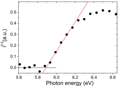
was therefore determined to be 3.1 eV. With respect to the HOMO energy determined by CV (−6.0 eV), a very close value of 5.9 eV was also calculated as the HOMO level from the photoelectron emission spectrum of the solid state film obtained by vacuum deposition onto an indium tin oxide (ITO) coated glass substrate (Fig. S2, ESI). The electrochemical HOMO and LUMO energies were used for the development of the device conception and in the following energy diagrams.41, 46
Morphology and charge transport properties
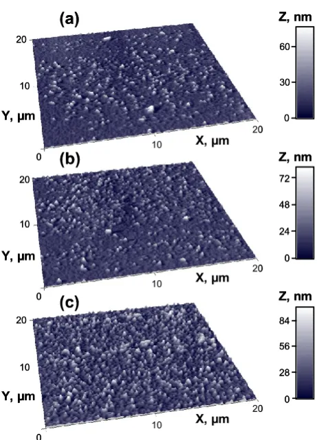
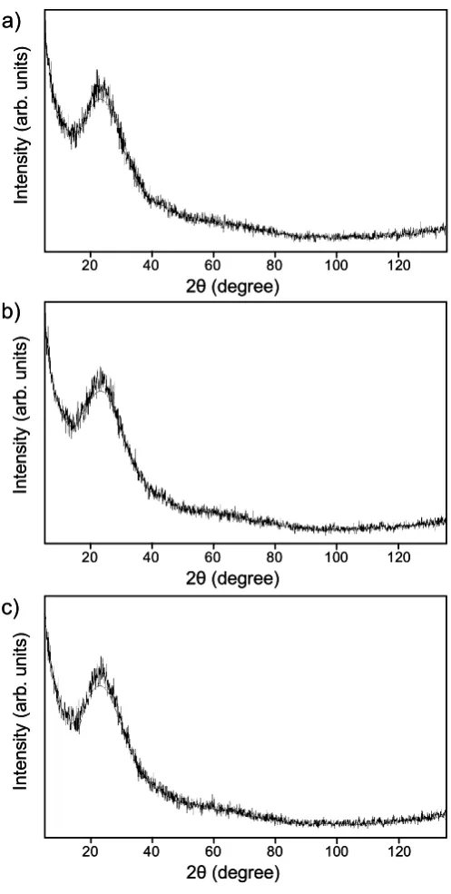
AFM measurements were performed on vacuum deposited layers of 1 at different deposition rates on glass substrates: (a) < 0.1Å s−1, (b) 1.5 Å s−1 and (c) 10 Å s−1 (Fig. S3, ESI). They show
random oriented pillar/needle-shaped surfaces with the mean height of the peaks (18.41 nm, 20.07 nm and 25.53 nm) and the root mean square roughness (9.38 nm, 10.62 nm and 15.99 nm) increasing with the deposition rate. The surfaces are dominated by peaks with a skewness (RSk) of 2.25, 1.63 and 1.29, respectively, and they have a leptokurtic distribution of the morphological features with a kurtosis (RKu) of 11.10, 7.58 and 5.20, respectively. The X-ray diffraction patterns recorded on the samples deposited at (a) < 0.1Å s−1, (b) 1.5 Å s−1 and (c)
10 Å s−1 (Fig. S4, ESI) show a completely amorphous structure
for 1, independent of the deposition rate.
[image:2.595.51.283.385.688.2]Journal Name ARTICLE
Please do not adjust margins
be used to measure the charge carrier mobility in thin films of low molar mass compounds.47 Hole-only and electron-only
devices were prepared using 4,4′,4′′-tris[3-methylphenyl(phenyl)amino]triphenylamine (m-MTDATA) as the hole-injecting/electron-blocking layer and 1,3,5-tris(N-phenylbenzimidazol-2-yl)benzene (TPBi) as the electron-injecting/hole-blocking layer. The two devices were fabricated by successive deposition onto a pre-cleaned indium tin oxide (ITO) coated glass substrate under a vacuum of 10−6 Torr, with
architectures of: ITO/m-MTDATA(20 nm)/1(60 nm)/m-MTDATA(20 nm)/Al(60 nm) (hole-only) and ITO/TPBi(20 nm)/1(60 nm)/TPBi (20 nm)/Ca(10 nm)/Al(60 nm) (electron only). The hole mobility of 1 (7.6 × 10⁻⁷ cm2 V−1 s−1 at 9.6 × 10⁵
V cm−1) has a higher value than the electron mobility (1.7 ×
10−7 cm2 V−1 s−1 at 9.6 × 10⁵ V cm−1; Fig. S5, ESI). The fitted
parameters μ0 and γ are 2.6 × 10⁻⁸ cm2 V−1 s−1 and 3.4 × 10⁻³ cm
V−1, and 2.8 × 10⁻⁹ cm2 V−1 s−1 and 4.2 × 10⁻³ cm V−1 for holes
and electrons, respectively (Fig. S6, ESI). Despite the low charge mobility, 1 can be used successfully for the preparation of emitting layers, due to the nano-scale thicknesses required for the OLED fabrication.48
Device fabrication and exciplex emission
An electroluminescent device based on 1 was fabricated. Due to the morphology, the low mobility and the energetically deep HOMO level of 1, N,N′-bis(3-methylphenyl)-N,N′-diphenylbenzidine (TPD) was used as hole-transporting material to promote a cross-interaction between the excess of electrons from the LUMO of 1 and the excess of holes from the HOMO of TPD with the aim of inducing the formation of a dimeric excited state (e.g. exciplex). 2,9-Dimethyl-4,7-diphenyl-1,10-phenanthroline (BCP) was used as an electron-transporting/hole-blocking layer in order to increase the injection of electrons from the calcium anode and to balance the amount of electrons and holes that combine in the emissive layer. Additionally, to promote hole and electron mobility, CuI was used as a hole-injecting material.
The electroluminescent device (Fig. S7, ESI) was fabricated by successive deposition onto a pre-cleaned indium tin oxide (ITO) coated glass substrate under a vacuum of 10−5 Torr using
specific deposition rates for the different layers: ITO/CuI (8 nm, 0.1 nm s−1)/TPD (10 nm, 0.2 nm s−1)/1 (100 nm, 1 nm
s−1)/BCP (30 nm, 0.2 nm s−1)/Ca (7 nm, 0.1 nm s−1)/Al (100 nm,
0.1 nm s−1). The active area of the obtained device was 6 mm2
and additional passivation was not applied. The fast deposition rate (10 Å s−1) was adopted in the device fabrication process in
order to facilitate the creation of an interaction with the adjacent layers. The electroluminescence (EL) spectrum of the device recorded with an applied voltage of 15 V (Fig. 2a) reveals four superimposed different emission bands. The origins of these bands are shown in Fig. S8. The higher energy emission band (494 nm) is characteristic of the pure fluorescence emission of 1. This is supported by the luminescence decay time measurements of the spin coated film of 1 (at 488 nm, ca. 10−2 M in THF) being on a nanosecond
scale (Fig. 2b) and from the single emission band centred at 490 nm in its photoluminescence spectrum (Fig. 2a).49 The
main band at ca. 580 nm originates from the exciplex at the interface between 1 and the hole-transporting material TPD. In fact, the luminescence decay time measurements (at 580 nm) of the composite layer prepared by spin coating a solution of 1 and TPD (ca. 0.01M in THF) onto a clean quartz substrate shows a combination of 17 ns (41%) and 61 ns (59%) decay times (Fig. 2b), due to the presence of both the exciton fluorescence emission and the exciplex emission at the interface between TPD and 1.26, 49, 50 When a direct bias is
applied, due to high energy barriers between TPD and 1 (HOMOTPD − HOMO1 = 0.5 eV; LUMOTPD − LUMO1 = 0.6 eV), electrons and holes accumulate at the interface between the two layers and, due to non-planar conformations, the electronic overlap of donor (TPD) and acceptor (1) molecules is efficient for exciplex formation at the interface. In fact, the twisted nature of 1 makes self-stacking less likely, increasing the probability of a hetero-interaction with an adjoining molecule. The long-wavelength shoulder at 635 nm in the EL spectra can be assigned to the typical (classic) electroplex interaction that is associated with the exciplex emission.49, 51
The band at ca. 520 nm can be attributed to an electromer interaction, that appears upon the injection of electrons and holes under an electric field effect in 1.52, 53 The formation of
an electromer is
400 500 600 700 800
0.0 0.2 0.4 0.6 0.8 1.0 0.0 0.2 0.4 0.6 0.8 1.0 Norm
. PL intens
ity
(a.u.)
Norm
. EL intens
ity (a.u.) Wavelength (nm) 8 V 10 V 12 V 14 V 15 V 16 V 17 V 1 TPD:1 a)
0 50 100 150 200 250 300
1 10 100
1000 b)
TPD:1 :
=17 ns (41%)
=61 ns (59%)
1.137
1 TPD:1 Fitting Counts Time (ns) 1:
=4.76 ns
1.117
Fig. 2 (a) Electroluminescence spectra of the OLED at selected applied voltages and
[image:3.595.308.546.361.719.2]ARTICLE Journal Name
4 | J. Name., 2012, 00, 1-3 This journal is © The Royal Society of Chemistry 20xx
Please do not adjust margins
Please do not adjust margins
w/w). (b) Decay fluorescence plots measured for the thin films of 1 (at 488 nm) and ofthe mixture of TPD with 1 (at 580 nm).
observed when a pair of trapped carriers recombines under an electronic interaction and its emission is red-shifted with respect to fluorescence.51 Therefore, the white emission of the
device originates from the combination of the exciplex/electroplex emission at the interface between TPD and 1 and from the exciton/electromer emission of 1. This is possibly due to the thickness of the emissive layer (100 nm) that permits emission from all the excited states simultaneously. The EL spectra at different applied voltages were recorded (Fig. 2a) and they reveal four different emission bands, with relative intensities that depend on the applied voltage. The maxima of the higher energy emission band (494 nm) and of the electromer emission (520 nm) stay constant with increasing applied voltage, whilst the relative intensities increase. The main emission maximum is blue-shifted from 588 to 570 nm when the applied voltage is increased from 8 to 17 V. Conversely, both the position and the intensity of the shoulder at 635 nm remains effectively unchanged at the different applied voltages. Despite these behaviours, the colour quality of the device is maintained at all applied voltages. The CIE coordinates change only slightly from (0.42, 0.44) when the EL is recorded at 8 V to (0.37, 0.44) at 17 V (Fig.
S9 and Table S2, ESI), due mainly to the increased relative
intensity of the EL and of the electromer transition of 1. However, at applied voltages higher than 15 V, the device tends to quickly degrade and the characteristics recorded are not maintained. For this reason the following characteristics of the device were recorded up to a maximum applied voltage of 15 V.
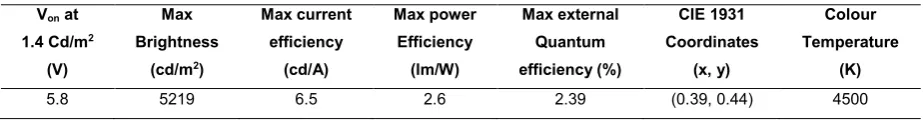
The current density−voltage characteristics and luminance−voltage characteristics (Table S3-S4, ESI) indicate an OLED turn on voltage of 5.8 V, which corresponds to an electroluminescence of 1.4 cd m−2. The device exhibits a
maximum current efficiency of 6.5 cd A−1 and a maximum
brightness of 5219 cd m−2 (at 15 V) (Fig. S10-S12, ESI). At
maximum brightness an external quantum efficiency of 2.39% and power efficiency of 2.60 Lm W−1 were recorded. The white
light emitted from the device at 15 V has Commission Internationale d’Eclairage (CIE 1931) coordinates of (0.38, 0.45) (Fig. S9), with a colour temperature of 4500K; values similar to those of commercial fluorescent tubes.13, 54, 55 The
relatively low brightness and current efficiency of the single-layer OLED can be explained by the presence of electroplex emission that naturally results in the decrease of OLED efficiency.56 On the other hand, the presence of the
electroplex-type excited states makes it possible to expand the EL spectrum towards the red region and to obtain a white OLED with a simplified structure.56
Computational results
To explain the PL and EL spectra observed experimentally, quantum chemical calculations were performed for 1, TPD and
1:TPD complexes using density functional theory (DFT) and its
time resolved counterpart (TD-DFT).57, 58 In order to choose the
most suitable level of theory capable of simulating the vertical transitions associated with the absorption spectra, a benchmark was performed (Table S5, ESI) and, as a result, the PBE0/6-311G(d,p) level of theory was used for all the calculations. Initially eight different geometric isomers of the
TPD:1 complexes (a-h) were optimised (Fig. S13, ESI), with
isomer a showing the total energy minima and hence was chosen as the starting geometry for the following calculation (Table S6, ESI). The ground state geometries for 1, TPD and the complex TPD:1 were optimised (Fig. S13-14, ESI) and analysis of the vibrational frequencies revealed the location of the
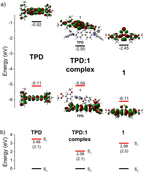
-6 -5 -4 -3 -2 -1
1
TPD:1
complex
-0.92 -2.50 -2.45 -6.11 -5.09 Energy (eV) -5.11TPD
TPD TPD 1 1 a) 0 1 2 3 4 b) Energy (eV)S0 S0 S0
3.48 (3.1) 2.99 (2.5) 2.06 (2.1) S1 S1 1 TPD:1 complex TPD S1
Fig. 3 a) Kohn-Sham molecular orbital diagram and orbital graphical representations
(HOMO and LUMO) of TPD, 1 and of the complex TPD:1 calculated at the PBE0/6-311G(d,p) level of theory (isosurface 0.02). b) First singlet excited state energies calculated at the PBE0/6-311G(d,p) level of theory for TPD, 1 and for the complex
TPD:1; the figures in parentheses are the energy levels determined experimentally.
sought-for energy minimum. The HOMO and LUMO orbitals are widely delocalised on the π backbone for 1 and TPD, with their energy gaps agreeing qualitatively with the experimental data (Fig. 3a). The TPD:1 complex shows a LUMO localised on
1 and a HOMO localised on the TPD molecule. The
reorganisation energies for electrons (𝜆𝑒) and holes (𝜆ℎ) were
calculated theoretically59 for 1. The values obtained for 𝜆𝑒 =
0.425 eV and 𝜆ℎ = 0.384 eV agree qualitatively with the
experimental observations, as the reorganisation energy for the electrons is slightly higher than the corresponding value for holes. Note that the lower the 𝜆 value, the higher the charge-transport rate.59 The first 20 singlet vertical transitions
[image:4.595.307.545.207.494.2]Journal Name ARTICLE
Please do not adjust margins
complex are reported in Fig. 3b. They agree qualitatively, by the levels of relative disposition, with the experimental PL emission maxima of thin films of the mixture of TPD:1 and compound 1, and from the literature data for the film of TPD.60
The recombination process of an electron–hole pair with the electron located on the LUMO of 1 and the hole located on the HOMO of TPD should then be responsible for the EL maximum at ca. 580 nm for the device and explains the exciplex nature of this transition. Here the exciplex is considered as an excited state complex that is formed by an electronically excited state donor molecule (or acceptor) with a complementary acceptor molecule (or donor) in their ground state.61
Conclusions
A WOLED containing the small and simple organic molecule 1 was fabricated. The resulting electroluminescence was shown to be a combination of the exciton/electromer emission of 1 and of the exciplex/electroplex emission at the heterojunction between 1 and TPD. The device has a maximum current efficiency of 6.5 cd/A, a maximum brightness of 5219 cd/m2
and good colour quality with C.I.E. 1931 coordinates (0.38, 0.45) at 15 V and a colour temperature of 4500K.
Acknowledgements
The authors would like to thank the UK Engineering and Physical Sciences Research Council (Grant No: EP/I012591/1), the European Commission (Marie Curie Action of FP7, Grant No: PIRSES-GA-2013-612670), the University of Strathclyde, the Lviv Polytechnic National University and the Kaunas University of Technology for the financial support. We thank the EPSRC UK National mass spectrometry facility for the HRMS measurements. PJS thanks the Royal Society for a Wolfson Research Merit Award.
References
1. Y. Takei, Sci. Technol. Trends–Quarterly Rev., 2009, 32, 59.
2. M. Bessho and K. Shimizu, Electron. Comm. Jpn., 2012, 95, 1.
3. J. Kalinowski, V. Fattori, M. Cocchi and J. A. G. Williams, Coord. Chem. Rev., 2011, 255, 2401.
4. J. Roncali, Macromol. Rapid Commun., 2007, 28, 1761.
5. S. Mukherjee and P. Thilagar, Dyes Pigm., 2014, 110, 2.
6. K. Bando, K. Sakano, Y. Noguchi and Y. Shimizu, J. Light & Vis. Env., 1998, 22, 2.
7. R.-J. Xie, N. Hirosaki, M. Mitomo, Y. Yamamoto, T. Suehiro and K. Sakuma, J. Phys. Chem. B, 2004, 108, 12027.
8. R.-J. Xie, N. Hirosaki, K. Sakuma, Y. Yamamoto and M. Mitomo, Appl. Phys. Lett., 2004, 84, 5404.
9. J. K. Sheu, S. J. Chang, C. H. Kuo, Y. K. Su, L. W. Wu, Y. C. Lin, W. C. Lai, J. M. Tsai, G. C. Chi and R. K. Wu, IEEE Photon. Technol. Lett., 2003, 15, 18.
10. W.-J. Yang, L. Luo, T.-M. Chen and N.-S. Wang, Chem. Mater., 2005, 17, 3883.
11. K. T. Kamtekar, A. P. Monkman and M. R. Bryce, Adv. Mater., 2010, 22, 572.
12. C. Tang, X.-D. Liu, F. Liu, X.-L. Wang, H. Xu and W. Huang, Macromol. Chem. Phys., 2013, 214, 314.
13. M. C. Gather, A. Köhnen and K. Meerholz, Adv. Mater., 2011,
23, 233.
14. N. Thejo Kalyani and S. J. Dhoble, Renew. Sust. Energ. Rev., 2012, 16, 2696.
15. I. Moreno and U. Contreras, Opt. Express, 2007, 15, 3607.
16. N. J. Findlay, J. Bruckbauer, A. R. Inigo, B. Breig, S. Arumugam, D. J. Wallis, R. W. Martin and P. J. Skabara, Adv. Mater., 2014, 26, 7290.
17. G. Giro, M. Cocchi, J. Kalinowski, P. Di Marco and V. Fattori, Chem. Phys. Lett., 2000, 318, 137.
18. P. Nandhikonda and M. D. Heagy, Chem. Commun., 2010, 46, 8002.
19. P. Nandhikonda and M. D. Heagy, Org. Lett., 2010, 12, 4796.
20. D. Liu, Z. Zhang, H. Zhang and Y. Wang, Chem. Commun., 2013,
49, 10001.
21. K.-C. Tang, M.-J. Chang, T.-Y. Lin, H.-A. Pan, T.-C. Fang, K.-Y. Chen, W.-Y. Hung, Y.-H. Hsu and P.-T. Chou, J. Am. Chem. Soc., 2011,
133, 17738.
22. Y. Zhao, L. Duan, X. Zhang, D. Zhang, J. Qiao, G. Dong, L. Wang and Y. Qiu, RSC Adv., 2013, 3, 21453.
23. J. Karpiuk, E. Karolak and J. Nowacki, Phys. Chem. Chem. Phys., 2010, 12, 8804.
24. V. Jankus, P. Data, D. Graves, C. McGuinness, J. Santos, M. R. Bryce, F. B. Dias and A. P. Monkman, Adv. Funct. Mater., 2014, 24, 6178.
25. T. Ishisone, S. Seo, Y. Nonaka, T. Kawata and N. Ohsawa, J. Soc. Inf. Display, 2014, 22, 404.
26. V. Cherpak, P. Stakhira, B. Minaev, G. Baryshnikov, E. Stromylo, I. Helzhynskyy, M. Chapran, D. Volyniuk, Z. Hotra, A. Dabuliene, A. Tomkeviciene, L. Voznyak and J. V. Grazulevicius, ACS Appl. Mater. Interfaces, 2015, 7, 1219.
ARTICLE Journal Name
6 | J. Name., 2012, 00, 1-3 This journal is © The Royal Society of Chemistry 20xx
Please do not adjust margins
Please do not adjust margins
28. J.-Y. Hu, Y.-J. Pu, Y. Yamashita, F. Satoh, S. Kawata, H. Katagiri,H. Sasabe and J. Kido, J. Mater. Chem. C, 2013, 1, 3871.
29. J.-Y. Hu, Y.-J. Pu, G. Nakata, S. Kawata, H. Sasabe and J. Kido, Chem. Commun., 2012, 48, 8434.
30. M. Sharnoff, J. Lumin., 1971, 4, 69.
31. S. Yang and M. Jiang, Chem. Phys. Lett., 2009, 484, 54.
32. Y. Liu, J. Guo, H. Zhang and Y. Wang, Angew. Chem. Int. Ed., 2002, 41, 182.
33. D. Rankine, A. Avellaneda, M. R. Hill, C. J. Doonan and C. J. Sumby, Chem. Commun., 2012, 48, 10328.
34. J.-M. Raimundo, P. Blanchard, H. Brisset, S. Akoudad and J. Roncali, Chem. Commun., 2000, 939.
35. B. A. D. Neto, A. A. M. Lapis, E. N. da Silva Júnior and J. Dupont, Eur. J. Org. Chem., 2013, 2013, 228.
36. S.-i. Kato, T. Matsumoto, T. Ishi-i, T. Thiemann, M. Shigeiwa, H. Gorohmaru, S. Maeda, Y. Yamashita and S. Mataka, Chem. Commun., 2004, 2342.
37. M. Akhtaruzzaman, N. Kamata, J.-i. Nishida, S. Ando, H. Tada, M. Tomura and Y. Yamashita, Chem. Commun., 2005, 3183.
38. D. Aldakov, M. A. Palacios and P. Anzenbacher, Chem. Mater., 2005, 17, 5238.
39. W. Rettig, Angew. Chem. Int. Ed., 1986, 25, 971.
40. J. R. Lakowicz and A. Balter, Photochem. Photobiol., 1982, 36, 125.
41. G. Weber and F. J. Farris, Biochemistry, 1979, 18, 3075.
42. P. Ledwon, N. Thomson, E. Angioni, N. J. Findlay, P. J. Skabara and W. Domagala, RSC Adv., 2015, 5, 77303.
43. K. M. Omer, S.-Y. Ku, K.-T. Wong and A. J. Bard, J. Am. Chem. Soc., 2009, 131, 10733.
44. G. M. Saltan, H. Dinçalp, M. Kıran, C. Zafer and S. Ç. Erbaş, Mater. Chem. Phys., 2015, 163, 387.
45. J. L. Bredas, R. Silbey, D. S. Boudreaux and R. R. Chance, J. Am. Chem. Soc., 1983, 105, 6555.
46. J. Sworakowski and J. Ulanski, Annu. Rep. Prog. Chem., Sect. C: Phys. Chem., 2003, 99, 87.
47. J. C. Blakesley, F. A. Castro, W. Kylberg, G. F. A. Dibb, C. Arantes, R. Valaski, M. Cremona, J. S. Kim and J.-S. Kim, Org. Electron., 2014,
15, 1263.
48. S. R. Tseng, Y. S. Chen, H. F. Meng, H. C. Lai, C. H. Yeh, S. F. Horng, H. H. Liao and C. S. Hsu, Synth. Met., 2009, 159, 137.
49. J. Kalinowski, M. Cocchi, D. Virgili, V. Fattori and J. A. G. Williams, Adv. Mater., 2007, 19, 4000.
50. Y.-H. Lee, T.-C. Wu, C.-W. Liaw, T.-C. Wen, S.-W. Feng, J.-J. Lee, Y.-T. Wu and T.-F. Guo, Org. Electron., 2013, 14, 1064.
51. J. Kalinowski, Mater. Sci.-Poland, 2009, 27, 735.
52. S. Kwon, K.-R. Wee, C. Pac and S. O. Kang, Org. Electron., 2012,
13, 645.
53. J. Kalinowski, G. Giro, M. Cocchi, V. Fattori and P. Di Marco, Appl. Phys. Lett., 2000, 76, 2352.
54. G. M. Farinola and R. Ragni, Chem. Soc. Rev., 2011, 40, 3467.
55. Q. Wang and D. Ma, Chem. Soc. Rev., 2010, 39, 2387.
56. G. M. Farinola and R. Ragnar, Chem. Soc. Rev., 2011, 40, 3467.
57. R. Improta, V. Barone, G. Scalmani and M. J. Frisch, J. Chem. Phys., 2006, 125, 054103.
58. F. Furche and R. Ahlrichs, J. Chem. Phys., 2002, 117, 7433.
59. L.-Y. Zou, A.-M. Ren, J.-K. Feng and X.-Q. Ran, J. Phys. Org. Chem., 2009, 22, 1104.
60. H. Mattoussi, H. Murata, C. D. Merritt, Y. Iizumi, J. Kido and Z. H. Kafafi, J. Appl. Phys., 1999, 86, 2642.
Electronic Supplementary Information Section
A single emitting layer white OLED based on exciplex interface emission
Enrico Angioni, Marian Chapran, Khrystyna Ivaniuk, Nataliya Kostiv, Vladyslav Cherpak,*
Pavlo Stakhira, Algirdas Lazauskas, Sigitas Tamulevičius, Dmytro Volyniuk, Neil J. Findlay,
Tell Tuttle, Juozas V. Grazulevicius,* Peter J. Skabara*
General Experimental
All reactions were performed using vacuum Schlenk lines, in an inert atmosphere of nitrogen.
Dry solvents were obtained from a solvent purification system (SPS 400 from Innovative
Technologies) using alumina as the drying agent. The compounds 4-iodo-3-hydroxybenzoic
acid,
1methyl 4-iodo-3-hydroxybenzoate,
1methyl 4-iodo-3-methoxybenzoate (
2
)
1were
synthesised and analysed using literature procedures. All the other reagents were purchased
from Sigma Aldrich or Alfa Aesar and used without further purifications.
1H and
13C NMR
spectra were recorded on a Bruker Avance DPX400 apparatus at 400.1 and 100.6 MHz.
Chemical shifts are given in ppm; all
J
values are in Hz. MS LDI-TOF spectra were run on a
Shimadzu Axima-CFR spectrometer (mass range 1-150000 Da). The high resolution mass
measurements were performed on the Thermo Scientific LTQ ORBITRAP XL instrument,
using the nano-electrospray ionisation (nano-ESI) technique. Thermogravimetric analysis
(TGA) was performed using a Perkin-Elmer Thermogravimetric Analyser TGA7 under a
constant flow of argon. Melting points were taken using a TA instruments DSC QC1000
Differential Scanning Calorimeter. Cyclic voltammetry (CV) measurements were performed
on a CH Instruments 660A electrochemical workstation with
i
R compensation using
anhydrous dichloromethane as the solvent. The electrodes were glassy carbon, platinum wire
and silver wire as the working, counter and reference electrodes, respectively. All solutions
were degassed (Ar) and contained the substrate in concentrations of
ca
. 10
-4M, together with
n-Bu
4NPF
6(0.1M) as the supporting electrolyte. All measurements are referenced against the
E
1/2of the F
c/F
c+redox couple. Absorption spectra were recorded on a Shimadzu UV 2700
instrument. Photoluminescence measurements were recorded using a Perkin-Elmer LS 50 B
fluorescence spectrometer in a quartz cuvette (path length 10 mm). Absolute
photoluminescence quantum yield measurements were measured according to the de Mello
22
Halogen lamp by using a Gooch & Housego spectrometer and the emission light was
collected by Ocean optics USB 2000 spectrometer. Measurements were performed in air. The
ionisation potential of
1
was measured by the electron photoemission method in air.
3The
samples were fabricated by means of vacuum deposition of
1
onto an indium tin oxide (ITO)
coated glass substrate. The experimental setup consists of the deep-UV deuterium light
source ASBN-D130-CM, the CM110 1/8m monochromator, and the 6517B Keithley
electrometer. Characteristics of the current density−voltage and luminance−voltage
dependences were measured with a semiconductor parameter analyser (HP 4145A) using it in
air without passivation immediately after fabrication of the device. The measurement of
brightness was performed using a calibrated photodiode.
4Calibration of the photodetector
was carried out using a radiometer RTN 20 (accuracy ±2%). The photodiode was placed in
front of the OLED in a dark room and the calibration was performed according to the method
described earlier.
5The external quantum efficiency (EQE) values were determined using the
equations given in reference 6. The OLED electroluminescence and photoluminescence (PL)
spectra of the solid films were recorded with an Ocean Optics USB2000 spectrometer. For
the spectral studies the single layers of
1
as well as the
1
:
TPD
composite layer were prepared
by thermovacuum deposition at 10
-6Torr onto clean quartz substrates or spin coating
ca.
2M
solutions of
1
as well as
1
/
TPD
onto clean quartz substrates. Luminescence spectra and
luminescence decay curves of the layers were recorded with an Edinburgh Instruments
FLS980 spectrometer at 77 K and room temperature using a low repetition rate μF920H
Xenon Flashlamp as the excitation source. The emission was measured twice: immediately
after excitation and with a delay after the pulse was turned off (the delay time was set to be
ca.
30 μs). Chromaticity coordinates (CIE 1931) and correlated colour temperatures (CCT)
are calculated from the response-corrected spectra. X-ray diffraction measurements at grazing
incidence (XRDGI) were performed using a D8 Discover diffractometer (Bruker) with Cu K
α(λ= 1.54 Å) X-ray source. Parallel beam geometry with a 60 mm Göbel mirror (X-ray mirror
on a high precision parabolic surface) was used. This configuration enables transforming the
divergent incident X-ray beam from a line focus of the X-ray tube into a parallel beam that is
free of K
βradiation. The primary side also had a Soller slit with an axial divergence of 2.5º.
and auto-repeat function enabled. The resultant diffractograms were processed with the
software DIFFRAC.EVA. AFM experiments were carried out in air at room temperature
using a NanoWizardIII atomic force microscope (JPK Instruments), while data were analysed
using SurfaceXplorer and JPKSPM Data Processing software. AFM images were collected
using a V-shaped silicon cantilever (spring constant of 3 N/m, tip curvature radius of 10.0 nm
and the cone angle of 20º) operating in contact mode. The space-charge-limited current
(SCLC) measurements were adopted for the estimation of charge drift mobility of
1
.
Hole-only and electron-Hole-only devices were fabricated as described in the paper. The current density
vs. voltage characteristics of the hole-only and electron-only devices were recorded and fitted
using the Mott-Gurney law:
7𝐽
𝑆𝐶𝐿𝐶= 𝜇
09
8
𝑉
𝑑
32
𝜀𝜀
0(0.891𝛾√𝑉/𝑑)
(1)
J
SCLCis the steady-state current density;
μ
0is the zero field mobility;
V
is applied voltage;
d
is
the film thickness,
ε
is the permittivity of the film (~3); ε
0is the vacuum permittivity and γ is
the field dependence parameter. The ITO-coated glass substrates had a sheet resistance of 15
Ω/sq and the organic layers were deposited in top of it at a rate < 0.1Å/s, using a MB
EcoVap4G vacuum deposition system build in a Kurt J. Lesker glove box. The sample area
was of 6 mm
2. The charge drift mobility of
1
was estimated as previously described from J.
C. Blakesley
et al
.
8All the theoretic calculations were performed with the software package
Gaussian09 (Revision A.02).
9Synthesis of dimethyl 4,4'-(benzo[c][1,2,5]thiadiazole-4,7-diyl)bis(3-methoxybenzoate) (1)
4
afford a dark yellow solid. Purification on silica gel, eluting dichloromethane to wash off the
impurities and then chloroform afforded a dark yellow powder. The title compound (
1
) was
obtained after recrystallisation from hot acetone as a bright yellow powder (69 mg, 58%).
TGA: 5% mass loss at 311 °C; T
m= 227 °C, T
c= 147 °C;
1H NMR (400.1 MHz, CDCl
3, δ)
7.81 (dd,
J
= 7.8, 1.5 Hz, 2H, Ar H), 7.77 (d,
J
= 1.5 Hz, 2H, Ar H), 7.76 (s, 2H, Ar H), 7.65
(d,
J
= 7.8 Hz, 2H, ArH), 3.97 (s, 6H, COOCH
3), 3.88 (s, 6H, OCH
3);
13C NMR (100.6 MHz,
CDCl
3, δ) 166.9, 157.2, 154.1, 131.9, 131.5, 131.2, 130.5, 129.9, 122.1, 112.4, 56.1, 52.4;
MALDI (m/z (%)) 464.15 (100), 465.12 (75), 466.14 (30); HRMS (LSI-TOF)
m/z
[M + H]
+ [image:10.595.73.534.380.703.2]calcd for C
24H
21N
2O
6S 465.1115, found 465.1117. Melting Point: 230-232 °C.
Table S1.
Energies, wavelengths, oscillator strengths, symmetry and orbital assignments of
the first 20 singlet vertical electronic transitions for
1
(vacuum) calculated at the
PBE0/6-311G(d,p) level of theory.
Energy (eV)
Wavelengt h (nm)
Oscillato r Strength
Symmetry Major contributions
2.99 415.0 0.4026 Singlet HOMO->LUMO (98%) 3.49 355.3 0.0074 Singlet H-1->LUMO (99%) 3.74 331.3 0.0267 Singlet H-2->LUMO (96%) 3.98 311.2 0.6020 Singlet HOMO->L+1 (95%)
4.12 300.9 0.0058 Singlet H-3->LUMO (74%), HOMO->L+2 (13%) 4.33 286.1 0.0636 Singlet H-4->LUMO (25%), HOMO->L+2 (63%)
4.48 276.7 0.0509 Singlet H-4->LUMO (52%), H-1->L+1 (12%), HOMO->L+2 (10%) 4.55 272.4 0.0443 Singlet H-1->L+1 (64%), HOMO->L+2 (10%)
4.62 268.6 0.0248 Singlet H-2->L+1 (50%), H-1->L+2 (31%) 4.73 262.2 0.0178 Singlet H-5->LUMO (89%)
4.74 261.4 0.0002 Singlet H-8->LUMO (43%), H-6->LUMO (32%)
4.78 259.3 0.0002 Singlet H-7->LUMO (63%), H-7->L+1 (14%), H-6->L+2 (17%)
4.81 257.9 0.0000 Singlet H-8->LUMO (33%), H-7->L+2 (13%), H-6->LUMO (31%), H-6->L+1 (12%) 4.98 249.1 0.0460 Singlet H-2->L+1 (36%), H-1->L+2 (61%)
5.00 248.0 0.0001 Singlet H-3->L+1 (11%), H-2->L+2 (59%), H-1->L+1 (17%) 5.05 245.8 0.0027 Singlet H-11->LUMO (79%)
-2.0 -1.5 -1.0 -0.5 0.0 0.5 1.0 1.5 2.0
-40
-20
0
20
40
60
80
100
120
140
160
180
Intensity (
A)
[image:11.595.139.431.91.314.2]Potential (V)
Figure S1.
Cyclic voltammogram of
1
(1·10
-4M solution). Measurements performed using a
glassy carbon working electrode, Ag/AgCl reference electrode and platinum wire counter
electrode. The supporting electrolyte was 0.1M tetrabutylammonium hexafluorophosphate in
dichloromethane. Scan rate of 0.1 Vs
-1. All the waves were referenced to ferrocene.
5.6 5.8 6.0 6.2 6.4 6.6
0.0 0.1 0.2 0.3 0.4 0.5
Photon energy
(eV)
i
0.5
(a.u.)
[image:11.595.158.409.448.631.2]6
Figure S3
. AFM 3D topographical images with normalized Z axis in nm of thin films (30
nm) of
1
prepared by vacuum evaporation at different deposition rates on glass substrates: (a)
<0.1Å/s, (b) 1.5 Å/s and (c) 10 Å/s. The images were acquired in air using contact mode.
Figure S4.
X-ray diffraction patterns a grazing incidence angle of 1.50º of thin films of
1
prepared by vacuum evaporation at different deposition rates on glass substrates: (a) <0.1Å/s,
(b) 1.5 Å/s and (c) 10 Å/s.
In
te
ns
ity
(a
rb
. u
ni
ts
)
2
θ
(degree)
20 40 60 80 100 120
(a)
In
te
ns
ity
(a
rb
. u
ni
ts
)
(b)
2
θ
(degree)
20 40 60 80 100 120
In
te
ns
ity
(a
rb
. u
ni
ts
)
(c)
2
θ
(degree)
20 40 60 80 100 120
In
te
ns
ity
(a
rb
. u
ni
ts
)
2
θ
(degree)
20 40 60 80 100 120
(a)
In
te
ns
ity
(a
rb
. u
ni
ts
)
(b)
2
θ
(degree)
20 40 60 80 100 120
In
te
ns
ity
(a
rb
. u
ni
ts
)
(c)
2
θ
(degree)
[image:13.595.173.422.72.565.2]8
0
1
2
3
4
5
6
7
8
9
10
0
1
2
3
4
5
6
7
8
hole-only device
electron-only device
fitting
Current density (mA/cm
2
)
Voltage (V)
Figure S5
Current density-voltage characteristic curves and fittings of the hole only and
electron only devices. The disagreement between the experimental and fit curves can be
explained taking in account the existence of electron and hole traps in
1
due to its
morphology.
600
700
800
900
1000
10
-710
-6Holes
Electrons
SCLC(cm
2
V
-1s
-1)
E
1/2(V
1/2cm
-1/2)
[image:14.595.144.431.86.315.2] [image:14.595.136.438.472.702.2]-7
-6
-5
-4
-3
-2
-1
Ca
TPD
CuI
ITO
-7.0
-6.0
-5.5
-5.2
-4.7
-2.9
-3.5
-2.9
-2.3
-2.1
CuI
TPD
1
BCP
Energy (eV)
Exci
pl
ex
Figure S7.
Energy-band diagram of the fabricated device. Aluminium was used on the
cathode for the passivation of the calcium electrode, in order to investigate the properties of
the device in ambient atmosphere at room temperature immediately after device fabrication.
400 500 600 700 800
0.0 0.2 0.4 0.6 0.8
1.0 EL of the device at 17 V
Fitting:
Peak1: Fluorescence of 1 at 490 nm Peak2: Electromer at ca. 520 nm Peak3: Exciplex at ca. 580 nm Peak4: Electroplex at 635 nm
PeakSum: Overlapping of the forth peaks
Int
en
sity (a.
u.)
[image:15.595.164.430.85.256.2]Wavelength (nm)
[image:15.595.98.401.358.558.2]10
0.0 0.2 0.4 0.6 0.8
0.0 0.2 0.4 0.6
0.8 8 V 10 V
12 V 14 V 15 V 16 V 17V
y
x
a)
0.30 0.35 0.40 0.45 0.50
0.40 0.45 0.50
b)
8 V10 V 12 V 14 V 15 V 16 V 17V
y
[image:16.595.103.491.82.266.2]x
[image:16.595.193.402.334.471.2]Figure S9
The different colour coordinates of the device under different applied voltages.
Table S2.
The different colour coordinates of the device under different applied voltages.
Applied voltage (V) CIE 1931 coordinates
8 (0.42, 0.44)
10 (0.40, 0.45)
12 (0.39, 0.44)
14 (0.39, 0.45)
15 (0.38, 0.45)
16 (0.38, 0.44)
17 (0.37, 0.44)
Table S3.
Summary of the characteristics of the device.
Von at
1.4 Cd/m2
(V)
Max Brightness
(cd/m2)
Max current efficiency
(cd/A)
Max power Efficiency (lm/W)
Max external Quantum efficiency (%)
CIE 1931 Coordinates
(x, y)
Colour Temperature
(K)
5.8 5219 6.5 2.6 2.39 (0.39, 0.44) 4500
Table S4.
Current efficiency, power efficiency and external quantum efficiency of the device
at different current densities and brightness.
Current density Current efficiency (cd/A) Power efficiency (lm/W) External quantum efficiency (%)
10 mA/cm2 6.23 1.96 2.3
100 mA/cm2 3.99 2.57 1.47
Brightness
100 Cd/m2 6.55 0.96 2.42
[image:16.595.67.529.524.584.2] [image:16.595.66.530.651.738.2]5 7 9 11 13 15 0
20 40 60 80 100 120 140 160
Brightnes
s
(cd/m
2
)
Current dens
ity
(m
A/cm
2
)
Voltage (V)
101
102
103
104
Figure S10.
Current density−voltage and luminance−voltage characteristics of the device.
0 20 40 60 80 100 120 140
0.2 0.4 0.6 0.8 1.0 1.2 1.4 1.6 1.8 2.0 2.2 2.4 2.6 2.8 3.0
Current density mA/cm
2Power effic
ienc
y (Lm
/ W)
Quantum
effic
ienc
y (%
)
0.2 0.4 0.6 0.8 1.0 1.2 1.4 1.6 1.8 2.0 2.2 2.4 2.6 2.8 3.0
[image:17.595.169.429.86.272.2] [image:17.595.173.425.326.503.2]12
0 20 40 60 80 100 120
0 1 2 3 4 5 6 7
Current effi
ci
ency
(cd/A)
Current density (mA/cm
2)
[image:18.595.178.392.87.268.2]Table S5.
Mean signed and mean square errors (MSiE and MSqE, eV) and maximal
deviations (Max-Min, eV), obtained by comparing experimental and theoretical mean
maximum absorption values of literature compound 4,7-dithiophenyl-benzothiadiazole (
3
).
10Using the TD-DFT method including the polarisable continuum model (PCM)
11(dichloromethane) the vertical transitions were calculated for
3
, using the combination of five
different functionals (B3LYP
12, wB97xD,
13CAM-B3LYP,
14M06-2X,
15PBE0)
16and three
different basis sets (6-31G, 6-311G(d,p), 6-311+G(2d,p), DGDZVP). Six vertical absorptions
were simulated at each level of theory and they were fitted with Gaussian curves (full width
at half maximum (FWHM) = 0.37 eV) using the software GaussSum 3.0.
17The two maxima
obtained with this procedure were compared with the experimental maxima absorption bands
of
3
. The level of theory PBE0/6-311G(d,p) have shown the smallest mean signed and mean
square errors (the smallest shift of the vertical absorptions calculated in comparison with the
experimental data) and it was used for all further calculations.
B3LYP wB97X-D
6-31G 6-311G(d,p) 6-311+G(2d,p) DGDZVP 6-31G 6-311G(d,p) 6-311+G(2d,p) DGDZVP
MSiE -0.323 -0.281 -0.319 -0.397 0.463 0.475 0.436 0.436
MSqE 0.113 0.087 0.109 0.166 0.231 0.241 0.199 0.202
Max(+) -0.228 -0.190 -0.236 -0.306 0.593 0.601 0.531 0.546
Min(-) -0.418 -0.372 -0.402 -0.488 0.334 0.349 0.341 0.326
CAM-B3LYP M06-2X
6-31G 6-311G(d,p) 6-311+G(2d,p) DGDZVP 6-31G 6-311G(d,p) 6-311+G(2d,p) DGDZVP
MSiE 0.363 0.405 0.359 0.316 0.363 0.421 0.351 0.335
MSqE 0.155 0.182 0.139 0.117 0.160 0.197 0.134 0.130
Max(+) 0.515 0.539 0.461 0.446 0.531 0.562 0.453 0.469
Min(-) 0.210 0.272 0.256 0.186 0.194 0.279 0.248 0.202
PBE0
6-31G 6-311G(d,p) 6-311+G(2d,p) DGDZVP
MSiE -0.153 -0.114 -0.153 -0.153
MSqE 0.037 0.025 0.032 0.034
M
ax(+) -0.035 -0.004 -0.058 -0.050
14
a
e
b
f
c
g
[image:20.595.79.524.72.725.2]d
h
Table S6.
Relative total energies for height different
TPD:1
complexes (
a-h
), calculated at
the PBE0/6-311G(d,p) level of theory.
Complex Relative total energy (kcal/mol)
a 0.00
b 2.42
c 2.97
d 3.40
e 1.30
f 3.95
g 1.92
h 3.29
1
TPD
[image:21.595.79.513.320.448.2]16
Table S7.
Energies, wavelengths, oscillator strengths, symmetry and orbital assignments of
the first 20 singlet vertical electronic transitions for
TPD
(vacuum) calculated at the
PBE0/6-311G(d,p) level of theory.
Energy (eV)
Wavelength (nm)
Oscillator
Strength Symmetry Major contributions
3.48 356.0 1.0686 Singlet HOMO->LUMO (96%)
3.78 328.0 0.0097 Singlet H-1->L+2 (14%), HOMO->L+1 (83%) 3.84 323.3 0.0191 Singlet H-1->L+1 (21%), HOMO->L+2 (75%) 3.95 313.8 0.0005 Singlet H-1->LUMO (95%)
4.03 307.5 0.1855 Singlet H-1->L+3 (17%), HOMO->L+3 (78%) 4.05 306.2 0.1792 Singlet H-1->L+4 (16%), HOMO->L+4 (80%) 4.36 284.5 0.0661 Singlet H-1->L+2 (27%), HOMO->L+6 (56%) 4.42 280.7 0.0005 Singlet H-1->L+1 (72%), HOMO->L+2 (19%) 4.46 277.8 0.0009 Singlet HOMO->L+5 (52%), HOMO->L+8 (13%)
4.48 277.0 0.0182 Singlet H-1->L+6 (15%), HOMO->L+7 (43%), HOMO->L+8 (11%), HOMO->L+9 (10%)
4.51 275.1 0.0366 Singlet H-1->L+8 (13%), HOMO->L+7 (21%), HOMO->L+9 (42%) 4.53 274.0 0.0041 Singlet H-1->L+2 (49%), HOMO->L+1 (11%), HOMO->L+6 (23%) 4.59 270.3 0.0002 Singlet HOMO->L+5 (35%), HOMO->L+8 (43%)
4.64 267.5 0.0403 Singlet H-1->L+3 (79%), HOMO->L+3 (18%) 4.65 266.5 0.0387 Singlet H-1->L+4 (81%), HOMO->L+4 (17%) 4.67 265.7 0.0262 Singlet H-1->L+5 (83%)
4.69 264.4 0.0014 Singlet H-1->L+6 (74%), HOMO->L+9 (11%)
4.70 263.6 0.0058 Singlet H-1->L+7 (31%), H-1->L+9 (43%), HOMO->L+6 (13%)
4.80 258.2 0.0201 Singlet H-2->LUMO (16%), H-1->L+8 (38%), HOMO->L+7 (11%), HOMO->L+10 (13%)
Table S8.
Energies, wavelengths, oscillator strengths, symmetry and orbital assignments of
the first 20 singlet vertical electronic transitions for the complex
TPD:1
(vacuum) calculated
at the PBE0/6-311G(d,p) level of theory. It is assumed that emission can be generated from
all the excited state energy levels.
Energy (eV)
Wavelength (nm)
Oscillator
Strength Symmetry Major contributions
2.06 600.7 0.0001 Singlet HOMO->LUMO (95%) 2.44 508.7 0.0000 Singlet H-1->LUMO (94%) 2.99 414.0 0.3039 Singlet H-2->LUMO (98%) 3.09 401.7 0.0010 Singlet HOMO->L+1 (95%)
3.33 372.9 0.0020 Singlet H-1->L+1 (30%), HOMO->L+2 (67%) 3.49 355.1 0.0199 Singlet H-4->LUMO (48%), H-3->LUMO (48%) 3.51 353.3 0.0006 Singlet H-1->L+1 (65%), HOMO->L+2 (25%) 3.54 350.3 0.7465 Singlet HOMO->L+3 (93%)
3.70 335.2 0.0080 Singlet H-5->LUMO (10%), H-4->LUMO (34%), H-3->LUMO (34%) 3.74 331.8 0.0142 Singlet H-7->LUMO (36%), H-1->L+2 (52%)
3.74 331.5 0.0215 Singlet H-7->LUMO (40%), H-1->L+2 (30%)
3.75 330.6 0.0042 Singlet H-6->LUMO (23%), H-5->LUMO (45%), HOMO->L+4 (12%) 3.78 328.4 0.0123 Singlet H-1->L+4 (18%), HOMO->L+4 (53%)
3.81 325.4 0.0265 Singlet H-1->L+5 (13%), HOMO->L+5 (74%) 3.82 324.8 0.0061 Singlet H-1->L+3 (83%)
3.83 324.1 0.0016 Singlet H-9->LUMO (26%), H-6->LUMO (28%), H-5->LUMO (24%) 3.86 321.0 0.5182 Singlet H-2->L+1 (87%)
3.90 318.1 0.0003 Singlet H-8->LUMO (80%)
18
LUMO+2
(-0.046 eV)
HOMO
(-0.187 eV)
LUMO +1
(-0.055 eV)
HOMO -1
(-0.200 eV)
LUMO
(-0.092 eV)
HOMO -2
(-0.227 eV)
[image:24.595.74.530.69.598.2]100
200
300
400
0
20
40
60
80
100
Weight %
Temperature (°C)
Figure S16.
Thermogravimetric analyses of
1
in Argon (40-450°C). The small increment in
the mass of the sample that is observed between 50 and 250°C is likely due to the
Archimede’s effect. When the object is under a current of fluid (nitrogen), the fluid tends to
force the object upwards. When the analyser was tared the fluid (N
2) likely forced the sample
[image:25.595.145.429.89.310.2]20
[image:26.595.74.526.70.385.2]Figure S17.
1H NMR spectrum of
1
recorded in deuterated chloroform.
[image:26.595.75.522.419.739.2]References
1 D. Rankine, A. Avellaneda, M. R. Hill, C. J. Doonan, C. J. Sumby, Chem. Commun., 2012, 48, 10328. 2 J. C. de Mello, H. F. Wittmann, R. H. Friend, Adv. Mater., 1997, 9, 230.
3 E. Miyamoto, Y. Yamaguchi, M. Yokoyama, J. Imaging Sci. Technol., 1989, 28, 364.
4 V. Cherpak, A. Gassmann, P. Stakhira, D. Volyniuk, J. V. Grazulevicius, A. Michaleviciute, A. Tomkeviciene, G. Barylo, H. von Seggern, Org. Electron., 2014, 15, 1396.
5 N. C. Greenham, R. H. Friend, D. D. C. Bradley, Adv. Mater., 1994, 6, 491.
6 M. A. F. Baldo, S. R.; Thompson, M. E. , Organic Electroluminescence, CRC Press, 2005. 7 N. F. Mott, R. W. Gurney, Electronic Processes in Ionic Crystals, Oxford, 1940.
8 J. C. Blakesley, F. A. Castro, W. Kylberg, G. F. A. Dibb, C. Arantes, R. Valaski, M. Cremona, J. S. Kim, J.-S. Kim, Org. Electron., 2014, 15, 1263.
9 M. J. Frisch, G. W. Trucks, H. B. Schlegel, G. E. Scuseria, M. A. Robb, J. R. Cheeseman, G. Scalmani, V. Barone, B. Mennucci, G. A. Petersson, H. Nakatsuji, M. Caricato, X. Li, H. P. Hratchian, A. F. Izmaylov, J. Bloino, G. Zheng, J. L. Sonnenberg, M. Hada, M. Ehara, K. Toyota, R. Fukuda, J. Hasegawa, M. Ishida, T. Nakajima, Y. Honda, O. Kitao, H. Nakai, T. Vreven, J. A. Montgomery Jr., J. E. Peralta, F. Ogliaro, M. J. Bearpark, J. Heyd, E. N. Brothers, K. N. Kudin, V. N. Staroverov, R. Kobayashi, J. Normand, K. Raghavachari, A. P. Rendell, J. C. Burant, S. S. Iyengar, J. Tomasi, M. Cossi, N. Rega, N. J. Millam, M. Klene, J. E. Knox, J. B. Cross, V. Bakken, C. Adamo, J. Jaramillo, R. Gomperts, R. E. Stratmann, O. Yazyev, A. J. Austin, R. Cammi, C. Pomelli, J. W. Ochterski, R. L. Martin, K. Morokuma, V. G. Zakrzewski, G. A. Voth, P. Salvador, J. J. Dannenberg, S. Dapprich, A. D. Daniels, Ö. Farkas, J. B. Foresman, J. V. Ortiz, J. Cioslowski, D. J. Fox, Gaussian 09, 2009. 10 S.-i. Kato, T. Matsumoto, T. Ishi-i, T. Thiemann, M. Shigeiwa, H. Gorohmaru, S. Maeda, Y.
Yamashita, S. Mataka, Chem. Commun., 2004, 2342.
11 S. Miertuš, E. Scrocco, J. Tomasi, Chem. Phys., 1981, 55, 117. 12 A. D. Becke, J. Chem. Phys., 1993, 98, 5648.
13 J.-D. Chai, M. Head-Gordon, Phys. Chem. Chem. Phys., 2008, 10, 6615. 14 T. Yanai, D. P. Tew, N. C. Handy, Chem. Phys. Lett., 2004, 393, 51. 15 Y. Zhao, D. Truhlar, Theor. Chem. Acc., 2008, 120, 215.
16 C. Adamo, V. Barone, J. Chem. Phys., 1999, 110, 6158.