City, University of London Institutional Repository
Citation
:
Xu, Quan (2016). Data reliability and error correction for NAND Flash Memory System. (Unpublished Doctoral thesis, City University London)This is the accepted version of the paper.
This version of the publication may differ from the final published
version.
Permanent repository link:
http://openaccess.city.ac.uk/15120/Link to published version
:
Copyright and reuse:
City Research Online aims to make research
outputs of City, University of London available to a wider audience.
Copyright and Moral Rights remain with the author(s) and/or copyright
holders. URLs from City Research Online may be freely distributed and
linked to.
City Research Online: http://openaccess.city.ac.uk/ [email protected]
for NAND Flash Memory System
Pal, Atasi (2013). Thulium-doped fibre laser in the 2 μm wavelength region for gas sensing.
(Unpublished Doctoral thesis, City University London)
City Research Online
Original citation
: Pal, Atasi (2013). Thulium-doped fibre laser in the 2 μm wavelength region for
gas sensing. (Unpublished Doctoral thesis, City University London)
Permanent City Research Online URL
: http://openaccess.city.ac.uk/2989/
Copyright & reuse
City University London has developed City Research Online so that its users may access the
research outputs of City University London's staff. Copyright © and Moral Rights for this paper are
retained by the individual author(s) and/ or other copyright holders. All material in City Research
Online is checked for eligibility for copyright before being made available in the live archive. URLs
from City Research Online may be freely distributed and linked to from other web pages.
Versions of research
The version in City Research Online may differ from the final published version. Users are advised
to check the Permanent City Research Online URL above for the status of the paper.
Enquiries
If you have any enquiries about any aspect of City Research Online, or if you wish to make contact
with the author(s) of this paper, please email the team at
[email protected]
.
Quan Xu
School of Mathematics, Computer Science & Engineering
City University London
This dissertation is submitted for the degree of
Doctor of Philosophy
This thesis is presented in fulfilment of the requirement for the degree of Doctor of
Philosophy. The research reported in this doctoral thesis has been carried out at the City
University London. I declare that except where specific reference is made to the work
of others, the contents of this dissertation are original and have not been submitted in
whole or in part for consideration for any other degree or qualification in this, or any
other university. This dissertation is my own work and contains nothing which is the
outcome of work done in collaboration with others, except as specified in the text and
Acknowledgements.
Quan Xu
I take this opportunity to express my sincere gratitude to my advisor, Professor Tom
Chen, for his continuing guidance, support and encouragement. His enthusiasm and
expertise in the area of signal processing, error correction coding and probability theory
help me better understand the subtle facets of this work. His rigorous attitude toward
science stimulates me throughout the writing of thesis.
I also thank my officemates, Mr Pu Gong, Mr Tareq Alalyani and Dr Jorge Blasco.
Their advice and ideas help me walk forward and are very important to my research.
Working with these colleagues has not only been a good learning experience, but also a
great pleasure. In addition, I acknowledge iStorage Limited and Mr John Michael for
his great support to my research project in flash channel modelling.
I would like to thank the coauthors of my publications for their collaborations.
Special thanks to Dr Yupeng Hu at the Hunan University, and Dr Shancang Li at the
Edinburgh Napier University for their help in applying LDPC coding to the flash storage
error correction. I also acknowledge Qiang Liao, Jian Yu in Initio Corporation for their
valuable advice on the implementation of ECC decoder and the data pattern processing
schemes.
I am sincerely grateful to my parents and my fiancée for always being supportive
and encouraging in my pursuit of academic excellence. Without them, I would not ever
NAND flash memory has been widely used for data storage due to its high density, high
throughput, and low power. However, as the flash memory scales to smaller process
technologies and stores more bits per cell, its reliability is decreasing. The error
correc-tion coding can be used to significantly improve the data reliability; nevertheless, the
advanced ECCs such as low-density parity-check (LDPC) codes generally demand
soft-decisions while NAND flash memory channel provides hard-soft-decisions only. Extracting
the soft information requires the accurate characterization of flash memory channel and
the effective design of coding schemes.
To this end, we have presented a novel LDPC-TCM coding scheme for the
Multi-level Cell (MLC) flash memories. The a posteriori TCM decoding algorithm is used
in the scheme to generate soft information, which is fed to the LDPC decoder for
further correction of data bits. It has been demonstrated that the proposed scheme
can achieve higher error correction performance than the traditional hard-decisions
based flash coding algorithms, and is feasible in the design practice. Further with the
LDPC-TCM, we believe it is important to characterize the flash memory channel and
investigate a method to calculate the soft decision for each bit, with the available channel
outputs. We studied the various noises and interferences occurring in the memory
channel and mathematically formulated the probability density function of the overall
noise distribution. Based on the results we derived the final distribution for the cell
threshold voltages, which can be used to instruct the calculation of soft decisions. The
discoveries on the theoretical level have been demonstrated to be consistent with the real
channel behaviours. The channel characterization and model provided in this dissertation
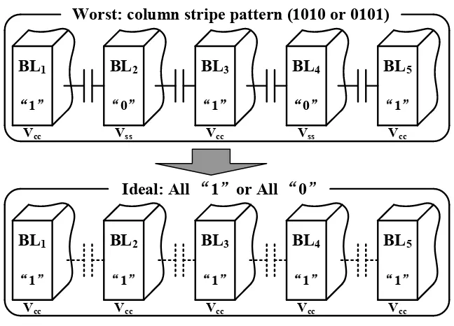
The data pattern processing algorithm deals with the write patterns and targets to
lower the proportion of patterns that would introduce data errors. On the other hand,
the voltages applied to the memory cells charges the MOSFET capacitances frequently
on programming these data patterns, leading to the power problem. The high energy
consumption and current spikes also cause reliability issue to the data stored in the
flash memory. This dissertation proposes a write pattern formatting algorithm (WPFA)
attempting to solve the two problems together. We have designed and implemented
the algorithm and evaluated its performance through both the software simulations and
List of figures ix
List of tables xii
List of Abbreviations xiii
List of Notations xiv
1 Introduction 1
1.1 Motivation . . . 3
1.2 Goals . . . 8
1.3 Thesis Contribution . . . 9
1.4 Thesis Outline . . . 12
2 Background 14 2.1 Basics of NAND Flash Memory . . . 14
2.1.1 NAND Device Organization . . . 15
2.1.2 NAND Cell Architecture and Basic Operations . . . 16
2.1.3 Planar and 3D NAND Flash Memory . . . 21
2.2 Data Reliability Issues . . . 23
2.2.1 Reliability at Physical Level . . . 23
2.2.2 Noises in NAND Flash Memory . . . 24
2.2.3 Error Correction Codes for Flash Memories . . . 30
2.4 Summary and Challenges . . . 34
3 Write Pattern Formatting Algorithm and Implementation 35 3.1 Problem Description . . . 37
3.2 Related Work . . . 40
3.3 Write Pattern Formatting Algorithm . . . 44
3.4 Performance Evaluation . . . 47
3.4.1 Maximum Length of Column Stripe Patterns . . . 47
3.4.2 Average Program Current . . . 48
3.4.3 Proportion of the HighestVthState . . . 50
3.4.4 Overhead of NAND Cell Area . . . 54
3.5 Hardware Design and Implementation Complexity . . . 56
3.5.1 Hardware Implementation of WPFA Encoder and Decoder . . . 58
3.5.2 Analysis of Implementation Complexity . . . 60
3.6 Summary and Challenges . . . 61
4 Concatenated LDPC-TCM Error Correction Coding 64 4.1 Problem Description . . . 65
4.2 Background . . . 67
4.2.1 Basics of Trellis Coded Modulation . . . 68
4.2.2 Low Density Parity Check Codes . . . 74
4.2.3 Related Work . . . 77
4.3 Concatenated LDPC-TCM Coding System . . . 79
4.3.1 System Description . . . 79
4.3.2 Soft Decisions Calculation . . . 82
4.3.3 Theoretical Analysis of Coded Modulation in Flash Memory . . 84
4.4 Performance Evaluation . . . 86
4.5 Summary and Challenges . . . 93
5.2 Background . . . 100
5.2.1 Equivalent Channel Model Incorporated with Major Threshold Voltage Distortions . . . 100
5.2.2 Characteristic Functions of Random Variables . . . 107
5.2.3 Related Work . . . 110
5.3 Characterisation of NAND Flash Memory Channel . . . 111
5.3.1 Overall Distribution of the Noises and Distortions . . . 112
5.3.2 Cell Threshold Voltage Distributions . . . 124
5.4 Calculation of Soft Decisions . . . 127
5.5 Summary and Challenges . . . 129
6 Conclusions and Future Work 131 6.1 Thesis Conclusion . . . 131
6.2 Directions for Future Work . . . 133
References 136
1.1 Overview of the thesis organization. . . 12
2.1 NAND flash memory array structure . . . 16
2.2 Flash memory cell vs. MOSFET. . . 17
2.3 Control-gate voltage in program operation. . . 19
2.4 Read reference voltages for 4-level MLC. . . 20
2.5 A Typical structure of VG flash memory. . . 22
2.6 Capacitors involved in the NAND flash memory channel. . . 25
2.7 Cell to cell coupling trend. . . 26
2.8 Functional representation of a NAND-based memory system. . . 33
3.1 Functions implemented in the flash translation layer. . . 36
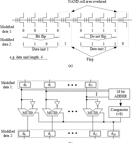
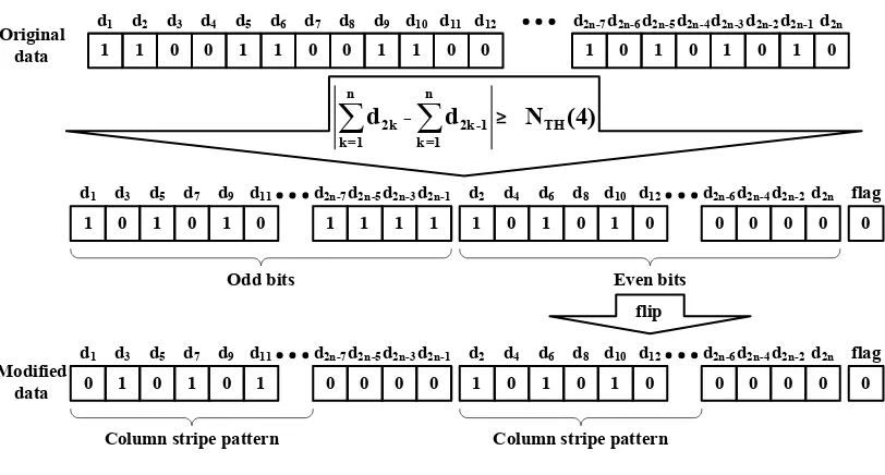
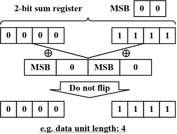
3.2 Example of multipage programming for 2 bits/cell NAND flash memory. 38 3.3 Operation of pre-charging under different programming data patterns . . 40
3.4 (a) Algorithm of the asymmetric coding. (b) Schematic circuit diagram of the asymmetric coding encoder. . . 41
3.5 Example of SPEA. . . 43
3.6 WPFA: lower page data. . . 44
3.7 Analysis of two specific data patterns . . . 45
3.8 WPFA: upper page data. . . 47
3.11 Simulation results of probabilities of “1”s in Tanakamaru’s and the
proposed schemes. . . 53
3.12 Vth distributions of the worst case, randomized interleaving, and the
proposed algorithm. . . 54
3.13 The number of flag bits required for WPFA and Tanakamaru’s algorithm. 55
3.14 The reduced NAND cell area overhead to Tanakamaru’s design. . . 56
3.15 Framework of coding mechanism in SSDs. . . 57
3.16 Circuit schematic of the joint lower/upper pages WPFA encoder . . . . 59
3.17 Circuit schematic of the joint lower/upper pages WPFA decoder . . . . 59
4.1 A general trellis coded modulation . . . 69
4.2 Pragmatic TCM uses a standard rate 1/2 convolutional code. . . 70
4.3 Tanner graph representation for an LDPC code . . . 75
4.4 The approximate flash memory cell threshold voltage distribution model. 80
4.5 Block diagram of TCM LDPC coding system. . . 81
4.6 State transitions in pragmatic TCM. . . 83
4.7 Asymptotic coding gain of TCM for MLC flash memories and M-PAM
modulation. . . 87
4.8 Performance comparisons for the raw BERs of 4 levels, 8 levels MLC
and TCM without quantization. . . 89
4.9 Performance comparisons of the raw BER of 4 levels and the TCM with
quantization . . . 90
4.10 Performance comparisons of the raw BER of 4 levels, the BCH coding
and the TCM for NAND flash memories. . . 91
4.11 Performance comparisons of the raw BER of 4 levels, the BCH coding
and the proposed LDPC-TCM coding. . . 92
4.12 Performance comparisons of the raw BER of 4 levels, the BCH coding
and the proposed LDPC-TCM coding. . . 94
4.13 Performance comparisons of the BCH coding and the proposed
5.1 Approximate NAND flash memory device model to incorporate major
threshold voltage distortion sources. . . 102
5.2 Simulation of threshold-voltage distribution after 1K P/E Cycling and 1
month retention: memory cell suffers CCI from vertical and diagonal
neighbouring cells . . . 104
5.3 Simulation of memory threshold-voltage distribution after 1K P/E
Cy-cles and 1 month retention: memory cell suffers CCI (random coupling
ratio) from neighbouring cell in vertical direction only . . . 105
5.4 Simulation of memory threshold-voltage distribution after 1K P/E
Cy-cles and 1 month retention: memory cell suffers CCI (constant coupling
ratio) from neighbouring cell in vertical direction only . . . 106
5.5 Contours used for calculating the noise probability density function . . 115
5.6 The effects of RTN, CCI, and retention noise on cell threshold voltage
distribution after 1K P/E cycling and 1 year retention (from top to
bottom: L0toL3). . . 123
5.7 Simulated curves to show the effects of RTN, CCI, and retention noise
on memory cell threshold voltage distribution after 1K P/E cycling and
1 year retention. . . 124
1.1 NAND Characteristics . . . 6
3.1 Comparisons of Resource Utilization in Tanakamaru’s and Proposed
Designs . . . 60
ACG Asymptotic Coding Gain
ALUT Adaptive Look-up Table
ALM Adaptive Logic Module
BER Bit Error Rate
BM Branch Metric
CCI Cell-to-cell Interference
ECC Error Correction Code
FTL Flash Translation Layer
FPGA Filed Programmable Gate Arrays
LLR Log-likelihood Ratio
HDD Hard Disk Drive
ISPP Incremental Stair Pulse Programming
LDPC Low Density Parity Check
MSED Minimum Squared Euclidean Distance
MSB Most Significant Bit
MLC Multi-level Cell
ONFI Open NAND Flash Interface
RTN Random Telegraph Noise
SM State Metric
SSD Solid State Drive
SILC Stress-induced Leakage Currents
Vp ISPP Verify Voltage
∆Vpp Program Step Voltage
Ve Threshold Voltage of Erased Cells
Vi(k) Threshold Voltage of thekth Programmed Level After Ideal
Pro-gramming
γ(l) Coupling Ratio
Cbl Bit Line Capacitance
∆VRT N Threshold Voltage Shift Caused by RTN
∆VCCI Threshold Voltage Shift Caused by CCI
∆Vret Threshold Voltage Shift Caused by Retention Noise
Ipre Average Current Consumption in the Pre-charge Phase
nbl Number of Bit-lines Charged in Parallel
NT H Threshold Value for the Stripe Pattern Elimination Algorithm
dmin Minimum Euclidean Distance
(Xl→Xl+1) State Transition fromXltoXl+1
Es Average Power
λ(Xk,Xk+1) Branch Metric
Vmax Threshold Voltage for the Highest Programming Level
e
p(x) Overall Distribution of Total Noises Induced Threshold Voltage
Shifts
e
p(k)(x) Probability Density Functions of Noise-induced Threshold Voltage
Shifts
Introduction
Hard disk drives (HDDs) have been around for a half century as the primary type of
external storage drive in the computing industry. An HDD uses magnetism to store data
on a rotating platter. A read/write head floats above the spinning platter reading and
writing data. A faster spin rate for the platter generally means faster HDD performance.
Typical laptop drives today spin at either 5400 RPM (revolutions per minute) or 7200
RPM, though some server-based platters spin at up to 15,000 RPM. The major advantage
of an HDD is that it is capable of storing lots of data cheaply. Currently, 1 terabyte (TB)
of storage is not unusual for a laptop hard drive, and the density continues to increase.
However, HDDs are becoming less attractive today because of its long read/write access
latency, high energy consumption and fragility. Due to the physical limitations of the
mechanical devices, the time used to locate the data on the spinning disk can be as much
as a few milliseconds, resulting in a relatively long access latency (e.g., compared to
solid state memories). The mechanical elements also induce high power consumption
and risk of failure. Having several moving parts means the hard drive is prone to damage
and read or write errors if it is moved too vigorously or too frequently without sufficient
protection.
The disadvantages of HDDs are not a critical limitation for computer systems
because there are alternative technologies for external storage. For instance, solid state
drives (SSDs) offer a range of sizes and capacities to meet a range of computing needs.
storage devices using integrated circuit assemblies as memory to store data persistently.
It is generally built over non-volatile semiconductor memories, such as NAND flash
memories. Compared to HDDs, SSDs are more durable as they feature a non-mechanical
design of NAND flash mounted on circuit boards. They are commonly shock resistant
up to 1500g/0.5ms. SSDs have a second advantage with respect to data access. SSDs
can have 100 times greater performance, almost instantaneous data access, quicker boot
ups, faster file transfers, and an overall snappier computing experience than HDDs.
Regarding power consumption, SSDs use significantly less power at peak load than
hard drives, less than 2W versus 6W for an HDD. Their energy efficiency can lead to
longer battery life in notebooks, less power strain on system, and a cooler computing
environment.
Regarding the storage media of SSDs, the NAND flash memory represents a large
proportion and has gradually become dominant due to increasing capacity and decreasing
per-bit cost. These factors help to relieve the concerns of many people that SSDs are
substantially more costly than traditional drives per byte. Such advantages come from
several fundamental revolutions in the semiconductor technologies. Firstly, the flash
density has been driven year over year through aggressive silicon feature size scaling
(shrinking the size of a transistor). Today the NAND flash technology has reached 1Xnm,
where “1Xnm” denotes that the design rule of the NAND flash memory is in the range
of 10 to 20 nm, from the 250 nm generation technology one decade ago. Moreover,
the trend for NAND flash memory is anticipated to continue in the near future, and the
storage density will continuously be increased.
The second technology revolution is the use of compact architectures in designing
the NAND flash memories, in which an array of memory cells share a common word-line
where all memory cells or a part of them are programmed or read simultaneously. On
the other hand, up to 32 or 64 memory cells in series are connected to share a bit-line
and an on-chip page buffer that hold the data being programmed or fetched. Using this
architecture, the NAND flash memories achieve highly efficient storage, and the silicon
Thirdly, multi-level cell (MLC) NAND flash, which uses multiple levels per cell
to allow more bits to be stored within the same number of transistors, is being used
in designs to increase the flash storage capacity. For MLC NAND flash, the storage
efficiency increases linearly with the number of bits programmed to each cell. Compared
with single level cell (SLC) NAND flash, the 3-bit per cell flash memory, also known
as the triple-level cell (TLC), and 4-bit per cell NAND flash can increase the storage
capacity by nearly 3 and 4 times, respectively. Aside from the low cost and high capacity,
the NAND flash memory is also attractive for SSDs because it adopts some excellent
technologies to improve the data programming speed, for example, the Double Data
Rate (DDR) NAND, and multiple logical unit numbers (LUN) operation.
It has been predicted that the worldwide data traffic will increase to 26.2 million
TBs in 2015, which means data centres should upgrade their capacity to deliver up
to 15 times their current capacity. Considering the benefits provided by NAND flash
based SSDs, and the increasingly data traffic, it is expected that the SSDs will eventually
replace HDDs in most of the applications in the near future.
1.1
Motivation
Despite its attractive features mentioned above, the challenges for using NAND flash
memory are considerable as well. One of the shortcomings that has attracted the attention
of researchers for years is the data reliability problem [19]. In the simplest terms, the
data stored in NAND flash is represented by electrical charges that are stored in each
cell, which approaches a certain programming level of the MLC NAND. When reading
data from the memory, the voltage in the memory cell are sensed and compared to
the programming levels to decide the original bits. Due to the noise and interference
occurring in the NAND flash memory, the bits read from each cell are not usually
consistent with the original information programmed but are affected by an output error
probability.
By studying the new technologies used in flash memories, researchers first discovered
capac-itance causing more interference during programming, more specifically, cell-to-cell
interference. Cell-to-cell interference rises quickly as the bit-line capacitance increases,
and has been well recognized as the major noise source in NAND flash memory.
Sec-ondly, the MLC technology increases more errors than SLC and reduces the reliability
as well. Apparently, adding more bits to each cell makes it more difficult to distinguish
between levels, lowering both reliability and performance. The reading circuits have to
detect the threshold voltage of the memory cell and determine the information residing
in it. Indeed, determining whether a container is either full or empty (SLC) is much
simpler than determining whether it is one quarter full, one half full, three-quarters full,
or entirely full (MLC).
Another side effect of storing more bits per cell is an increase in the rate at which
the NAND cells semiconductor degrades. The level of a NAND cell is determined
by the number of electrons present on the floating gate. The oxide layers that trap
electrons on the floating gate wear out with every program and erase operation. This
means the reliability reduces and more errors occur as the increase of program-erase
(P/E) cycles. When the memory cells wear out, electrons become trapped, which affects
the overall electrical properties of the cell and consequently subsequent program and
erase operations. With the oxide weakened, charges sometimes leak from the floating
gate, making the detection of programming level even difficult in the reading circuit.
Although this is not a huge problem with SLC NAND because there are only two levels
to distinguish between, it can be a huge problem for a TLC NAND because there are
eight levels to distinguish and very little room for differentiation -– just a few electrons
can make the difference between one state or another. The raw bit error rate (RBER)
can be measured as an useful reliability metric for storage systems [45]. It has been
experimentally shown that the RBER for 70xnm MLC can be as high as 10−2 under
the condition that the P/E cycling number is greater than 200,000. The condition could
be even worse in the enterprise applications where flash is generally written at a much
All the NAND flash data errors caused by the physical factors mentioned above can
be grouped into two classes: program disturb and data retention errors. The first class
errors happen in the programming process while the second one in the data retention
process. These errors have caused serious data reliability problems for storage systems
based on NAND flash. If not dealing with them properly, there will be a large amount of
incorrect data discovered after retrieving the information from the storage systems.
One way to reduce the errors is the use of write pattern processing technology. In
view of the overall situation, the data pattern are random before being programmed to
the memory array. The key idea of write pattern processing is to change the randomness
of the data and intentionally distribute the data to some levels of MLC flash that have
higher reliability. The technology mainly aims to reduce the errors occurring in the data
retention process where the four levels of MLC flash have different reliabilities. Some
researchers have been trying to apply this idea to the NAND flash memory controller to
explore its capability in improving the reliability. The experimental results have shown
that NAND reliability can be improved, and data retention errors can be reduced with
data pattern processing. However, the scheme also brings a cost to the flash controller
implementation because it consumes considerable hardware resources and increases
complexity. Since the flash controller has a heavy load already in current practice
because of several required components, such as the bad blocks management, it is
very important to design a write pattern processing algorithm that is
implementation-oriented and consumes as little hardware resources as possible. On the other hand, the
programming of data sequences will result in increase of current, and in this regard, it
has been shown that the energy consumption differs significantly depending on the types
of the sequences. As the written pattern processing will modify the data sequence, it is
also desirable for the algorithm to reduce the power consumption of flash programming.
In designing the pattern processing algorithm, this energy problem should also be
considered as well as the hardware complexity.
Another efficient way to mitigate both program disturb and data retention errors is the
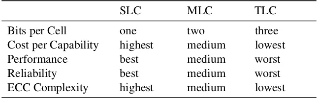
Table 1.1 NAND Characteristics
SLC MLC TLC
Bits per Cell one two three
Cost per Capability highest medium lowest
Performance best medium worst
Reliability best medium worst
ECC Complexity highest medium lowest
for its inherent weaknesses and has become an indispensable part of NAND flash memory
systems. In the era of SLC, the simple Hamming code is used frequently although it can
correct a limited number of errors only. For MLCs equipped in most NAND applications
today, the Reed-Solomon (RS) codes and Bose-Chaudhuri-Hocquenghem (BCH) codes
are being used to achieve better performance. All these ECCs are based on hard decisions
making their error correction capability limited in general. Due to continuous advances
in technology scaling and the fact that more bits will be added to each memory cell,
data reliability will get even worse in the future solid state memories. Therefore, more
advanced error correction codes based on soft decisions, such as turbo codes or low
density parity check (LDPC) codes will be the popular ECC algorithms used for future
NAND flash systems. The advanced error correction schemes can usually provide higher
error correction ability but result in higher software or hardware design complexity.
Table 1.1 illustrates the ECC requirements of NAND flash in different densities.
Among several soft-decision ECC algorithms, the LDPC codes are very promising
because of their capacity-approaching ability in the additive white Gaussian noise
(AWGN) channel. Additionally, the codes can be implemented with parallel decoding
schemes to achieve high throughput. All these excellent features have made the
LDPC-NAND a hot topic in the area of flash coding, and researchers are interested in removing
any obstacles that may prohibit the application of LDPC coding. Generally speaking,
there are three main challenges to adopting LDPC codes in SSDs, which includes
designing LDPC codes of good performance, exploring approaches to address the LDPC
decoder input initialization problem, and minimizing read latency induced by LDPC
structures for the same size LDPC may lead to very different performance. The good
candidates for error correction of NAND flash memory should achieve a low error floor
and fast convergence speed. Meanwhile, for additional improvement in error-correcting
performance, it would be a plus for the codes to contain the redundant parity checks.
Those prerequisites make the construction of LDPC codes for NAND flash channel more
complicated than the similar case for digital communication channels.
Secondly, the NAND flash memories provide hard decisions only due to the intrinsic
characteristics of the sensing circuits that decide the original bits during reading process.
While the LDPC decoder requires to be initialized with soft inputs, more efficient ways
have to be developed to get the required initialization values [30]. This has actually
become a critical issue recently for the LDPC-NAND error correction applications.
On the one hand, the flash channel is not easy to be precisely modelled. Simple
Gaussian models are usually adopted for flash coding research but the channel noise
distribution is actually far different from the Gaussian function. On the other hand,
non-uniform quantization can usually achieve more fine-grained soft-decisions than
traditional uniform quantization, however, it is difficult to find a good quantization
scheme in the unknown flash channel.
The third challenge is the read latency caused by the LDPC decoder circuitry [76].
To obtain the soft decisions for LDPC codes, multiple-precision sensing should be used
but it results in significant data access latency overhead. The read latency dramatically
limits the throughput of storage systems and becomes critical today as the data speed
of storage interfaces is getting faster and faster. For example, the Universal Serial Bus
(USB) 3.0, a commonly used interface for storage systems today, is over ten times faster
than the USB 2.0 used in the past.
This work is motivated by the problems discussed above. We wish to investigate
NAND flash channel, the flash error correction coding, and the flash memory controller
from the physical perspective. We propose and investigate efficient solutions to those
1.2
Goals
All throughout this thesis, the main intention is to improve the data reliability of NAND
flash memories. To this end, based on the discussions above, we shall focus the research
work on two topics: the data pattern processing and error correction. The problems
related to the topics will be investigated from the intrinsics of NAND flash memories, and
we aim to propose solutions based on the behaviours of the memory channel. Hardware
complexity will be considered as well since both the processing unit and ECC module
are implemented in flash controller in practice. The research goals set up for the doctoral
projects are listed below.
1. The first goal is to explore the physical connections between data patterns and
the flash read bit errors. The error probabilities based on different data patterns
shall be quantitatively analysed through either software or hardware simulation.
Based on discovered results, it is expected to propose a hardware-oriented write
pattern processing algorithm to improve the data reliability of MLC flash
memo-ries. Ideally, the proposed algorithm shall exhibit better performance and lower
complexity over the existing work in this direction. It is also preferable that the
proposed algorithm is designed without facing too many implementation issues in
the current practice.
2. In addition to the write pattern processing, this thesis also targets error correction
in flash memories. With respect to ECCs, the second research goal is set in the
dissertation to discover ways of extracting the soft information from the hard
decisions output of MLC flash memory. The performance of the classic multiple
reads method shall be evaluated by simulating a number of different reads over
MLC flash memories, and the disadvantages can be pointed out quantitatively.
Based on the experimental results, and the application background of LDPC
coding, it is expected to propose an error correction scheme that issues a novel
soft extraction algorithm and employs LDPC codes. The presented scheme shall
mechanisms. In the meantime, it is also expected that the soft extraction methods
shall be easy to implement and not induce much overhead in the sensing circuits.
3. This thesis aims to find an efficient way to quantize the sensing outputs for the
memory reads. Both the uniform and non-uniform sensing quantization schemes
will be investigated and simulated using the flash memory access model. The read
latency and complexity for different quantizations are compared, and the critical
factor influencing the performance shall be figured out. In the end, it is expected
to discover an optimized sensing quantization scheme that results in lower read
latency and can be applied in flash memory with the proposed ECC scheme to
achieve good performance.
4. The final goal is to characterize the flash memory channel and build a channel
model that fits the real situation as much as possible. Various existing channel
models are based on different kinds of approximation, while this thesis is trying
to propose a model without using too much approximation. All channel sources
of noise, distortion and interference shall be taken into account when calculating
the channel distribution, and it is expected to present accurate probability density
functions for the channel noise and final threshold voltage of each programming
level. Based on the results, future research may find out better solutions for
extracting soft information. Therefore it is of major importance for the future
research in flash coding.
1.3
Thesis Contribution
Several approaches have been used in this work to meet the research goals. The first way
is to investigate the storage systems and digital communication systems and compare
both from the intrinsic view. Keeping the differences in mind, some techniques used in
communication systems can be applied to flash memory and achieve remarkable
perfor-mance, provided only that the techniques be modified properly to fit in the application.
using the characteristic function of random variables is used in this thesis. Based on the
approaches and experimental results, this dissertation creates a channel model for NAND
flash memory and develops efficient fault tolerant solutions to improve the reliability
of flash-based data storage. The main contributions of this thesis are summarized as
follows.
1. This dissertation studied the practical low-complexity schemes that deal with data
pattern processing. A write pattern formatting algorithm (WPFA) is presented
to eliminate column stripe patterns and reduce the proportion of flash cells on
high threshold-voltage levels. The WPFA improves data reliability and relieves
the power pressure of flash memory effectively. With the proposed scheme, SSD
systems consume low energy and avoid suffering huge current spike. Compared to
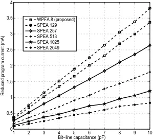
the current design practice that employs asymmetric coding and stripe elimination
algorithm (SPEA), the proposed algorithm consumes less overhead of NAND cell
area and exhibits better performance on power consumption. Associated hardware
design issues are considered with the aim of reducing complexity and utilizing
less logic resources. The advantages of the proposed scheme have been evaluated
by various metrics using both computer simulations and FPGA implementation.
Due to all these benefits, the proposed algorithm will be an attractive solution for
practical low-complexity data pattern processing schemes of SSDs.
2. As for the flash controller, the ECC module comes after the data pattern processing
scheme. Following the WPFA algorithm, this dissertation designed a novel fault
tolerant solution for flash memory that concatenates trellis coded modulation
(TCM) with an outer LDPC code. The concatenated TCM-LDPC fulfilled the
error correction capability of LDPC coding to achieve reliable storage in
multi-level flash. Moreover, the error correction performance is further improved since
TCM can decrease the raw error rate of MLC and hence relieve the burden of outer
LDPC code. Compared to the flash coding system that provides hard-decisions
and employs Bose-Chaudhuri-Hocquenghem (BCH) codes only, results show
LDPC codes and pragmatic TCM. This dissertation has also derived mathematical
formulations to quantitatively analyse the asymmetric coding gain achieved in
flash channels.
3. Another contribution that comes with the TCM-LDPC is the way it used to get
the soft values. Thanks to the Bahl, Cocke, Jelinek, and Raviv (BCJR) algorithm,
the TCM decoder can extract soft information from the hard-decision outputs of
flash read circuits. Such approach will not influence the sensing circuits, and thus
introduces less read latency than the classic multiple reads method. Given the
soft initialization values, the decoding of LDPC codes is feasible; as a result, the
BCJR and TCM will be a useful alternative in practice to extract flash memory
soft information.
4. Based on the study of BCJR for flash LDPC-TCM, this dissertation continues to
explore the ways of extracting soft information by investigating the flash memory
channel. The threshold voltage distribution after ideal programming in flash
memory cells is usually distorted by a combination of the random telegraph noise
(RTN), cell-to-cell Interference (CCI), and the retention process. This research
aims to characterize these various sources of distortion occurring in multi-level
cell (MLC) flash memories. The first contribution of this work is a mathematical
description of the overall distribution for the total flash channel distortion. The
final threshold voltage distribution for each symbol stored in MLC flash is also
formulated by using characteristic functions for the various sources of noise. With
the final cell threshold-voltage distribution, the soft information for each bit in the
cell can be calculated and applied for decoding soft decision-based error correction
codes. The results presented here are novel in a theoretical way as the first time
the flash channel has been characterized by incorporating the distributions of all
sources of interference and noise. Using the 4-level MLC flash as a case study, the
derived threshold voltage distributions and the results of the theoretical analysis
Chapter 1
Chapter 3
Chapter 4
Chapter 5
Chapter 6 Chapter 2
top level
physical level
Fig. 1.1 Overview of the thesis organization.
1.4
Thesis Outline
The overall structure of this dissertation is shown in Figure 1.1. Chapter 2 provides a
comprehensive background for the research topics investigated in the following chapters,
and elaborates on the nature of the reliability issues based on a literature review. Chapter
3, 4 and 5 study the research problem from different angles and present the corresponding
solutions or theoretical discoveries for each topic. The basic approach is to explore
the problem from the top level to the physical level of memory systems, pushing the
research deeper into the essential part of NAND flash. Chapter 6 briefly concludes the
dissertation.
The rest of the dissertation is organized as follows. Chapter 2 introduces the basics
of NAND flash memories. The reliability problem is brought out from the structure
and application background of flash memory and explained clearly based on the open
literature.
In chapter 3, we classify the errors in NAND flash memory into data retention
errors and program disturb errors, and focus on the data retention problem by assuming
that the program disturb has been alleviated in the sub-40 nm flash memory design.
Furthermore, we examine retention issue from the top level of memory system, i.e., the
data pattern processing module which is designed before the ECC and programming
retention process. Based on the measurement results and other scholars’ discoveries in
this direction, we present a novel write pattern formatting algorithm (WPFA) for MLC
flash memory to deal with data pattern processing. Comprehensive simulations and
implementation circuitry are also presented in this chapter. Additionally, the performance
and hardware complexity of WPFA are evaluated and compared with the existing work.
Chapter 4 shifts the study of the reliability problem to the lower level of flash
memory, the error correction coding, which deals with all kinds of errors. The
hard-decision based codes are popular in the current design practice. We investigate the
way of using the soft-decision based flash coding schemes that are capable to provide
better error correction performance. In chapter 4, we propose a combined TCM-LDPC
coding scheme for the error correction of MLC flash memories. The theoretical analysis,
computer simulations and performance comparisons are presented in this chapter as well.
For the further works of TCM-LDPC, we also discuss the approaches for soft-decision
extraction and sensing quantization.
Chapter 5 further investigate the application of advanced ECC from the physical
level and model the distribution distortion of flash memory channel. The noise and
interference are characterized and a mathematical description of all the sources of
distortion is presented in this chapter. Using the formularized expressions of noise
distributions, we further derive the final threshold-voltage distribution for each level of
MLC. The results are used to instruct the use of calculating soft decisions and applying
soft-decision based error correction codes.
Chapter 6 provides conclusions of the key results and insights presented in this
dissertation. Suggestions on how to use quantization, LDPC codes and other techniques
for future NAND flash memories based on the proposed flash channel model are also
Background
The aim of this chapter is to provide descriptions of the state-of-the-art NAND flash
technology. The NAND architecture and memory organization are reviewed first. Next,
an overview of NAND data reliability issues is presented, devoting particular attention
to the flash channel noise sources and error correction because they are necessary
prerequisites for the following chapters.
2.1
Basics of NAND Flash Memory
As a type of non-volatile storage, the NAND flash memory is able to keep the data
even when the power supply is switched off in the device. Due to this characteristic
the NAND flash memories have been used in storage products including compact flash
cards, solid state disk drives, flash memory dongles, and the image storage in digital
videos and cameras. The first NAND flash memory was invented in 1989 by Toshiba,
which surpassed previous types of non-volatile memory in terms of both capacity and
cost. During 1990s, the technology advances in the portable devices that use a battery
as power supply, including PDAs, mobile devices and digital storage, dramatically
2.1.1
NAND Device Organization
Depending on the manufacturer, there is some variation in the implementation of NAND
flash devices, resulting in two interface standards: Toggle NAND and Open NAND Flash
Interface (ONFI) NAND. Samsung and Toshiba make Toggle NAND, whereas virtually
everyone else makes ONFI NAND, including Intel, Micron, etc. These two standards
support different bus operations but have similar device organization. Generally speaking,
a NAND flash device is composed of one or more targets which is accessed through
an enable pad equipped in the memory chip. Die is the unit of a NAND flash memory
target, and one target is usually composed of one or more dies. The ONFI specification
also uses the name of logical unit (LUN) to represent the flash die, implicating that it is
the minimum unit that can execute commands and transfer data independently. Each
flash die is partitioned into multiple planes and a plane is further divided into blocks. For
the NAND flash device, block is an important which is the unit for erase and consists of
a number of pages for programming.
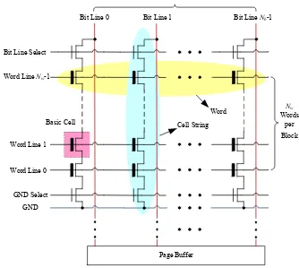
From the perspective of circuitry, the NAND flash block is a memory array that
consists ofNbbit lines (BLs) andNwword lines (WLs), as shown in Figure 2.1. The
memory cell string is the minimum array element which has 16 to 64 flash cells in typical
organization. Each block of the NAND flash memory contains a number of pages, for
example, the Micron 2Gb asynchronous SLC device is organized as 2048 blocks, with
64 pages per block. As for the erase operation, all the memory cells residing in the same
block shall be executed simultaneously, however, the read and program operations are
executed in the unit of page all the cells residing in the target page are written and sensed
at the same time. Each page has a data area and a spare area. The data area is used to
store the user data, and the spare area, also called the out-of-band (OOB) area, is used to
store the non-information data, such as the redundant bits for error correction code or the
flag bits for flash management algorithms. The bit-lines are shared by all memory blocks
in the devices, using an on-chip page buffers to hold the data for program and read. The
recent NAND Flash memories adopt either an interleaving bit-line architecture or all
Bit Line 0
Bit Line Select
GND
Basic Cell
GND Select
Page Buffer
Bit Line 1 Bit LineNb-1
Word Line 0 Word Line 1 Word LineNw-1
NbBits per Word (one or more pages)
Nw Words
per Block Cell String
[image:31.595.129.463.86.385.2]Word
Fig. 2.1 NAND flash memory array structure
not accessed at the same time but interleaved along the word line. This feature allow
each pair of even and odd bit lines to share the sense amplifiers and buffers, resulting in
less silicon cost of peripheral circuits. The situation is different for the ABL architecture,
where all the bit lines are accessed at the same time. The ABL NAND flash aims to
reduce the errors caused by cell-to-cell interference (as elaborated later in Section 2.2.2),
with a tradeoff to the peripheral-circuit silicon cost. Moreover, a current-sensing scheme
is required in the ABL structure, which is thought to be more complicated than the
voltage-sensing scheme used in the interleaving architecture.
2.1.2
NAND Cell Architecture and Basic Operations
NAND flash storage devices save data in a matrix of memory cells. Basically, the
memory cell has a built-in floating-gate MOSFET, which is also known as FGMOS. The
transistor in the flash cell is different from the standard four-terminal MOSFET with
N+ N+ Floating Gate
Control Gate Insulating
layer
Source
P-substrate
Channel
Drain
N+ N+
Control Gate
Insulating layer
Source
P-substrate
Channel
Drain
Flash Cell (FGMOS) MOSFET
Fig. 2.2 Flash memory cell vs. MOSFET.
on the technology today, even in the absence of a power input. Physically, the FGMOS
is originated from a standard MOS transistor but manufactured in a different way. It
has two gates: control gate and the floating gate, which are isolated electrically from
the body using an insulator likeSiO2. The control gate is placed above the floating gate,
which decide the threshold voltage of the flash cell by modifying the amount of charges
in the floating gate. There is no resistive connections between the control inputs and the
floating gate due to the fact that it is fully surrounded by the isolators.
Each NAND flash memory cell is configured to store the prepared information bits
by injecting a certain amount of charge into the floating gate. Usually Fowler-Nordheim
tunneling and hot-carrier injection mechanisms are used to modify the amount of charge
stored in the Floating Gate. The voltage level achieved by the amount of charge is
commonly called the threshold voltage of the NAND flash memory cell. The number of
electrons on the floating gate affects the threshold voltage, and the effect is measured
to determine the bits saved in the cell. Single-level cell (SLC) NAND flash has the
ability to store only one bit value per cell which therefore requires threshold voltage
level for each cell. The bit value is interpreted as either a “0” or a “1”. However, from
the perspective of developers, one of the major motivatives for NAND flash memory
development was to achieve maximum memory capacity and reduce the cost per bit.
Only after solving these two issues will the NAND flash devices be able to compete
with magnetic storage devices in the current market. Apparently, the SLC cannot fulfil
the requirements, therefore, the multi-level cell (MLC) flash was invented aiming to
values can be represented in an MLC flash cell, and the threshold voltage is used in the
same way as SLC to manipulate the multiple levels for the memory cell.
The basic operations on NAND flash include erasing, programming and reading,
all of which involve changes of cell threshold voltages. Unlike traditional hard disks,
a flash page has a write-once constraint because it can not be updated (or overwritten)
directly unless the page’s residing block is erased first. An erase operation involves
removing the charges before programming a memory cell, which sets the memory cell
threshold voltage to the lowest level. Comparing to the writing operation, the erasing
is completed in a way called tunnel release. Due to the inconsistency for the erase
operations, the threshold voltage of erased cells, denoted byVe, tends to reach a wide
normal distribution, which can be approximately modelled as
Ve=Vi(0)∼pe(x) =
1
σe
√
2π
e−(x−µe)2/2σe2 (2.1)
where µe and σe are the mean and standard deviation of the erased state. Here we
also useVi(0) to denote the threshold voltage of erased cells for the consistence of the
following discussions on NAND flash programming since the erased state is assumed as
the programming level 0.
For programming, a scheme called incremental stair pulse programming (ISPP),
or staircase algorithm, is utilized to reach a tight threshold voltage bound for the
representation of each symbol (or level) of the MLC. The ISPP scheme recursively
programs the memory cells on the same word-line through a program-and-verify method,
as shown in Figure 2.3. LetVpdenote the verify voltage of the target programmed level,
and∆Vppthe program step voltage. Ideally, the ISPP results in an uniform distribution
over the interval[Vp,Vp+∆Vpp]which has width of∆Vpp. SupposeVpandVp+∆Vppfor
thek-th programmed level are denoted asVl(k)andVr(k), respectively. Considering the
K-level MLC NAND flash for discussion, the threshold voltage of thekth programmed
∆Vpp Vp
time program verify
Fig. 2.3 Control-gate voltage in program operation.
Vi(k)∼p(pk)(x) =
1 ∆Vpp, V
(k)
l ≤x≤V
(k)
r
0, otherwise
(2.2)
To summarize, the initial cell threshold voltages ofK-level MLC flash memory,Vi(k)
for 0≤k≤K−1)have the following distributions
Vi(k)∼p(ik)(x) =
pe(x), k=0
p(pk)(x), 1≤k≤K−1
(2.3)
Note that the distributions in (2.3) are the ideal results for the programming of
NAND flash memories which, however, can be significantly distorted in practice by a
combination of noise and interference detailed in Section 2.2.2. Equipped with the ISPP
scheme, theK-level MLC NAND flash memory stores data by moving the threshold
voltage of each cell from the erase state to one ofKpredefined states that corresponds to
K non-overlapping windows. Ideally, the threshold voltages for cells written with the
samen-bit information shall fall into the same window, but the final threshold voltage
distribution could be distinct. The non-overlap space between the adjacent windows
is commonly called the distribution margin. For aK-level MLC NAND flash memory,
we use K−1 predefined read reference voltages to discriminate theK possible states
and make decisions on the final threshold voltage of each cell. TheseK−1 references
Erased State Programmed States
REF1 # cells
REF2 REF3
11 10 00 01
Vth
L0 L1 L2 L3
Fig. 2.4 Read reference voltages for 4-level MLC.
threshold voltage windows. Each threshold voltage window is determined by an upper
and a lower bound read reference voltage.
During a read operation, the cell’s threshold voltage is iteratively compared to
predefined read reference voltages until the upper and lower bound read reference
voltages are identified, thereby determining the stored bit value. The read reference
voltages and distribution margin for 4-level MLC are illustrated in Figure 2.4. In this
case we assume that the threshold voltages are not incurred with the flash channel noise,
thus the distributions resemble the ideal programming modelled in (2.3). Figure 2.4
shows that the cells in a given programmed state (e.g., L1 which indicates a logical bit
value of 10) have threshold voltages that fall into a distinct threshold voltage window
(e.g., threshold voltage values between REF1 and REF2).
In past flash generations, the read reference voltage values were fixed at uniform
intervals at design time. However, when the threshold voltage distributions are
dis-torted by multiple sources of noise and interference, the distributions can shift causing
distribution tails to enter the previously non-overlapping distribution margin regions,
crossing the read reference voltage levels. As a result, a cell that stored one logical
value can be misread as storing a different logical value, an event called a read error.
This is even more serious for MLC flash memories which have narrower distribution
margin than the SLC memories. One mechanism to combat such errors is called read
read reference voltages to be dynamically adjusted to track changes in distributions. The
basic idea is to retry the read with the adjusted reference levels such that read errors are
decreased or even eliminated. Another way is to use the non-uniform reference voltages
in the ECC decoder [16]. The non-uniform strategy senses the governing overlap region
with higher precision while leaving the other regions with lower sensing precision or
even no sensing. It reduces the sensing latency as well as read errors. The sensing
quantization is one of the important topics in the design of flash ECC schemes.
2.1.3
Planar and 3D NAND Flash Memory
Traditional planar NAND flash memory is classified as SLC or MLC flash memory.
Al-though MLC flash memory has worse read/write performance, reliability, and endurance
than SLC flash memory, it has gained the best market share because of its advantages in
cost and memory density. As predicted by the industry, flash memory is hard to scale
down below the 20 nm technology because too few electrons can be kept in the floating
gate of each cell, and each cell can not have a good margin to verify the voltage level.
In contrast, 3D NAND flash memory (also referred to as 3D flash memory) presents
a new trend in chip designs. Instead of simply shrinking the fabrication process and
flash memory cell size, a 3D flash memory chip applies single etching to punch through
multiple layers so as to create some shared hardware structure and reduce the bit cost.
Researchers and manufacturers are attempting to develop 3D flash memory because
3D flash memory is considered to be a promising way to continue to scale down
the die size and scale up the chip capacity. In the past few years, different types of
manufacturing technologies for 3D flash memory have been proposed. Bit-Cost Scalable
(BiCS) flash memory was first designed to share the process of bit line structures to
reduce the design cost. After BiCS, various types of structures were also proposed.
Well known examples are Pipe-shaped Bit-Cost Scalable (P-BiCS), Terabit Cell Array
Transistor (TCAT), Vertical-Stacked-Array-Transistor (VSAT), Dual Control Gate with
Surrounding Floating Gate (DC-SF), and Vertical Gate (VG). Among them, the VG
Layer 2
Layer 1
A B
C D
Fig. 2.5 A Typical structure of VG flash memory.
because of its scalability made possible by its small minimal cell size and well-controlled
interface. Figure 2.5 shows the structure of a two-layer VG flash memory. All of the
control gates of the cells from different layers but on the same vertical plane share the
same word line. For example, the control gates of cells A, B, C, D are connected to the
same word line because they are on the same vertical plane shown as a dotted rectangle
in Figure 2.5. When the number of layers increases, the structure can be easily extended
by connecting the control gates of the cells on the same vertical plane to the same word
line. These layers reside in the same flash memory chip thus increase the capacity of a
single chip significantly while keeping the similar die size.
In the past twenty years, the planar NAND technology has been developing to
approach its scaling limits, which poses grim challenges for the non-volatile memory
industry. In this circumstance the 3D NAND flash memory attempts to impress the
industry by keeping flash memory solutions consistent with Moore’s Law, the
trajec-tory for the continued performance improvement and cost cutbacks, promoting more
widespread application of NAND flash storage. Many big storage companies including
Intel, Samsung, Micron, and Toshiba are developing their own product lines individually
for the 3D NAND based storage solutions and expect to market those products in the
2.2
Data Reliability Issues
The continuing demand for NAND flash storage on better performance and higher
mem-ory capability has forced the manufacturers to probe to the limitation of the present
tech-nology and to develop new solutions, from both the physical and structural views [42].
For this technological evolution, the storage reliability is one of the critical obstacles
because the customers wish to be assured not only when a new product is initiated
but also demonstrated for the whole life cycle. Particularly, the manufacturers must
guarantee the minimum number of program and erase operations and the ability to keep
the saved data unaltered for a long enough period.
In this section, the prominent factors affecting the reliability of the traditional
FGMOS based NAND flash memories will be addressed. We discuss the issues at a
general level first and then delve into the detailed mathematics for each type of noise.
The topics of NAND flash write endurance and wear levelling are also introduced in this
section.
2.2.1
Reliability at Physical Level
The notion of reliability for NAND flash memory refers mainly to the errors and
disturbances caused before reading from the flash channel. We have discussed the read
errors caused by the narrowing down of distribution margin, which is not considered
here as one of the channel errors. Generally speaking, the errors occurring during the
flash programming and data storage can be classified into two major types: the program
disturbance errors and the data retention errors. Essentially these two reliability issues
are caused by flash program/erase (P/E) cycling effects and bit-line capacitance effects.
The frequent program/erase cycling causes the charges trapped in the oxide and
interfaces, which damages the tunnel oxide of the floating gate transistors, resulting in
the the cell threshold voltages variation and shifts. Therefore, the noise margin of the
flash memory chips is gradually downgraded as the P/E cycles increase. To the threshold
voltage of a certain flash cell, the first kind of distortion developed over the P/E cycling
These incidents eventually develop the electronic burst noise, bringing threshold voltage
fluctuation directly to flash memory. Meanwhile, the recuperation of interface trapping
and detrapping also causes slow reduction to the cell threshold voltage, leading to the
data retention issue.
There are two types of capacitances discovered in the flash memory channel: one
capacitance resides in the floating gate transistor and the other is the inter bit-line
capacitance, as shown in Figure 2.6. When a voltage is added to the control gate, the
floating gate starts to accumulate electrons and drives the cell threshold voltage to a
certain level with the help of the first kind of capacitance. This includes the capacitance
between control gate and floating gate (CONO), the capacitance between floating gate
and source terminal (CS), the capacitance between floating gate and drain terminal (CD),
and the capacitance between floating gate and the P-substrate body (CB), as shown in
Figure 2.6(a). Without these capacitances it is impossible to program the NAND flash
memories.
The inter bit-line capacitances cause notable threshold voltage shift to the
pro-grammed cells, thereby further degrading reliability. These propro-grammed cells are called
victim cells because their threshold voltages will be raised as neighbouring cells are
programmed. The neighbouring cells are called interfering cells. In Figure 2.6, cell 1
is the victim cell supposing it was programmed ahead of the five neighbouring cells.
The two neighbouring cells on the same word line are assumed to cause equal effects
because they have the same coupling capacitance to the victim cell, which applies as
well to the two cells in the diagonal positions.
2.2.2
Noises in NAND Flash Memory
As discussed earlier, the threshold voltage distribution after ideal programming in NAND
flash memory cells is usually distorted by a combination of noise and interference,
which include the random telegraph noise (RTN), cell-to-cell interference (CCI), and the
1 2 3 4
BL(i-1) BL(i) BL(i+1)
WL(i+1)
WL(i)
4 3 4
2 1 2
N+ N+
Floating Gate Control Gate
P-substrate
CS CB CD
CONO
(a) (b)
Fig. 2.6 Capacitors involved in the NAND flash memory channel.
presented, based on the open literature. We also present simulation results for threshold
voltage distortion caused by the multiple sources of channel noise.
Random telegraph Noise
The random telegraph noise (RTN) phenomenon, also named in old fashion as burst
noise or popcorn noise, was firstly observed in electronic devices including bipolar
transistors and junction field effect transistors during the 1950s. Evidence for RTN in
MOSFET devices has been reported since the mid-1980s [11]. The basic concept of
RTN is based on a mechanism where the electrons capturing and emission by interfacial
traps changes with time constantsτcandτe, leading to the fluctuations of FGMOS drain
current and threshold voltage. The effects caused by RTN depend on the flash memory
P/E cycling number since the electrons capture and emission are developed over the
cycling process [42]. Denote the threshold voltage shifts caused by RTN by∆VRT N.
The probability density function of∆VRT N can be modeled as a symmetric exponential
function
∆VRT N ∼pr(x) =
1 2λre
−|x|/λr (2.4)
where the parameterλr scales with the P/E cycling numberN in an approximate
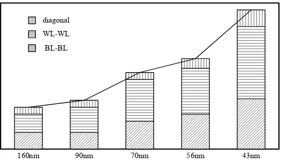
diagonal WL-WL BL-BL
[image:41.595.155.442.73.239.2]160nm 90nm 70nm 56nm 43nm
Fig. 2.7 Cell to cell coupling trend.
Cell-to-Cell Interference
In Section 2.2.1, we mentioned that the inter bit-line capacitances cause interference in
the flash memory channel and distortion of cell threshold voltages. This interference is
commonly known as the cell-to-cell interference (CCI) and has been recognized as the
major noise source in NAND flash devices. As the NAND flash technology keeps scaling
down, the neighbouring cells get closer and the inter bit-line capacitances between the
neighbouring flash cells become more and more notable, resulting in progressively severe
cell-to-cell interference and more serious distortion of threshold voltages. Conversely
speaking, the cell-to-cell interference is also a crucial barrier that holds back the future
NAND flash technology improvement. Figure 2.7 illustrates the trend of inter bit-line
capacitances versus technology scaling. Recall that the capacitances include three parts:
When the feature size of NAND flash memories reaches 4Xnm, where “4Xnm” means
that the design rule of the NAND flash device is restricted to the range of 40 to 50 nm, the
cell-to-cell coupling increases dramatically compared to old generations. Therefore, it
becomes very hard to achieve a tight distribution when using the staircase programming
algorithms in these feature-sized devices, making the real threshold voltage distributions
far different from the ideal programming.
The strength of cell-to-cell interference has been mathematically modelled by Lee
voltage shift of a victim cell caused by cell-to-cell interference, denoted∆VCCI, can be
estimated as
∆VCCI =
∑
lδV(l)γ(l) (2.5)
where δV(l) represents the threshold voltage shift of one interfering cell which is
programmed after the victim cell, andγ(l)is the coupling ratio subject to the parasitic
capacitance between the interfering cell and the victim cell. It is defined as
γ(l)= C
(l)
Ctotal (2.6)
whereC(l)is the parasitic capacitance between the interfering cell and the victim cell and
Ctotal is the total capacitance of the victim cell. Understandably, a memory cell would
be interfered only by the adjacent cells which are flashed after the write operations to
the victim cell. Due to the fact that the parasitic coupling capacitance decreases rapidly
with the distance to the victim cell increases, we only take the cell-to-cell interference
from the immediately neighbouring cells into account in the design practice.
The significance of CCI to a victim cell could be different depending on the NAND
flash architecture. For the interleaving architecture, cells on the even and odd bit lines
share one page buffer so they are programmed alternatively at different time. Since the
even cells are programmed ahead of the odd cells in the same word line, they are faced
with more cell-to-cell interference. With respect to one even cell, it sees interference
by five neighbouring cells: two adjacent odd cells, two diagonal cells on the next word
line, and one cell on the next word line and sharing the same bit line; all of which are
programmed after the even cell. On the other hand, the odd cell suffers interference
from three neighbouring cells only: two diagonal cells on the next word line, and one
cell on the next word line and sharing the same bit line.
For the all bit-line architecture, all the bit lines in the same word line share one page
buffer and are programmed at the same time. Therefore, all cells suffer the cell-to-cell