Abstract Compact and tunable semiconductor terahertz sources providing direct electrical control, efficient operation at room temperatures and device integration opportunities are of great interest at the present time. One of the most well-established techniques for terahertz generation utilises photoconductive antennas driven by ultrafast pulsed or dual-wavelength continuous wave laser systems, though some lim-itations, such as confined optical wavelength pumping range and thermal breakdown, still exist. The use of quantum dot-based semiconductor materials, having unique carrier dynamics and material properties, can help to overcome limitations and enable efficient optical-to-terahertz signal conversion at room temperatures. Here we discuss the construction of novel and versatile terahertz transceiver systems based on quantum dot semiconductor devices. Configurable, energy-dependent optical and electronic characteristics of quantum-dot-based semicon-ductors are described, and the resonant response to optical pump wavelength is revealed.Terahertz signal generation and detection at energies resonantly exciting only the implanted quantum dots opens the potential for using compact quantum dot-based semiconductor lasers as pump sources. A proof-of-concept experiments are demonstrated here and show quantum dot-based samples to have higher optical pump damage thresh-olds and carrier lifetime shortening trends with pump power increase.
1050 1100 1150 1200 1250
0 0.5 1
pump wavelength, nm
THz signal (a.u)
QD as emitter QD as detector
}}
QDQuantum Dot Materials for Terahertz Generation Applications
Ross R. Leyman
1, Andrei Gorodetsky
2,3,*, Natalia Bazieva
2, Gediminas Molis
4,
Ar ¯
unas Krotkus
5, Edmund Clarke
6and Edik U. Rafailov
2,3Introduction
Quantum dot (QD) materials were introduced around the same time [1] as the first generation of terahertz (THz) photoconductive antenna (PCA) devices [2]. QDs are often referred to as ‘designer atoms’ [3], because they can exhibit discrete energy levels and are highly configurable in their properties. The nano-scale size of the dots means that a sig-nificant degree of quantum confinement of charge carriers is exhibited in all three spatial dimensions, compared with a single dimension as in the case of semiconductor quantum wells (QW). Since then, QDs have been successfully imple-mented in many applications such as diode lasers [4–6], am-plifiers [7], saturable absorbers [8], photovoltaic devices [9] and biosensors [10]. All these applications take advantage of the distinctive properties of QDs, such as high thermal and optoelectronic efficiency and short charge carrier
life-time [11], properties that are also crucial for effective op-eration of photoconductive (PC) THz devices. Recently, re-search into efficient ultrafast PC materials and structures for THz [12–14] applications has included the investigation of optically-pumped QD-based semiconductor structures with the primary function of utilising layers of implanted QDs as the photocarrier lifetime shortening mechanism [4, 8]. This could potentially allow the production of a highly efficient, ultrafast device without introducing compromises between factors such as carrier mobility, PC gain, resistivity and carrier lifetimes as would normally be made in bulk-type PC THz materials. The use of essentially defect-free GaAs crystal layers in an InAs:GaAs QD structure allows carrier mobilities across the active region that are similar to low-defect density bulk semi-insulating (SI) GaAs structure and significantly higher than in a bulk low temperature-grown (LT)-GaAs [15].
1Institute of Photonics, University of Strathclyde, G1 1RD , Glasgow, UK
2Aston Institute of Photonic Technologies, Aston University, B4 7ET, Birmingham, UK 3ITMO University, St. Petersburg, 197101, Russia
4Teravil Ltd, LT-01108, Vilnius, Lithuania
5Center for Physical Science and Technology, LT-02300, Vilnius, Lithuania
6EPSRC National Centre for III-V Technologies, University of Sheffield, S1 3JD, Sheffield, UK
E
CBGS
ES E
ρ
GaAs substrate
}
QD
}DBR
1140 1200 1260 1320
0.2
0.4
0.6
0.8
1
Wavelength (nm)
DBR reflectivity
GaAs AlAs GaAs GaAsAlAs
InAs QD TEM image
pump laser lens
antenna
bias
Si lens
THz
(a)(b)
(c)
(d)
[image:2.595.70.495.85.363.2](e)
Figure 1 (a) Structure of quantum dot photoconductive antenna, QD – active region with several layers of InAs quantum dots implanted into GaAs matrix, DBR – distributed Bragg reflector; (b) cross-section TEM measurement of an InAs QD; (c) quantum dot material density of states, ECB– bottom of the conduction band, GS and ES – ground and excited states energies correspondingly, red line shows material photoluminescence spectrum; (d) reflectivity and schematics of AlAs/GaAs distributed Bragg reflector used in the antenna; (e) schematic of THz generation in the PCA.
Additionally, the use of implanted QDs as the active PC medium within a GaAs host crystal could enables the efficient optical-to-THz signal conversion when such a struc-ture is pumped at lower optical energies, transparent to the GaAs host but resonantly exiting carriers to and from the InAs QD sites. This in turn would open the opportunity for the development of all-QD, integrated or even on-chip THz sources or transceiver systems.
QDs deposited within or over GaAs have been demon-strated to efficiently shorten photocarrier lifetimes and en-able the generation of THz signals when the structure is pumped by ultrafast optical pulses with wavelengths be-tween 800 nm and 895 nm [14], and these lifetimes are ap-proximately the same as in LT GaAs. Thus GaAs PC devices incorporating QDs may offer the advantageous operating characteristics of semi-insulating (SI) GaAs while maintain-ing operatmaintain-ing speeds comparable to LT-GaAs [16].
Photomixing operation of PCAs has been demonstrated using ErAs:GaAs nanoisland-based structures pumped at around 800 nmusing two Ti:Sapphire lasers [12]. By chang-ing such parameters as the QD size, QD composition, den-sity of dots and number of QD layers in the active volume, the optoelectronic properties of the overall structure, such as energy level structure and carrier lifetime(s), can be pre-defined over a wide range – thus allowing a configurable
”match” for various specific ultrafast and CW QD-based compact pump lasers that operate at wavelengths in the re-gion of 1 µm to 1.3 µm. Moreover, the parameters of QD PCAs and QD laser diodes (LDs) may be perfectly matched at the design stage, which could result in even more effec-tive THz generation from a compact or potentially even single-chip device.
QD Structures
In all cases, the QD layers were each capped by 4–5 nm In0.15Ga0.85As layer and separated by a 35–36 nm GaAs
spacer layer, giving a total active region depth between 1 µm and 1.7 µm comprising either twenty-five or forty 40 nm QD sections. A TEM image of a single QD is shown in Figure 1(b). Atomic force microscopy measurements of uncapped QD layers grown under similar conditions show a QD density of 3×1010cm−2per layer, similar to areal QD densities for typical QD lasers. Faster carrier capture in QD ensembles with increasing QD density, as evidenced by a faster rise time in time-resolved PL measurements, has been previously reported in ref. [17]. The structures are produced with InAs dot layer thickness of 2.3 monolayers, which is enough to support significant dot layer density without risking a high density of dislocations. An extra spacer layer of GaAs was grown under the active PC region on an AlAs/GaAs DBR of either 25 or 30 layers (Figure 1(a)). Structures were grown by Innolume GmbH, Germany, and by the EPSRC National Centre for III-V Technologies at the University of Sheffield, UK. Growth parameters for the QD layers were intentionally kept as similar as possible between structures.
Ideal QDs exhibit carrier confinement in all three di-mensions, thus discrete energy levels with distinguishable density of states (DOS) profiles for each energy level would be expected. However, in real QD structures the DOS at each energy level is smeared over a Gaussian-type distribution due to small variations of the deposited dot sizes (Figure 1(c)). The need for the DBR is two-fold: to reflect the pump beam thus reducing the IR power at the antenna output, and to allow possibility for full optical cavity-type optimisation of the structure. Typical DBR layouts and reflectivity of the samples used are shown in Figure 1(d).
Pumping such structures at different excitation energies may induce a range of photocurrent processes which occur over different timescales, depending upon:i)which layer or material is optically excited, ii) which layer/material charge carriers relax to andiii) the level of optical exci-tation applied [18]. In the case of THz antennas there is the additional factor of the electric field applied across the active region, which affects carrier drift velocities and their subsequent capture times [19]. Ultrafast carrier relax-ation has been demonstrated in QD-based semiconductor saturable absorber mirrors (SESAMs) pumped at longer wavelengths corresponding to absorption energies of the implanted QDs [8]. Differential reflection measurements on QD layers with∼100 nm vertical separation showed sub-ps carrier capture from bulk GaAs into the wetting layer and
∼1.5 ps capture time into the QDs [20]. Additionally, the periodicity of embedded QD layers has been shown to also strongly influence the carrier capture time [21].
Carrier interactions and transitions in low-bandgap QDs are due to both radiative and non-radiative recombination and relaxation processes. When pumped at the wavelengths around 800 nm (allowing excitation of the GaAs barrier lay-ers), radiative process timescales can range from several ps to hundreds of ps [22, 23]. These timescales are determined by generation and diffusion of carriers from the GaAs bar-rier layers into the QDs, simultaneous state-filling of QD
energy levels, and subsequent energy-dependent exciton re-combination. Importantly however, it is observed that an increasing optical pump power leads firstly to saturation of the dot ground state (GS) and subsequently of the higher energy states due to comparatively low degeneracy of the GS [24]. Photoluminescence recombination measurements indicate a shorter recombination time from the excited states (ES) as compared to the GS. Non-radiative relaxation pro-cesses that result from the Auger effect [25] and step-wise (”intra-dot”) relaxation of excitons through subsequent QD energy states are dependent on both the available intraband relaxation channels and phonon interactions [26]. The dif-ference between carrier capture and carrier relaxation in this case is defined by whether photocarriers are considered as mobile or not mobile. Intra-dot carrier processes may be investigated by resonant excitation of QD states. Crucially, it is observed that increasing optical pump power in this regime reduces carrier recombination times, and this pro-cess is temperature dependent [27], which emphasises the importance of Auger-based processes.
THz Generation in QD based devices
The operation of a PCA device is based on the generation of photocurrent and the movement of charge carriers, and as such their mobility within the structure and between gen-eration and capture sites is a prime concern. In addition to intra-dot processes, the nature of inter-dot (mobile) pro-cesses must be considered in the pumping of such structures at resonant QD energies. Such processes are governed by carrier escape from QD sites into the barrier layers, which is in part dependent on the relative band energy mismatch between the QDs and wetting and spacer materials and a po-tential tunnelling between them. Application of an electric field across the active QD layer region of an InAs:GaAs het-erostructure under IR excitation has been previously demon-strated to enhance the movement and subsequent capture rate of charge carriers [28] down to sub-ps times, which is not observed during excitation of an un-biased structure. This dependency of the carrier relaxation rate on the exter-nally applied electric field for ultrafast carrier relaxation is typically not present in more homogeneous, bulk semicon-ductors grown at low temperatures, which suggests that in QD-based structures a more complicated sequence of carrier capture and relaxation events is taking place.
1000 1050 1100 1150 1200 1250 1300 0
0.5 1
QD pump wavelength, nm
QD Emitter signal (a.u)
QD photoluminescence
QD as emitter
QD as detector
QD
GaBiAs
emitter
detector
L
M
M
M
p-InAs
detector
emitter
L
BS
(a)
(b)
GS
ES1
[image:4.595.63.275.81.365.2]ES2
QD
Figure 2 Pump wavelength dependency of QD material in gen-eration and detection regimes and its photoluminescence. (a) Setup layout, for both experiments, arrows depict the difference in THz propagation from corresponding sources to detectors; FL – femtosecond laser, OPO – optical parametric oscillator, BS – beamsplitter, M – mirrors, L – lenses; (b) wavelength dependen-cies of THz signals emitted by QD sample and registered by GaBiAs detector (blue) and emitted by InAs crystal surface and registered by QD detector (red), GS – ground state, ES1 – first excited state, ES2 – second excited state. Photoluminescence curve is inserted to show wavelengths corresponding to GS and ESs.
The experimental system for testing of the QD mate-rial spectral response required broad wavelength tunability, which was achieved by using an optical parametrical oscil-lator (OPO). An amplified Yb:KGW laser system (Light Conversion ”PHAROS”) operating at 1030 nm wavelength with a pulse duration of 160 fs and repetition rate of 200 kHz was the main optical pump source. This laser was also used to drive a cavity-tuned optical parametric oscillator (OPO, Light Conversion ”ORPHEUS”) generating 140–160 fs du-ration pulses with a peak wavelength tunable from 640 nm to 2600 nm, and the THz output signal was detected by a sample of pre-characterised LT-GaAsBi, which in turn was pumped using the Yb:KGW beam. A dipole antenna with a length of∼90 µm and a PC gap width of∼10 µm was in-tegrated with QD-based structures and tested for excitation wavelength susceptibility in both operation modes – with a QD-based antenna used as either the THz emitter or the THz detector. In the first case, (Figure 2(a), upper arrow), the antenna structure was pumped by an OPO that generated fs
pulses of different wavelengths, while generated THz radia-tion was coherently sampled by an LT-GaAsBi-based PCA detector. GaAs is effectively transparent at wavelengths roughly≥880 nm and any fraction of the long-wavelength pump IR radiation not absorbed by the QDs is reflected by the DBR placed immediately beneath the active multilayer volume. When used as a coherent THz detector, (Figure 2(a), lower reverse arrow), the photocurrent at the QD antenna was measured at different pump wavelengths, while sensing THz radiation generated by a p-InAs based source which was pumped by the non-converted 1030 nm–wavelength femtosecond laser radiation [29]. Measured dependences are presented in Figure 2(b). The wavelength dependencies of both QD THz emission obtained in the first experiment (blue) and QD detector antenna photoconductivity mea-sured in the second experiment (red) shows distinct peaks in the vicinity of the intra-dot electron transitions corre-sponding to the QDs first and second ES. Hence, QD based antennas may also be used in conjunction with semiconduc-tor laser pump sources in the 1100–1300 nm wavelength range. The key enabling concept here is the use of similar InAs:GaAs QD structures in both the laser pump source and photoconductive THz emitter, and the complimentary emis-sion and absorption energies exhibited by the InAs:GaAs laser and antenna, respectively. Additionally, efficient THz generation and detection under pump wavelengths shorter than ∼880 nm are due to carriers that were generated in the GaAs substrate and captured by the QDs, showing the possibility to pump with a Ti:Sapphire fs laser. The ”re-emergence” of efficient THz signal conversion as the pump energy approaches the corresponding excited-state levels of the implanted QDs is perhaps the most significant nov-elty demonstrated here. The time-domain analysis presented in this work also confirms ultrafast carrier recombination behaviour theoretically predicted earlier [30, 31], where, among other effects, increasingly shortened carrier recombi-nation times from higher-occupancy (excited-state) energy levels of implanted QDs with increasing carrier density, via phonon-assisted Auger interactions has been predicted. Also, slower GS recombination times can explain the ab-sence of THz signal at GS pump energies, where most pho-toluminescence, which is not as lifetime dependent occurs. For∼800 nm pump and coherent time-domain measure-ments we used a Ti:Sapphire ultrafast laser (Sprite, M2 Ltd.) (810 nm wavelength, 99.5 MHz repetition rate, 150 fs pulse duration and 320 mW average power) and LT-GaAs PCA detector provided by Teravil Ltd, Lithuania.
When pumping a QD PCA using a Ti:Sapphire laser that operates at wavelengths short enough to excite the bulk GaAs barrier layers, optical-to-THz signal conversion takes place and we firstly observe the typical quadratic increase in THz signal output power with increasing electric field applied to the PCA. However, at a certain value of antenna gap electric field strength, the THz signal starts to decrease. Interestingly, the point of signal saturation with respect to electric field strength appears to depend on the optical pump power, which is evident in Figure 3(b).
dependence Figure 3(c), with signal reduction occurring at lower fields applied under lower pump powers. This effect of electron velocity overshoot [32] is the additional proof of fast electron trapping by QDs.
Structures with fewer QD layers would saturate at lower PCA biases, due to the correspondingly lower number of dots and capture sites. As the pump power is increased, the corresponding saturation field strength appears to become higher. Bulk, low temperature-grown semiconductors typi-cally show the opposite behavior [33]. This difference in the saturation behaviour is mainly caused by different carrier
0 10 20 30 40 50
0 0.2 0.4 0.6 0.8 1
Laser pump (mW)
THz intensity (
µ
W)
27 kV/cm
20 kV/cm
13 kV/cm
10 kV/cm
3 kV/cm
0 5 10 15 20 25 30 35
0 0.2 0.4 0.6 0.8
Antenna field (kV/cm)
THz intensity (
µ
W)
50 mW
40 mW
30 mW
20 mW
10 mW
(a)
(b)
0 5 10 15 20 25 30 35
0 0.5 1
Antenna field (kV/cm)
Normalised THz signal (a.u.)
50 mW
40 mW
30 mW
20 mW
10 mW
[image:5.595.315.523.78.381.2](c)
Figure 3 THz generation from a 25 layer QD PCA pumped using a fs Ti:Sapphire laser: (a) THz power versus laser pump power, (b) THz power at different fields applied to antenna. (c) THz signal normalised to the pump power.
0 100 200 300 400
0 0.2 0.4 0.6 0.8
Pump laser energy density (
µJ/cm
2)
THz intensity (a.u.)
Stripline 40 V
Stripline 30 V
Dipole 20 V
Energy densitycorresponding to LT GaAs breakdown
intensity
0 20 40 60
0 1 2 3 4 5
Antenna bias (V)
Current (mA)
LT GaAs 35 mW pump
QD 800 nm 35 mW pump
QD 1157 nm 60 mW pump
QD Dark Current
(a)
[image:5.595.62.279.220.685.2](b)
Figure 4 (a) Photocurrents of LT-GaAs and 40 layer QD 50µm gap stripline antennas and dark current of QD antenna, (b) THz generation from a 40 layer QD PCA pumped using a fs Ti:Sapphire laser, THz power versus laser pump intensity. Dashed line shows breakdown energy density for LT-GaAs.
recombination routes in bulk and QD materials. In LT-GaAs, photoexcited electrons are captured by As-antisite defects – the main carrier recombination centres in this material – more than an order of magnitude faster than the photoex-cited holes [34], which leads to trap saturation. Conversely, electrons and holes captured by QDs at high excitation lev-els can recombine faster than at low excitations, due to the onset of stimulated transitions. The effect of carrier life-time shortening in QDs is similarly exhibited in QD-based SESAMs, where the increase in applied pump power tends to reduce carrier recombination times [8]. This, coupled with the high carrier mobility and comparatively high ther-mal conductivity of the InAs:GaAs structure, might explain this apparent demonstration of a THz PCA which operates more efficiently the more intensively it is pumped.
Discussion
Conventional LT-GaAs-based antennas with a similar elec-trode structure to the one used in this work (50 µm-wide separated coplanar striplines) usually allow a maximum laser pump power of up to around 50 mW1,2, which
cor-responds to intensity of∼2500 W/cm2or energy density of∼30 µJ/cm2for a typical Ti:Sapphire laser with a rep-etition rate of 82 MHz focussed into a 50 µm spot. QD-based devices tolerate much greater input intensity and respond superlinearly not only at lower pump powers (Fig-ure 3(a)), but also at intensities ten times greater than the breakdown threshold of a bulk LT-GaAs device (Figure 4(b)). QD antennas in this experiment were able to operate even when being pumped by over 300 mW average optical power focussed into 30 µm spot, thus giving the intensity of
∼45 000 W/cm2or energy density of∼450 µJ/cm2without any additional heatsink and no saturation in THz generation efficiency. Direct comparison of the generated THz power in these experiments reveals that conversion efficiency in QD PCA is for these samples 30 times less than in commercial LT-GaAs, however, taking into account the configurability of QD wafers, these values can be equalised in the future. For example, QD PCAs demonstrated much higher values of dark current than LT-GaAs, and this can be upgraded.
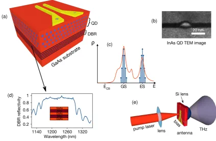
THz spectral broadening that can address carrier life-time shortening in QD wafers was also observed using both QD structures in a coherent time-domain detection regime. A Ti:Sapphire laser was used for pumping both the QD emitter and the LT-GaAs detector in these experi-ments. When changing the pump power within relatively low fluence limits, only the amplitude of the THz pulse is changed and, consequently, spectral features are kept con-stant, the THz signal being scaled evenly throughout the entire frequency spectrum (Figure 5 (c)). However, at higher pump powers, not only does the amplitude of the pulse in-crease, but the pulsewidth also decreases in time (Figure 5 (a), time-domain signals are shifted for readability). Trends for the points of THz pulse maximum amplitude and peak-to-peak duration are plotted in the inset of Figure 5 (b), and pulse shortening is clearly seen as well as pulse am-plitude growth. Thus, the corresponding spectra, shown in Figure 5 (b), reveal inhomogeneous amplitude growth, with the higher frequency range of the signal rising more than the lower at higher pump energy densities. THz amplitude spectra, normalised to one obtained at 20 µJ/cm2pump en-ergy density are shown in Figure 5(c)). They reveal rather homogenous amplitude growth at pump energy densities below 40 µJ/cm2and the rise of the higher frequency shoul-der starting from 60 µJ/cm2. Shortening of the produced THz pulse and resulting spectral broadening at higher pump powers could be explained by either Coulomb screening effect as described in [35] or by carrier lifetime shortening in QD samples due to Auger processes. Such carrier lifetime shortening mechanisms in the QD structure has also been
1 www.batop.com/products/terahertz/photoconductive-antenna/
photoconductive-terahertz-antenna.html
2 http://www.teravil.lt/emitter.php
−4 −2 0 2 4 6 8 10
−0.04 0 0.04
delay (ps)
THz signal (a.u.)
75 µJ/cm2
40 µJ/cm2
20 µJ/cm2
0.5 1 1.5
0.01 0.1 1
frequency (THz)
THz amplitude (a.u.)
75 µJ/cm2
40 µJ/cm2
20 µJ/cm2
0 25 50 75
0.8 1 1.2
pump (µJ/cm2)
Time (ps)
0.04 0.06 0.08 Amplitude (a.u.)
0.5 1 1.5
1 2 3 4
frequency (THz)
Normalised THz amplitude
75 µJ/cm2
50 µJ/cm2
40 µJ/cm2
30 µJ/cm2
(a)
(b)
[image:6.595.308.527.84.536.2](c)
Figure 5 THz signal generated in the QD PCA pumped with a Ti:Sapphire laser. (a) Time-domain profile of the main pulse at dif-ferent pump powers, (b) its corresponding amplitude spectra and (c) amplitude spectra normalised to one obtained at 20µJ/cm2. Insets show the antenna design (50µmgap stripline (a)) and de-pendence of THz pulse duration and amplitude on pump energy density (b).
reported earlier in similar structures [8], and were confirmed for our samples later [36].
0 10 20 30 40 50
100 150
Antenna bias (V)
THz power (pW)
30 mW QDLD pump
Log-periodic
electrodes
1160 1200 1240 0
5 10
wavelength (nm)
intensity (a.u.)
1 THz 1220 1230
λ
(nm)
E
1220 1230 λ
(nm)
E
Aspheric lenses
To antenna
QD Gain Chip
Di
ffraction
Grating
Di
ffraction
Grating
Beam dump
(a) [image:7.595.59.290.81.367.2](b)
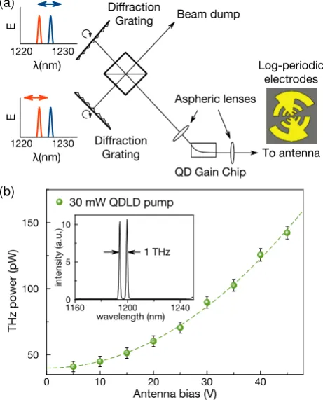
Figure 6 (a) QD LD in the double-Littrow configuration ; (b) CW THz intensity from 5µmgap log-periodic QD PCA pumped by this laser, measured by low-temperature bolometer. Dashed line shows quadratic fit. Inset: optical spectrum of the QD LD.
can be also tunable. One possible implementation of such a QD LD is the double-Littrow configuration [38] shown in Figure 6(a). Rotation of diffraction gratings allows simulta-neous and arbitrary tuning of both output wavelengths and thus the resultant THz difference frequency. An example THz output power trend from a 5 µm gap log-periodic PCA pumped by this laser tuned to 1 THz difference frequency is shown in Figure 6 (b). The antenna electrodes geome-try and pump laser optical spectrum that was used for this experiment are shown in the inset. The THz output power trend is repeatable and again is quadratically increasing with PCA bias. The highest conversion efficiency from this device was obtained while pumping the structure at wave-lengths between the peak energy level of the QDs 1st excited state and the photomixer cavity resonance peak at around 1220 nm. This also supports the previously demonstrated concept that the characteristic time of the fast component of carrier recovery in such InAs:GaAs QD heterostructures may be further reduced by excitation of the dots near the ES PL peak(s) [29]. No observable THz signals were generated when the PCA was pumped around the QD GS energy. The use of narrow-photogap interdigitated antenna electrodes together with higher pump powers from lasers operating at QD ES energies should allow higher PC gain and generated THz power.
Conclusion and outlook
A major motivation for the work presented in this paper is the development of an ultra-compact, efficient, room-temperature THz source or full measurement system and, ultimately, an elegant and complete THz transceiver or spec-troscopy system based on all-semiconductor elements in an ultra-compact housing.
The inclusion of multiple bandgap-engineered semicon-ductor materials and quantum-confined structures enables additional pump absorption energy ranges and ultrafast charge carrier dynamics, in principle slightly different to those of bulk semiconductors, which is important for the optimisation of pump-PCA interaction and may be partic-ularly crucial in the generation of continuous wave THz radiation. QD-based structures such as semiconductor lasers and SESAMs would normally benefit from optimisation of the monolithic optical cavity within the chip to enhance the interaction between either the pump or generated beam with the active medium, in this case the sequence of QD layers. The test structures used for this work were not optimised as such, and yet exhibited a optical-to-THz signal conversion factor comparable with that of state-of-the-art PCA devices. It is expected that a more tailored QD layer configuration, for example grown at depths corresponding to calculated cavity anti-node positions, could enhance the pump inten-sity, the carrier capture and interaction rate and hence the signal conversion process.
Low-defect absorption layers provide higher thermal conductivity and hence better pump power tolerance. Tun-ability of the photonic energies of QD LD output signals together with the versatile bandgap-engineering offered by QD-based PC materials, could allow the development of highly configurable, ultrafast optoelectronic systems. Both the LDs and the PCAs such as those used in this work may potentially be fabricated on the same epitaxial semiconduc-tor wafer and the implementation of QD-based lasers [4–6] as pump sources for QD-based antennas could eventually lead to fully QD-based integrated THz systems.
Acknowledgements.The authors thank D. Livshits from Innol-ume GmBH for providing samples and Richard Beanland from Integrity Scientific Ltd. for TEM image of a quantum dot. This work was supported by EPSRC Grant No EP/H015795/1 and FP7 IAPP TERA project No 285974, sample growth was funded by the NEXPRESSO program. A. G. Thanks Magicplot Ltd. for provid-ing a copy of Magicplot Pro plottprovid-ing and fittprovid-ing software used for preparation of all figures in the manuscript.
Key words: terahertz, photoconductive antenna, photomixer, quantum dots
References
[1] A. I. Ekimov, A. L. Efros, and A. A. Onushchenko, Solid State Comm.56, 921–924 (1985).
[2] D. H. Auston, K. P. Cheung, and P. R. Smith, Appl. Phys. Lett.45, 284–286 (1984).
[4] E. U. Rafailov, M. A. Cataluna, and W. Sibbett, Nat. Photon.
1, 395 – 401 (2007).
[5] R. Leyman, D. I. Nikitichev, N. Bazieva, and E. U. Rafailov, Appl. Phys. Lett.99(171107) (2011).
[6] K. Wilcox, M. Butkus, I. Farrer, D. A. Ritchie, A. Tropper, and E. U. Rafailov, Appl. Phys. Lett.94(251105) (2009). [7] E. U. Rafailov, P. Loza-Alvarez, W. Sibbett, G. S.
Sokolovskii, D. A. Livshits, A. E. Zhukov, and V. M. Usti-nov, IEEE Photon. Technol. Lett.15, 1023–1025 (2003). [8] E. U. Rafailov, S. J. White, A. A. Lagatsky, A. Miller,
W. Sibbett, D. A. Livshits, A. E. Zhukov, and V. M. Ustinov, IEEE Photon. Technol. Lett.16, 2439–2441 (2004). [9] R. D. Schaller and V. I. Klimov, Phys Rev. Lett.92, 186601
(2004).
[10] F. Tokumasu, R. M. Fairhurst, G. R. Ostera, N. J. Brittain, J. Hwang, T. E. Wellems, and J. A. Dvorak, J. Cell Sci.118, 1091–1098 (2005).
[11] P. Borri, S. Schneider, W. Langbein, and D. Bimberg, J. Opt. A.8, S33–S46 (2006).
[12] C. Kadow, A. W. Jackson, A. C. Gossard, J. E. Bowers, S. Matsuura, and G. A. Blake, Physica. E7(1-2), 97 (2000). [13] T. Kruczek, R. Leyman, D. Carnegie, N. Bazieva, G. Erbert, S. Schulz, C. Reardon, and E. U. Rafailov, Appl. Phys. Lett.
101(8), 0811144 (2012).
[14] E.Estacio, M. H. Pham, S. Takatori, M. Cadatal-Raduban, T. Nakazato, T. Shimizu, N. Sarukura, A. Somintac, M. De-fensor, F. C. B. Awitan, R. B. Jaculbia, A. Salvador, and A. Garcia, Appl. Phys. Lett.94(23), 232104 (2009). [15] D. Turchinovich, K. Pierz, and P. U. Jepsen, Phys. Stat.
Solid0(5), 1556–1559 (2003).
[16] A. Krotkus, J. Phys. D: Appl. Phys.43(273001) (2010). [17] S. Marcinkeviˇcius and R. Leon, Appl. Phys. Lett.76, 2406
(2000).
[18] H. P. Porte, P. U. Jepsen, N. Daghestani, E. U. Rafailov, and D. Turchinovich, Appl. Phys. Lett.94(26), 262104 (2009). [19] A. Lagatsky, E. Rafailov, W. Sibbett, D. Livshits, A. Zhukov, and V. Ustinov, Phot. Tech. Lett., IEEE17(2), 294–296 (2005).
[20] H. Y. Liu, Z. M. Meng, Q. F. Dai, L. J. Wu, Q. Guo, W. Hu, S. H. Liu, S. Lan, and T. Yang, J. Appl. Phys. 103(8), 083121 (2008).
[21] C. Kadow, S. B. Fleischer, J. P. Ibbetson, J. E. Bowers, A. C. Gossard, J. W. Dong, and C. J. Palmstrom, Appl. Phys. Lett.
75(22), 3548–3550 (1999).
[22] M. P. Lumb, E. Clarke, E. Harbord, P. Spencer, R. Murray, F. Masia, P. Borri, W. Langbein, C. Leburn, N. C. Jappy, Metzger, C. Brown, and W. Sibbett, Appl. Phys. Lett.95, 041101 (2009).
[23] K. Neudert, F. Trojnek, K. Kuldov, J. Oswald, A. Hospod-kov, and P. Mal, Phys. Stat. Solid6(4), 853–856 (2009). [24] R. Heitz, A. Kalburge, Q. Xie, M. Grundmann, P. Chen,
A. Hoffmann, and a. D. B. A Madhukar, Phys. Rev. B
57(15), 9050–9060 (1998).
[25] F. Adler, M. Geiger, A. Bauknecht, F. Scholz, H. Schweizer, M. Pilkuhn, B. Ohnesorge, and A. Forchel, J. Appl. Phys.
80(7), 4019–4026 (1996).
[26] J. Siegert, S. Marcinkeviˇcius, and Q. X. Zhao, Phys. Rev. B
72, 085316 (2005).
[27] T. Muller, F. F. Schrey, G. Strasser, and K. Unterrainer, Appl. Phys. Lett.83(17), 3572–3574 (2003).
[28] E. S. Moskalenko, M. Larsson, K. F. Karlsson, P. O. Holtz, B. Monemar, W. V. Schoenfeld, and P. M. Petroff, Nano Lett.7(1), 188–193 (2007).
[29] G. Molis, A. Arlauskas, A. Krotkus, R. Leyman, N. Bazieva, and E. Rafailov, in: 2012 37th Int. Conf. Infrared, Millime-ter, Terahertz Waves, (IEEE, 2012).
[30] A. L. Vartanian, A. L. Asatryan, K. A. Vardanyan, and A. A. Kirakosyan, Physica E42(4), 878–880 (2010).
[31] R. Ferreira and G. Bastard, Appl. Phys. Lett.74, 2818 (1999).
[32] A. Reklaitis, A. Krotkus, and G. Grigaliunaite, Semicon-ductor Science and Technology14(10), 945 (1999). [33] C. Ludwig and J. Kuhl., Appl. Phys. Lett.69(9), 1194
(1996).
[34] A. Krotkus, K. Bertulis, M. Kaminska, K. Korona, A. Wo-los, J. Siegert, S. Marcinkeviˇcius, J. F. Roux, and J. L. Coutaz, IEE Proc. - Optoelectronics, 149(3), 111–115 (2002).
[35] J. E. Pedersen, V. G. Lyssenko, J. M. Hvam, P. U. Jepsen, S. R. Keiding, C. B. Sorensen, and P. E. Lindelof, Appl. Phys. Lett.62(11), 1265 (1993).
[36] A. Gorodetsky, I. T. Leite, N. Bazieva, and E. U. Rafailov, in: CLEO EUROPE, (2015), p. CC 5 5.
[37] E. R. Brown, F. W. Smith, and K. a. McIntosh, J. Appl. Phys.
73(3), 1480–1484 (1993).