Abstract: Miniaturization and increased integrated system’s complexity in microelectronics have steered three-dimensional VLSI circuit design as a promising technological approach in the field of integrated circuit design. In recent times, three-dimensional integrated circuits (3D ICs) has evolved as an emerging technology that aids in overcoming the interconnect delay and power limitations of 2D ICs. This technology has become the center of attraction among the researchers and IC designers. The key idea behind this technique is to tightly integrate multiple silicon tiers using vertical 3D vias thereby reducing the interconnect length, resistance and capacitance that greatly influence the performance in terms of power and delay. Partitioning is the preliminary step in 3D IC design that maps the whole circuit into different design parts for allocation to different tiers. The current work develops a novel three-dimensional partitioner based on Cuckoo Search Meta-heuristic for partitioning and layer assignment of the netlist in 3D IC design, pertaining to a set of constraints such as inter-tier connections optimization and area balance. The proposed work is implemented on IBM benchmarks in MATLAB environment. The results highlighted reduced number of interconnect count and computational time for the proposed approach in comparison to the Meta –Genetic approach.
Index Terms: 3D Partitioner, Cuckoo Search, Layer Assignment, Wire-length Minimization
I. INTRODUCTION
At the age of nanotechnology, the demand for more compact devices increase day by day as many devices reduce to smaller size. Many of the electronic devices contain very large scale integrated (VLSI) chip responsible for the functioning of these devices. The information Technologies is demanding VLSI circuits with high functionality and performance at power dissipation and minimum cost. To meet this demand, VLSI circuits are scaled. However, due to large scaling of circuit some other issues come under the focus for semiconductor industry. For large size circuit, inter connection delays are increase and increasing in the interconnection loading influenced the consumption of power in high performance chips. In 2D VLSI chip, whole circuitry is laid on two dimensional silicon chip. Due to the demand of increase in functionality and good performance, the size of circuit expands. In 2D IC more functionality in chip requires more surface area. The Integrated circuit technologies are working on this area to overcome the problems faced in 2D IC
Revised Manuscript Received on June 11, 2019
Maninder Kaur, Computer Science and Engineering Department, Thapar Institute of Engineering and Technology, Patiala, India
Ashwin Prashar, Computer Science and Engineering Department, Thapar Institute of Engineering and Technology, Patiala, India
circuit technologies and to satisfy the some other constraints like area reduction, global wire length reduction, global delay etc. Additionally, scaling in inter-connect has significant effect on Computer Aided Design (CAD) methodologies and tools i.e. number of design cycles increases, and hence there is increment in the time and the cost per chip function. Integration of disparate signals like- digital, analog and technologies like- SOI, GaAs and so on is introducing for which existing two-dimensional (2D) technology may not be appropriate. The 2D system design cannot cater to the needs of more functionality in compact size thereby compelling the researchers to dig into the era of 3D-ICs. The 3D ICs offer an alluring substitute to the 2D ICs. In 3D VLSI chip design, many silicon chips are stacked one on other depend on numbers of tier required for any architecture. The stacking of 2D planar circuits forms 3D circuit. Three-Dimensional (3D) technique has abundant strength to increase the efficiency and ease of diversity of the IC
Three-dimensional (3D) integrated circuit (IC) is a providing better solution to the new generation of electronic designs. In 2D technology all devices are arranged on the single chip whereas in 3D ICs multiple chips are stack one on other having smaller size as compared to the 2D ICs. Hence, in result, form factor of 3D ICs is reduced and packing of devices become closer. Due the compactness of 3D-IC, it helps in the reduction of interconnects and hence help to improves performance. Through 3D-ICs, the heterogeneous integration can be realized by fabricating chips having different functionality on single stack. With the help of Through Silicon Via (TSV), one can achieve inter layer communication throughout the chip stack. TSV is micro channel of metal passes vertically through the stack of chips by penetrating within silicon substrate. A TSV links net connecting different chip of 3D design, by placing it on any white space that can be viable on the chip. With the help of TSV there is significant reduction in signal delay and wire-length.
Through-silicon-via (TSV) is a way to establish the interconnection among the silicon chips arrange in several 3D integrated circuit designs. TVS-based physical 3D circuit design also helps to reduce the overall wire length and delay among the circuit elements. It also helps in the reduction of chip area. Although, 3D-via occupy more area on the chip as compared to other elements. Hence, there is need to minimize the number of TSVs when we are entering to 3D era.Hence, it becomes important technique for the 3D physical design of the circuit.
Three dimensional IC become the main attention topic since past few years
Partitioning in Three Dimensional Integration
Microelectronics using Cuckoo Search
Meta-heuristic
and has been observed for many perspectives like fabrication process [1], [2], cost of production [3], thermal issues [4] -[6]and yield rate [7]. In the initial research, it was found that there was significantly reduction in interconnections with the presence of vertical connections. A high density of inter-tier connections on the chip with TSVs can be incorporated but the area occupied by TSV on the chip cannot be ignored. However, in reality as the numbers of TSVs are increased, there is increase in size of chip and length of inter-connection. Hence, realization of large number of TSVs on the chips does not favor the better performance of the design. On the other hand, minimum number of TSVs unable to bring advantages incorporated by TSVs. Hence, to get complete benefit of TSVs for the 3D physical design of chip it is required to optimize the number of TSVs. M. Tsai [8] studied impact of number of TSVs and wire-length on the 3D-ICs. The work utilized the varying size of TSVs i.e. from 10μm to 200μm, thereby evaluating the optimum number of TSV that accounted for higher performance of the chip [9, 10]. Therefore, it is important to find out that how the designs of 3D-ICs are affected by different technologies of the TSVs.
Partitioning phase in physical design of circuit is a NP complete problem, since, as increase in size of circuit with respect to cells and nets its computational complexity increases exponentially [11]. In partitioning, a given circuit is divided into parts with minimum number of interconnection between different parts. In 2D partitioning, resultant parts are allocated on different block created on the chip. Whereas, in 3D partitioning resultant parts allocated to different tiers of the chip stack. Many simple and meta-heuristic methodologies are suggested to solve this partitioning problem in 2D integrated circuit with some considerable output but minimal work has been done in the field of 3D ICs. The paper presents a new algorithm based on cuckoo search technique for the partitioning of hyper-graph with the objective of minimizing 3D-via. Section 2 describes the literature survey on related work. Section 3 represents problem formulation. Section 4 states proposed algorithm for the partitioning of the 3D circuit. In section 5, the proposed work is tested against IBM benchmarks and the experiment results are shown. Finally, section 6 concluded the proposed work.
II. RELATEDWORKS
Since past few years, a number of authors dug into the algorithms related to three-dimensional (3D) physical VLSI circuit design. This section focuses on major variants involved in solving the problem of partitioning in three-dimensional integrated circuits.
Huang, Y. et al. [13] presented a layer aware iterative method named “iLap” for the minimization of TSVs in 3D structures. iLap applied on given netlist in bottom-up pattern, iteratively on each layer of the partition. Experimental results generated by iLap showed that number of TSV reduced by 35% as compared to other existing methods. Ghosal, P. et al. [14] presented a strategy for the partitioning of netlist with the constraints of minimization of inter-tier interconnections as well as area balancing. Inter-tier connections are implemented through TSV that occupy a lot of area. The authors assigned weight to every logical module according to the area occupied
with the assumption that each module had finite number of output lines. Sawicki, S. et al. [15] anticipated a new methodology for the partitioning of cells and I/O pads with the reduction in 3D vias and its effect. They presented two different strategies: one based on analysis of circuit structure and second based on minimization of number of inter connection between non-adjacent layers. Cheng Hu, Y. et al. [16] proposed multi-layer partitioner algorithm for 3D ICs. It is based on multi-level framework to partition the input netlist. On each level of partition, the partitioning method is applied during un-coarsening stage. The main aim of proposed work is to minimize the total number of TSV with the consideration of balancing the area of each layer. Area of circuitry elements and area of TSVs collectively form the total area of the chip. The proposed algorithm can be customized according to the 3D ICs structure. Chen, Y. et al. [17] proposed a two-phased layer aware algorithm for the partitioning the circuit with the objective of minimization of TSVs in 3D design. In first phase, OpenMP was applied to circuit to parallelise the bi partitioning with minimum numbers of cuts. In second, using simulated annealing method the result of first phase is improved. The proposed work reduced the TSV‟s numbers by 39% as compared to the existing methods. Tsai, M. et al. [8] presented a study on the number of varying size TSV and wire-length. TSV can help in the minimization of wire-length but it occupy more area on the chip area which impact negatively on the designing of the chip and cancel out the benefits brought by TSVs. Experimental results explained that maximum area occupied by TSV is 25.3% of the area occupied by cells. Beyond this, no wire-length reduction can be obtained. Ye, H.S. et al [18] presented an algorithm for the partitioning of an IC with the consideration of objectives to reduce the count of Through Silicon Via (TSV) as well as chip space. The main benefit of reducing the count of TSVs is not only the minimization in chip delay but also it helps to reduce the area of die. Proposed work partitioned the given circuit into sub-parts with minimum number of TSVs in short time. Lim, S.K. et al [19] presented many big challenges in the area of VLSI physical design for three- dimensional (3D) integrated circuits (ICs) containing Through Silicon Vias (TSVs). Several issues were centered on Through Silicon via (TSV), which were the new for the 3D IC design. The authors concluded that it is crucial to investigate the impact of through silicon via on the qualities of overall layout, i.e. manufacturability, performance, reliability and power. The authors [20] studied the optimal level of partitioning in three-dimensional design and correlated the MAX-CUT partitioning with 3D nets. The results concluded that a system with 2048 cluster count, the net cut count on average is 35% i.e. 73 % fraction of total wire length in 3D IC design.
Consider a random collection of logical circuit netlist and a targeted 3D architecture with fix space and fixed count of tiers. The problem relies on the assumption that the gates say from v1 to vn-1of the netlist have same weight and a node say
vnillustrates a collection of all I/O pads inthe circuitry under consideration, with vn placed at the bottom most layer. The problem of three- dimensional circuit partitioning can be expressed as follows:
Given a circuit netlist portrayed by a graph G (V, E) wherein the set V = {v1, v2, ., vn} depicts the n vertices/gates of the circuit and set E = {e1, e2,...em} illustrates m-hyperedges that make connection among circuit elements. . Let K is the number of tiers, such that K = 2l with l = 1, 2, 3,. so on. The problem of three dimensional partitioning relies on mapping the whole circuit netlist on K tiers except bottom most layer (reserved for I/O pads) based on the objective of minimizing inter-tier connections i.e. TSVs by generating partitions such that the total number of 3D-via count is minimized with the area balancing constraint
IV. PROPOSEDALGORITHM
The work presents a layer aware 3D partitioning method named Partitioner and Layer Assignment in 3D ICs using Cuckoo Search Meta-heuristic(PLAC) that utilizes the Cuckoo search algorithm, a novel meta-heuristic nature-inspired optimization algorithm, proposed by Yang and Deb in 2009 [12]. The core Cuckoo Search (CS) approach is established on the parasitic behaviour of specific class of cuckoos that was formerly intended for solving continuous optimization problems. The underlying search strategy utilizes levy flights to perform random walk for improving solutions by speeding up the local search. The cuckoo algorithm does not trapped in a local optimum as the system produces some far field solutions. The basic units of the technique are as follows:
A. Solution Encoding
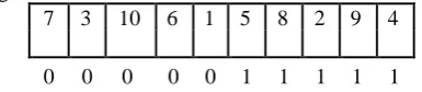
[image:3.595.319.543.256.425.2]A solution is represented as a ordered arrangement of circuit elements belonging to the input netlist file[21],with one egg/ cuckoo representing one solution that partition the given netlist into sub-parts. The array data structure contains a permutated sequence of cells and I/O pad with initial set of elements assigned to one partition (say 0th) and rest to other (i.e. 1st), satisfying the balanced constraints as illustrated in Figure 1.
7 3 10 6 1 5 8 2 9 4
0 0 0 0 0 1 1 1 1 1
The algorithm initiates with random population wherein the solutions reveals the current living position of all cuckoos by defining a matrix of size n X p with p
–population size and n is number of cells. Large circuit size
as in the existing set of IBM benchmark adds to space complexity. To reduce this space complexity, the proposed PLAC approach in its initial step stores only half of the total cell that belong to one partition and remaining half set of elements can be evaluated by using set theory operations using set difference operation i.e. universal set minus known half set.
B. Step size
The distance between best solution and newly generated solution, say mth and nth cuckoos, is represented by the term
step size (α). Through the step size, current generated solution moves towards the best solution if and only if the current solution is not better than existing best solution. It is calculated by counting the difference in the number of elements between any pair of partitions of different solutions.
mth cuckoo-
7 3 10 6 1 5 8 2 9 4
0 0 0 0 0 1 1 1 1 1
nth cuckoo-
Part 0 Part1
7 1 4 6 9 5 8 2 10 3 0 0 0 0 0 1 1 1 1 1
[image:3.595.56.249.582.624.2]Part 0 Part1 Fig. 2 Shows the two different solutions having 10 cells. For the solutions as given in figure 2, the distance between them is calculated in four ways.
Distance (mth part-0, nth part-0) = 2. Distance (mth part-0, nth part-1) = 3. Distance (mth part-1, nth part-0) = 3. Distance (mth part-1, nth part-1) = 2.
For the fast processing, the value of α having lesser distance between solutions is chosen i.e 2 (in this example) as the minimum distance between two cuckoos or solutions.
C. Updating the Solution
The current cuckoo solutions are modified using the step size α and the step length called Levy flight, drawn from Levi‟s distribution. Here, the value of Levy flight considered as one. The solution updating scheme can be formulated as in eq(1).
xj(i+1) = xj(i) + α = xj(i) + (xj(i) – xbest(i)) (1) (1)
.
Fig. 1 Solution encoding
PLAC ( File_IO , Num_gates, Num_nets, Pop_size, Num_of_gen, Pα , No_of_Layers,Vs)
Input: Read the Benchmark files in circuits
Output: Layered Partitions of all the movable objects in netlist
Begin
Set variable Layer = 1
Set variable K = Num_gates / No_of_Layers Initialize Vs: as a set of IO_PADS
Repeat for G Vs
Layer_Assignment(G):=0 EndFor
Netlist=CreateNetlist (File_IO, Num_gates, Num_nets) Repeat for L=1: No.of_Layers-1
(P1,P2)=Cuckoo_partitioner(Netlist,Num_gates,Num_nets,Pop_size,Num_of_gen,Pα,Vs,K)
Vs= Vs P1
Netlist=Netlist P1 Repeat for G P1 Layer_Assignment(g):=L
EndFor EndFor End
Cuckoo_partitioner (Netlist, Num_gates, Num_nets, Pop_size, Num_of_gen, Pα, Vs, K)
Input: pop_start, pop_update are structure array of size (Num_gates X Pop_size) pop_new is structure array of size (Num_gates X Pop_size-1)
best_pop is an individual of population of size (Num_gates) Output: Two Partitions A1 and A2 having min-cut
Begin
[pop_start] = initialise (Pop_size, Num_gates, Num_nets)
Find_Fitness (Netlist, pop_start, Num_gates, Num_nets, Pop_size, Vs, K)
Initialize iter: =1
Repeat while iter <= Num_of_gen
[best_pop] = Find_Best (pop_start, Pop_size, Num_gates, Num_nets) TR=Calculate_Threshold(best_pop, Pα )
Set j: = 1
For i =1 to Pop_size
If best_pop = pop_start(i) i=i+1;
Endif
Do
Step_size = Arc_diff (best_pop, pop_start(i), Num_gates) pop_new(j) = Levy_flight (pop_start(i), Num_gates, Step_size ) net_cut = Find_Fitness_Individual(pop_new(j), Num_gates, Num_nets) pop_new(j).fit = net_cut
While (pop_new(j).fit > TR ); Set j=j+1
Endfor
pop_update = Update_solution (Pop_size, pop_start, pop_new) pop_start = pop_update
iter = iter +1 Endwhile End
For the random walk around the best solution is done as in eq (2)
xj (i+1)
= xj (i)
+ εi (2) (2)
Here, εi represent a random value within the range of [0, n/2]
(where n is the count of cells plus one node for I/O pads) and the value of εi is generated from uniform distribution.
In Levy_flight, corresponding solution moved towards the best solution present currently with the step length of one, by considering step length equal to it helps in fast improvement in the solutions
D. Threshold calculation
The threshold value decides whether the newly generated solution should be accepted or not by comparing the fitness of the solution with threshold value. If the fitness of generated solution is more than threshold criteria, the solution is rejected.
The threshold value is calculated as given in eq(3)
Threshold value = fitnessbest_solution X [1+ .01 (1-Pα)] (3)
where fitnessbest_solution denotes the fitness value of best solution of that iteration and Pα. denotes the value of probability factor given by the user such Pα ϵ [0, 1]. Higher the value of Pα , greater will be chance of finding foreign egg by host bird leading to more chances of solution rejection according to their fitness value.
The PLAC approach is demonstrated by the pseudo code as given in figure 3. The approach is based on breadth first recursive layer-aware min cut partitioner that uses the underlying cuckoo search based partitioner. Firstly, each cuckoo generates an initial set of solutions/eggs of population size „n‟ randomly and finds the best nest based on min-cut objective function. After the evaluation of the initial population, the algorithm enters its main loop that is executed for a given number of generations. In each iteration, the existing solutions except the best solution, are further processed for next generation using the Levy flight towards the best solution. In this step Arc_diff is calculated for each solution to find the step size whose value is passed to Levy_flight() function. In Levy_flight, corresponding solution moves towards the best solution generating new solution if the fitness value of newly generated solution satisfies the proposed threshold criteria (eq. 3) then the new solution is accepted, otherwise the whole procedure is repeated to generate better solution until threshold criteria is satisfied. In the each generation, total„n‟ solutions are selected from newly generated „n-1‟ solutions and old „n‟ solutions (from previous generation) on the basis of their fitness value for the next iteration . The underlying cuckoo based layer aware partitioner generates two partitions having min-cut.Since PLAC approach continues till desired number of layers generated, Cuckoo_partitioner, is called recursively
until the desire number of partitions are produced using queue data structure.
Finally, when required sub-partitions for the number of layers are generated by the PLAC approach, the next step is to assign layers to all partitions one by one. Starting from the sub-partition having last node entry, assign this to the layer just above the layer containing all I/O pads (bottom most layer). After that sub-partition, just separated from the assigned sub-partition will be assigned to the layer above the previously assigned layer. This procedure will be followed until the all sub-partitions are assigned to all layers of 3D design, making layer aware partitioning PLAC approach help in reducing the number of 3D vias generated by the cell to I/O pads interconnections.
V. RESULTS&DISCUSSION
The proposed PLAC technique is executed on MATLAB (R2016a) on Intel core i7 processor, with 16 GB RAM and 64- bit Operating System. The work is applied on different circuits of IBM benchmarks [21] and the results are compared with the Meta-genetic approach. The description of IBM benchmark used is given in table 1.
Table 1. Characteristicsof IBM benchmarks used.
Benchmark Circuit Cells Nets I/O Pads
Ibm01 12506 14111 246
Ibm02 19342 19584 259
Ibm03 22853 27401 283
Ibm04 27220 31970 287
Ibm05 28146 28446 1201
Various control parameters used in PLAC approach are:
Pα-this factor is directly related to the acceptance and rejection of solution,
No_of_Layers- The high value of No_ of_ Layers
[image:5.595.337.520.576.628.2]more is the number of TSVs.
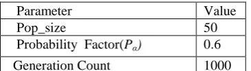
Table 2 presents the finalized values of parameters on the basis of the results from different runs. Increasing the values of parameters such as PoP_Size and Generation count beyond this range improves the chance of the algorithm in finding its optimal solution, yet, simultaneously it leads to substantial rise in computing time.
Table 2: DCS Parameters
Parameter Value
Pop_size 50
Probability Factor(Pα) 0.6
Generation Count 1000
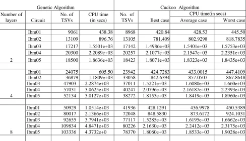
Table 3. Comparison of cuts and CPU time (in best, average and worst case) for proposedalgorithm and meta-genetic approach (pop_size is taken as 50).
Genetic Algorithm Cuckoo Algorithm
Number of
layers Circuit
No. of TSVs
CPU time (in secs)
No. of
TSVs Best case
CPU time(in secs)
Average case Worst case
2
Ibm01 9061 438.38 8968 420.84 428.53 445.50
Ibm02 13109 896.76 13105 781.409 802.9298 818.7835
Ibm03 17217 1.5501e+03 17142 1.4986e+03 1.5401e+03 1.5753e+03
Ibm04 20300 2.2089e+03 20257 2.1077e+03 2.1547e+03 2.2351e+03
Ibm05 18500 1.8636e+03 18423 1.8071e+03 1.8323e+03 1.8435e+03
4
Ibm01 24075 605.50 23942 424.7283 433.0015 447.4109
Ibm02 36879 1.1809e+03 33058 842.6394 857.0507 867.8648
Ibm03 47903 2.2874e+03 37011 1.5221e+03 1.6080e+03 1.660e+03
Ibm04 57031 3.0625e+03 40247 2.0796e+03 2.16187e+03 2.2393e+03
Ibm05 52134 3.0127e+03 38272 1.8153e+03 1.8419e+03 1.8960e+03
8
Ibm01 50929 1.0514e+03 41936 428.1291 436.9978 450.5389
Ibm02 80017 2.1366e+03 72048 848.5830 873.6172 924.1031
Ibm03 92655 3.7941e+03 77117 1.5285e+03 1.6195e+03 1.6662e+03
Ibm04 109834 4.8471e+03 80226 2.1630e+03 2.2412e+03 2.3175e+03
[image:6.595.67.513.223.603.2]Ibm05 103336 4.3732e+0 78370 1.8060e+03 1.8533e+03 1.9028e+03
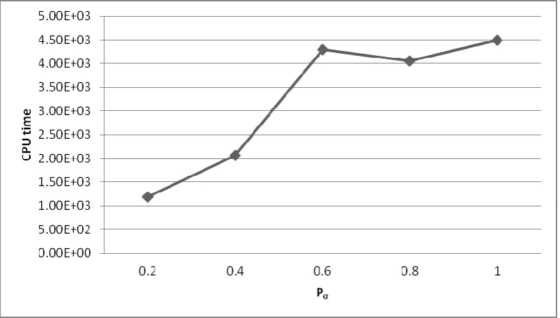
Fig. 5 Correlation between Pαand CPU time
There is an increase in the inter-tier cuts with increase in
[image:7.595.85.510.377.606.2]No.of Layers for different IBM benchmarks as depicted in Figure 4. The Figure 5 demonstrate the correlation between the probability of finding foreign egg (Pα) and required CPU
time to run at corresponding values of Pα. The PLAC
approach requires longer computational time and resources
when the value of Pα (Probability of finding foreign egg) is increased. This is because of the reason is that at high value of Pα there are more chances of rejection of worst solution. As a
result, there is a need of generating more solutions in the place of rejected ones.
Fig. 6 Comparison between number of TSVs generated by Cuckoo Search and GeneticAlgorithm for the 4 layer-partitioning.
Figure 6 shows the comparison of number of TSVs produced by both PLAC and Meta-Genetic Algorithm for partitioning the netlist in 4 tiers. It is clear from the figure that the PLAC
Fig. 7 shows the relation between number of TSVs and Number of layers. The relationship between no. of layers and no. of TSVs is
plotted in Figure 7. The figure shows that with increase in number of layers for the partitioning, the PLAC produces better optimization results than those obtained by Meta-genetic algorithm in terms of TSV count.
VI. CONCLUSION
Because of growth in the size of digital electronic circuit, 2D VLSI physical design process is moving towards 3D space. 3D technology helps to overcome the issues emerged under the 2D technology like increasing in the size of chip, uneasiness in the integration of heterogeneous technology, lager global wire-length, inefficient signal delay etc. In the current work, a cuckoo search meta-heuristic based approach named PLAC is proposed for partitioning the circuit netlist to be placed on 3D dice in a manner minimizing number of inter-partition connections (TSVs) while satisfying the area balance constraint. The PLAC approach is tested on standard netlist of IBM benchmarks and the results obtained are compared with the results from Meta-genetic approach. The comparison shows better performance of PLAC over Meta-genetic in terms of number of TSVs, CPU time, with the ability to generate good results for complex circuit design in acceptable CPU-time.
REFERENCES
1. P. S. Andry, et al., “A CMOS-compatible processor for fabricating electrical through-vias in silicon”, Proceedings of the 56th Electronic Component and Technology Conference, San Diego, 2006, pp. 831-837.
2. S. Spiesshoefer, Z. Rahman, G. Vangara, S. Polamreddy, S. Burkett, L. Schaper, “Process Integration for Through-Silicon Vias”, Journal of Vacuum Science and Technology A, vol 23, pp. 824-829, 2005. 3. K. Takahashi, M. Sekiguchi, “Through Silicon Via and 3-D
Wafer/Chip Stacking Technology”, Symposium on VLSI Circuit Digest of Technical Papers, 2006, pp. 89-92.
4. Zhou, Pingqiang, et al. "3D-STAF: scalable temperature and leakage aware floorplanning for three-dimensional integrated circuits." Proceedings of the 2007 IEEE/ACM international conference on Computer-aided design. IEEE Press, 2007.
5. Loi, Igor, Subhasish Mitra, Thomas H. Lee, Shinobu Fujita, and Luca Benini. "A low-overhead fault tolerance scheme for TSV-based 3D
6. Cong, Jason, Jie Wei, and Yan Zhang. "A thermal-driven floorplanning algorithm for 3D ICs." In Proceedings of the 2004 IEEE/ACM International conference on Computer-aided design, pp. 306-313. IEEE Computer Society, 2004.
7. Li, Zhuoyuan, Xianlong Hong, Qiang Zhou, Shan Zeng, Jinian Bian, Hannah Yang, Vijay Pitchumani, and Chung-Kuan Cheng. "Integrating dynamic thermal via planning with 3D floorplanning algorithm." In Proceedings of the 2006 international symposium on Physical design, pp. 178-185. ACM, 2006.
8. Tsai, Ming-Chao, and TingTing Hwang. "A study on the trade-off among wirelength, number of TSV and placement with different size of TSV." In Proceedings of 2011 International Symposium on VLSI Design, Automation and Test, pp. 1-4. IEEE, 2011.
9. Pathak, Mohit, Young-Joon Lee, Thomas Moon, and Sung Kyu Lim. "Through-silicon-via management during 3D physical design: When to add and how many?." In Proceedings of the International Conference on Computer-Aided Design, pp. 387-394. IEEE Press, 2010.
10. Banerjee, Kaustav, Shukri J. Souri, Pawan Kapur, and Krishna C. Saraswat. "3-D ICs: A novel chip design for improving deep-submicrometer interconnect performance and systems-on-chip integration." Proceedings of the IEEE 89, no. 5 (2001): 602-633. 11. Sait, SM, Youssef, H. VLSI Physical Design Automation: Theory and
Practice, McGraw-Hill, 1995.
12. Yang, X., Deb, S. Cuckoo Search via Levy Flights. In World Congress on Nature & Biologically Inspired Computing, 2009, pp. 210–214. 13. Huang, Ya-Shih, Yang-Hsiang Liu, and Juinn-Dar Huang. "Layer-aware
design partitioning for vertical interconnect minimization." 2011 IEEE Computer Society Annual Symposium on VLSI. IEEE, 2011.
14. P. Ghosal, S. Chatterjee, “Partitioning in 3D ICs: A TSV aware strategy with area balancing”, in International Conference on Devices, Circuit and Systems (ICDCS), Coimbatore, 2012, pp. 576-580.
15. S. Sawicki, G. Wilke, M. Johann, R. Reis, “3D-Via Driven Partitioning for 3D VLSI Integrated Circuits”, in CLEI Electronic Journal, vol 13, 2010.
16. Y.C. Hu, Y.L. Chung, M.C. Chi, “A multilevel multilayer partitioning algorithm for three dimensional integrated circuits”, in 11th International Symposium on Quality ElectronicDesign (ISQED), San Jose, 2010, pp. 483-487.
17. Chen, Y.H., Chen, Y.T., Huang, J.D. Parallel Layer-Aware Partitioning for 3D Designs. In SASIMI 2013 Proceedings, 2013, pp.176-179. 18. Ye, Hua-Sin, Mely Chen Chi, and Shih-Hsu Huang. "A design
partitioning algorithm for three dimensional integrated circuits." In 2010 International Symposium on Computer, Communication, Control and Automation (3CA), vol. 1, pp. 229-232. IEEE, 2010. 19. S.K. Lim, “TSV-based 3D Physical Design Tool Needs for Faster
Mainstream Acceptance of 3D ICs”, in Proc. 47thACM/IEEE DAC Knowl. Center Article, 2010, pp. 1-11.
International Symposium on Circuits and Systems. 2019.
21. N. Viswanathan, C. C. N. Chu., “ISPD04 IBM Standard Cell Benchmarks with Pads”,2004.
AUTHORSPROFILE
Maninder Kaur is holding an academic position as Assistant Professor in Department of Computer Science and Engineering, Thapar Institute of Engineering & Technology, Patiala. She received her Bachelor Degree from Sant Longowal Institute of Engineering and Technology and Master‟s degree from Punjabi University. She completed her Ph.D. in the field of VLSI physical design automation using Evolutionary approach. Her major research experiences and interests include IOT, Big Data Analytics, Data Mining and Swarm intelligence. She has 25 publications including prominent journals, conferences. She has also acted as mentor in various capstone projects in the field of IOT and machine learning. She is currently supervising two Ph.D. and two M.E. students. She has also supervised more than 11 M.E./M.Tech. thesis. She is an associate member of The Institution of Engineers, India. Her current research includes the application of machine learning and swarm intelligence techniques for big data analytics, cyberbullying and sarcasm detection.