Active Optical Metasurfaces
Based on Defect-Engineered
Phase-Transition Materials
The Harvard community has made this
article openly available. Please share how
this access benefits you. Your story matters
Citation
Rensberg, Jura, Shuyan Zhang, You Zhou, Alexander S. McLeod,
Christian Schwarz, Michael Goldflam, Mengkun Liu, et al. 2016.
“Active Optical Metasurfaces Based on Defect-Engineered
Phase-Transition Materials.” Nano Letters 16 (2): 1050–55. https://
doi.org/10.1021/acs.nanolett.5b04122.
Citable link
http://nrs.harvard.edu/urn-3:HUL.InstRepos:41371645
D. N. Basov,
§Federico Capasso,
‡Carsten Ronning,
†and Mikhail A. Kats
*
,‡,∇,○†Institute for Solid State Physics, Friedrich-Schiller-Universität Jena, 07743 Jena, Germany
‡John A. Paulson School of Engineering and Applied Sciences, Harvard University, Cambridge, Massachusetts 02138, United States §Department of Physics, University of California - San Diego, La Jolla, California 92093, United States
∥Department of Physics, Stony Brook University, Stony Brook, New York 11794, United States
⊥Institute of Ion Beam Physics and Materials Research, Helmholtz-Zentrum Dresden-Rossendorf, 01328 Dresden, Germany
#School of Materials Engineering, Purdue University, West Lafayette, Indiana 47907, United States
∇Department of Electrical and Computer Engineering and○Materials Science Program, University of Wisconsin - Madison, Madison,
Wisconsin 53706, United States
*
S Supporting InformationABSTRACT: Active, widely tunable optical materials have enabled rapid advances in photonics and optoelectronics, especially in the emerging field of meta-devices. Here, we demonstrate that spatially selective defect engineering on the nanometer scale can transform phase-transition materials into optical metasurfaces. Using ion irradiation through nanometer-scale masks, we selectively defect-engineered the insulator-metal transition of vanadium dioxide, a prototypical correlated phase-transition material whose optical properties change dramatically depending on its state. Using this robust technique, we demonstrated
several optical metasurfaces, including tunable absorbers with artificially induced phase coexistence and tunable polarizers based on thermally triggered dichroism. Spatially selective nanoscale defect engineering represents a new paradigm for active photonic structures and devices.
KEYWORDS: Metasurfaces, metamaterials, meta-devices, defect engineering, phase-transition materials
T
unable optical metamaterials and metasurfaces are an emerging frontier with promising applications including optical modulation, routing, dynamic beam shaping, and adaptive optics.1−5 Dynamic control in meta-devices can be achieved by careful integration of existing designs with active media, for example, liquid crystals,6,7 graphene,8 or strongly electron-correlated9−11 and chalcogenide12 phase-transition materials. Phase-transition materials featuring various structural and electronic transitions such as germanium antimony tellurium (GST),12−14 vanadium dioxide (VO2),9,15−17
and rare-earth nickelates18have particular promise because of their large change of optical properties given an applied stimulus compared to, for example, Kerr materials19 or liquid crystals.6,7,20 Of the phase-transition materials, one of the most prolifically studied is VO2, which exhibits a reversible insulator-metal transition (IMT) as the temperature reaches a critical temperatureTC∼67°C.17This transition, which takes VO2from its low-temperature insulating monoclinic phase to the high-temperature metallic rutile phase, corresponds to a resistivity change of up to up to 5 orders of magnitude and a dramatic change in the complex refractive index, especially at
infrared (IR) wavelengths.21Here we describe how ion beam irradiation22can be used to modify and engineer the thermally driven IMT of vanadium dioxide via the intentional creation of structural defects and lattice damage (“defect engineering”). Unlike existing means to modify the IMT via doping during growth,23 ion beam irradiation can be combined with lithographic patterning to create complex optical meta-devices with designer phase transitions (Figure 1).
The insulating phase of VO2is a Mott-Peierls insulator with
both electron-electron correlations and dimerization of vanadium ions contributing to the opening of an insulating gap.24Thus, the IMT is very sensitive to the stability of the electron hybridization and therefore to electronic doping,23 structural defects,25,26and lattice strain,27−29all of which can be introduced via ion beam irradiation. To investigate the effect of the irradiation on the optical properties, we performed temperature-dependent near-infrared transmittance
ments (λ = 2.5 μm) of intrinsic and irradiated VO2 films
(Figure 2). The highly oriented epitaxial VO2films were grown
to a thickness of ∼100 nm on c-plane sapphire and then irradiated with varying fluences of 75 keV Ar+ ions, corresponding to a Gaussian depth profile centered at the middle of thefilm (seeSupporting InformationMethods and
Supporting InformationS1−S4). Argon was chosen because it is a noble gas and is thus not chemically incorporated in the VO2 lattice, enabling the study of the effects of irradiation-induced lattice defects separate from any impurity doping. The transmittance of allfilms decreased with increasing temperature (Figure 2a), a result of increasing free carrier concentration during the transition from the insulating to the metallic state, and displayed a hysteresis loop that is characteristic of afi rst-order phase transition.30We calculated the critical temperature
TCof the IMT as the average of the temperatures of the largest
slope of the transmittance versus temperature curves for the heating and cooling cycles, respectively.31
When the films were irradiated with an increasing Ar+ ion
fluence NI (number of ions per unit area), the transition
temperature decreased, reaching room temperature forNI∼1 ×1014cm−2(Figure 2a,b). This effect is a result of irradiation damage, that is, the displacements of both oxygen and vanadium from their lattice sites by nuclear collisions that lead to the formation of stable interstitial-vacancy complexes (Frenkel pairs) at low ionfluences,32reducingTCvia the local
compressive strain27,28 induced in the lattice by atomic displacements.33We attribute the broadening of the transition width for increasing ion fluences to the Gaussian depth distribution of lattice defects, and the reduction of trans-mittance in the insulating state (Figure 2a) to absorption within the band gap resulting from the increasing number of defect states. For the highest ion fluences (>5 × 1014 cm−2), the
accumulation of point defects leads to the formation of amorphous regions of VO2 that overlap until a continuous amorphous VO2 film is formed (see Supporting Information
S3). For a comparable shift ofTCto room temperature by ion beam impurity doping with tungsten, the most efficient dopant,23NI ∼ 1016 cm−2 would be necessary, far above the
amorphization threshold. Amorphous films of VO2 do not feature an IMT.34
To confirm that the shift of TC (ΔTC) is caused by irradiation damage rather than impurity doping or stress from the impurity atoms themselves, we repeated the experiment with 190 keV Cs+ions, which have a much larger ionic radius
(Figure 2b). The energy was chosen to ensure an implantation profile comparable to that of the Ar+ irradiation (see
Supporting Information S2). To compare ΔTC induced by the same density of lattice defects due to Ar+ and Cs+ ion
irradiation, respectively, we estimated the fraction of atoms that have been displaced by the incoming ions (number of primary displacements per lattice atom, ndpa) (see Supporting InformationMethods).TCis found to be roughly independent
of the ion species, depending only on ndpa, and reaches room
[image:3.625.135.489.64.179.2]temperature when less than ∼15% of all lattice atoms are displaced (Figure 2b). The irradiation defects are stable in the temperature range investigated in this work and remain unaltered after many cycles through the IMT (Supporting InformationS8). Thus, we can conclude that defect engineering
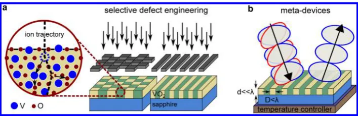
Figure 1. Optical meta-devices based on defect engineering of phase-transition materials. (a) The thermally driven insulator-to-metal phase transition of vanadium dioxide (VO2) can be modified by deliberately introducing structural defects into the lattice (defect engineering). Spatially selective defect engineering is achieved by ion beam irradiation through a mask. The enlarged area shows the primary displacement of both vanadium and oxygen lattice atoms by an incoming energetic ion and the subsequent damage cascade. The complex refractive indices of the insulating and metallic states are similar for the intrinsic and irradiated VO2, but the phase transition of the irradiated regions occurs at a much lower temperature (see alsoSupporting InformationS5). (b) The irradiated features can be made much smaller than the wavelength of light, so the resultingfilm becomes a metasurface with effective optical properties. One example is a tunable polarizer comprising stripes of irradiated and intrinsic VO2, creating a metasurface with a variable degree of optical anisotropy.
Figure 2. Defect engineering via ion beam irradiation. (a) Temper-ature-dependent transmittance (λ= 2.5μm) of a 100 nm VO2film on
c-plane sapphire irradiated with 75 keV Ar+ ions for various ion
fluences. The arrows mark the heating and cooling branches of the hysteresis curves. (b) Experimentally determined shift of the phase transition temperature (ΔTC) versus the calculated ndpa, given irradiation with 75 keV Ar+ and 190 keV Cs+ ions. The energy, mass, andfluence of the ion irradiation determine thendpa. The data points for Ar+and Cs+fall on the same curve and, because argon is not incorporated into the VO2lattice, we conclude that the shift of the critical temperature is a result of lattice defects induced by ion irradiation and is not caused by impurity doping. The exponential curve is a commonfit to both sets of points using a direct impact damage formation model (Supporting InformationS3).
Nano Letters Letter
DOI: 10.1021/acs.nanolett.5b04122
Nano Lett.2016, 16, 1050−1055
[image:3.625.64.298.301.445.2]using ion irradiation with various ions can be used to broadly tune the critical temperature of the IMT.
The IMT in VO2is particularly useful for tunable optical and
optoelectronic devices because it occurs gradually over a range of temperatures and provides access to a wide range of complex refractive index values.15,35,36 At the onset of the IMT, nanoscale islands of the metallic phase start to nucleate surrounded by insulating VO2, which then grow and connect in a percolation process.15Because of this phase coexistence on a subwavelength scale, VO2 in its transition region has been described as a natural disordered optical metamaterial.36 A similar gradual refractive index change can be observed in GST.37However, it has been noted that the intrinsic transition temperature of VO2 limits the utility of this material for devices.12Now using area-selective defect engineering with ion
fluences significantly smaller than the amorphization threshold of VO2, we can obtain control over the shape, temperature, and
persistence of the phase coexistence regions by selectively irradiating appropriate regions of the VO2 film, locally
modifying the IMT (Figure 1). In the temperature range where irradiated VO2 regions are metallic while the intrinsic
regions are insulating, persistent phase coexistence of metallic and insulating domains with a fixed metallic fraction is artificially induced.
We fabricated a sample composed of defect-engineered and intrinsic VO2 regions in a square checkerboard arrangement (period = 0.5μm) by irradiating a 100 nm VO2film onc-plane
sapphire with 190 keV Cs+ through a poly(methyl
meth-acrylate) (PMMA) mask made using electron-beam lithography (Figures 1a and3a). The ionfluence was set toNI= 1×10¹³
cm−2, which corresponds to ndpa= 0.05 (i.e., 5% of all lattice
atoms are displaced), and decreasesTCof the irradiated region to∼50°C (Figure 2b). We probed the temperature-dependent
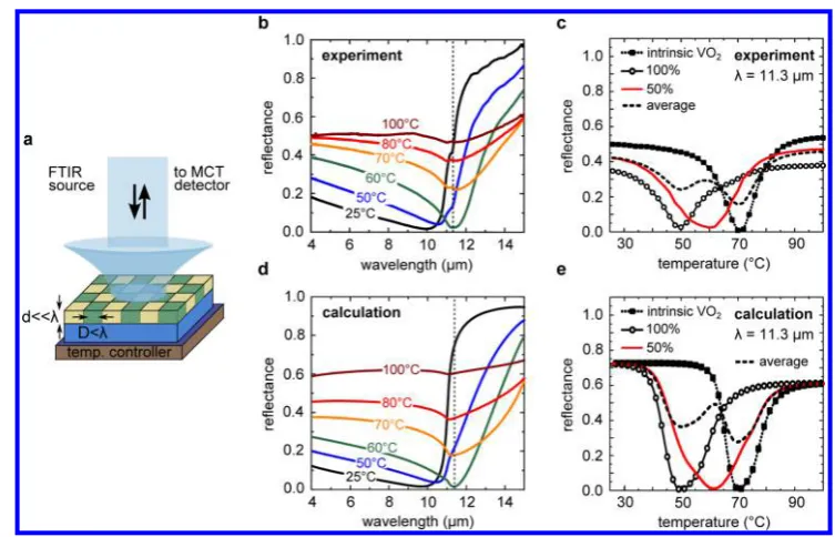
effective optical properties of this sample via mid-IR reflectance measurements using a Fourier transform infrared (FTIR) spectrometer and a mid-IR microscope (Figure 3). The mid-IR was chosen because the carrier concentration change due to the IMT leads to greater changes of the refractive index compared to the visible and near-infrared.
At low temperatures, both the irradiated and intrinsic VO2
regions are insulating and essentially transparent. The reflectance spectrum is dominated by the onset of a prominent Reststrahlen band of the sapphire substrate, leading to high reflectivity above∼11μm. As the temperature Tis increased, the mid-IR reflectance changes monotonically in the 4−10μm region and nonmonotonically in the 10−15 μm region, reaching a minimum-reflectance point at λ = 11.3 μm and
Tmin= 60°C. Such a reflectance minimum is also found in the
vicinity (∼3 °C below) of the phase transition at a metallic fraction of ∼33% in intrinsic and fully irradiated samples (Figure 3c, also seeSupporting InformationS5 and S6) and is a result of an “ultrathin-film interference condition” found in highly absorbingfilms on certain reflective substrates.35 Note that for sapphire, the wavelength at which this reflectance minimum appears is fixed to a relatively narrow range within the Reststrahlen band, where the complex refractive index is similar to that of metals at visible or UV frequencies and can be tuned slightly by the film thickness.35 Comparable complex refractive indices can also be found in a variety of other substrates in the visible and mid-IR, for instance, highly doped semiconductors and transparent conducting oxides.36
[image:4.625.121.498.62.304.2]In particular, the reflectance of the sample atλ= 11.3μm as a function of temperature (Figure 3c) shows that the subwavelength checkerboard structure possesses effective optical properties that cannot be trivially deduced by averaging the reflectance of the intrinsic and fully irradiated samples.
While the reflectance minimum of irradiated and intrinsic VO2
regions occurs independently at∼50 and∼70°C and has a full width at half-minimum (FWHM) of ∼15 and ∼12 °C, respectively, the subwavelength checkerboard appears to have a single effective reflectance minimum at ∼60 °C with a FWHM >25°C.
Because of the subwavelength nature of the checkerboard (“check”) pattern features, we can treat the patterned VO2film as an effective medium that has a well-defined temperature- and wavelength-dependent complex refractive index
̃ = ̃ ̃
neffcheck( )T nint( )T nirr( )T (1)
where ñint(T) and ñirr(T) are the temperature-dependent
refractive indices of intrinsic and irradiated VO2 regions, calculated from the refractive indices of insulating and metallic VO2, extracted from the measurements of Quazilbash et al.15 using the Bruggeman equation (seeSupporting InformationS6 and S7). Taking into account the effective optical constants, we used Fresnel equations to calculate the reflectance of the samples (Figure 3d, e,Supporting Information S6), which are in agreement with the measurements. Differing absolute reflectance values are most likely due to both a different optical quality of our intrinsic VO2sample compared to that in
ref 15, and an increasing amount of lattice defects after ion irradiation.
Our results show that the temperature range of phase coexistence can be greatly increased by patterned ion irradiation, because the metallic fraction will remain roughly constant in the temperature range between the transition temperatures of the irradiated and intrinsic VO2regions (e.g., between 50 and 70°C inFigure 3c). Furthermore, the metallic fraction can be adjusted by changingD. The optical properties can then be tuned in and out of an artificially designed effective medium state over a desired range of temperatures. We note that a vertical (rather than lateral) distribution of phase transition temperatures has been achieved in thin VO2 films synthesized from colloidal VOx nanocrystal solutions with
various tungsten doping densities.38
Further functionality can be achieved by realizing VO2-based
anisotropic metasurfaces with tunable dichroism. Anisotropic phase coexistence in thin VO2films has been observed on TiO2
substrates and occurs naturally due to strain39 but requires particular substrates and provides little control over the degree
of anisotropy. Similar phase coexistence was also achieved by selective laser heating of embedded VO2nanoparticles, though this structure is not temperature tunable.40
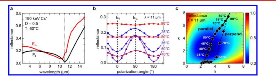
[image:5.625.88.554.58.186.2]We fabricated a periodic structure consisting of parallel ridges with a width of 0.5μm and a period of 1μm by irradiating a suitably masked sample with 190 keV Cs+ions at afluence of NI= 2×1013cm−2, corresponding tondpa= 0.09 (compare also Figure 1a). At a temperature where only the irradiated VO2is metallic, the reflectance from the patterned region is polar-ization-dependent over most of theλ= 2−15μm wavelength region, indicating a large degree of dichroism (Figure 4a, b). Especially at the wavelength at which minimal reflection occurs (λ= 11μm inFigure 4a), light polarized parallel to the ridges (E∥) is preferentially absorbed.
Figure 4b shows the measured polarization-dependent reflectance at λ = 11 μm as a function of increasing temperature. The reflectance is small from 40 to 70 °C for light polarized parallel to the ridges (E∥), and a value ofR∥ ∼
0.01 is reached atT ∼ 50 °C. At the same temperature, the reflectance for the orthogonal polarization is R⊥= 0.17. As a consequence, unpolarized light reflected from the patterned VO2 film becomes highly polarized with a degree of linear polarization (DOLP) of ∼90%, defined as intensity of light reflected with the preferential polarization minus the intensity of light reflected perpendicular to it divided by the sum of both.41The polarization dependence vanishes above 75°C, as both regions become metallic. Therefore, our device can be tuned in and out of the highly polarizing state by tuning the temperature.
To better understand the temperature- and polarization-dependent reflectance, we calculated the reflectance of a 100 nm thick anisotropically patterned VO2 film on sapphire for normally incident light that is polarized parallel (∥) or perpendicular to the ridges (⊥), respectively. When the wavelength is large enough, the refractive indices for a periodic structure consisting of ridges can be expressed as42
̃ = − ̃ + ̃
ngrid( )T [(1 D n) int2( )T Dnirr2( )]T 1/2 (6)
̃ = ̃ ̃
̃ + − ̃
⊥
n T n T n T
Dn T D n T
( ) [ ( ) ( )]
[ ( ) (1 ) ( )]
grid int irr
int2 irr2 1/2 (7)
Dis the area coverage (duty cycle) of the irradiated VO2and
ñint(T) and ñirr(T) are the temperature-dependent refractive Figure 4.Switchable polarizer via tunable anisotropy. (a) Measured reflectance of the anisotropic metasurface shown inFigure 1b, comprised of stripes of irradiated and intrinsic VO2(film thickness = 100 nm,D= 50%, period = 1000 nm) on a sapphire substrate. The sample temperature was maintained at 60°C, between the transition temperatures of the intrinsic and irradiated VO2, for light polarized parallel (E∥) and perpendicular (E⊥)
to the ridges. Light polarized parallel to the ridges is preferentially absorbed atλ∼11μm. (b) Evolution of the polarization-dependent reflectance at
λ= 11μm for increasing temperatures between 25 and 90°C. (c) Calculated map of the reflectance atλ= 11μm as a function of the real and imaginary part of the complex refractive indexñ=n+ikof an arbitrary 100 nmfilm on sapphire. The lamellar grid pattern is equivalent to a uniaxial crystal with form birefringence and dichroism. The solid (dashed) line marks the calculated temperature-dependent complex refractive index of a patterned VO2film for light that is polarized parallel (perpendicular) to the ridges.
Nano Letters Letter
DOI: 10.1021/acs.nanolett.5b04122
Nano Lett.2016, 16, 1050−1055
complex refractive index change in the mid-infrared is much greater than 1, whereas typical values achievable using, for example, the Kerr effect are no greater than ∼10−4.43 The predicted DOLP is 98% and can be improved to almost 100% by choosing an appropriatefilm thickness.
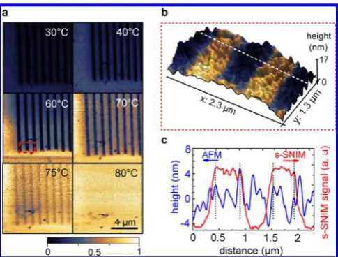
Although far-field measurements can probe the effective optical properties, the subwavelength patterns of irradiated VO2 cannot be resolved due to the diffraction limit. To explore the limits of our approach such as the sharpness of the boundary between irradiated and intrinsic areas, we performed near-field imaging (Figure 5). Mid-infrared near-field images at different
temperatures clearly show that the effective optical properties originate from the artificial phase coexistence and are not simply caused by a homogeneous distribution of diffused irradiation defects or long-range stress. Near-field images were obtained at temperatures from 30 to 80°C using a scattering scanning near-field infrared microscope (s-SNIM) at a wavelength of 10.9 μm and with a spatial resolution of ∼10 nm (Figure 5a). The s-SNIM signal is related to the local value
By comparing the near-field images with simultaneously acquired topography information, we observe that the spatial boundary between metallic (irradiated) and insulating (in-trinsic) VO2is not sharp but follows the domain boundaries. A
combined atomic force microscopy (AFM) and s-SNIM image of afilm at 60°C is shown in Figure 5b and a representative line scan through the ridges in Figure 5c. Because strain relaxation in thinfilms tends to terminate at grain boundaries, the best spatial resolution that can be achieved with our approach is reached when the domain size is on the order of the lateral straggle of ions in the film plane (∼15 nm, see
Supporting InformationS2).
Correlated phase-transition materials featuring insulator-to-metal transitions such as vanadium dioxide have a promising future as tunable components in optics and optoelectronics. The introduction of defect engineering as a robust method to engineer the phase transition on a subwavelength scale greatly expands the utility of these materials, enabling new types of optical meta-devices. We envision defect engineering as a way to bring the critical transition temperature of other phase-transition materials, such as rare earth nickelates, closer to room temperature, creating an ecosystem of defect-engineered tunable optical (meta)materials for applications such as optical switching, adaptive optics, and tunable thermal emission.
■
ASSOCIATED CONTENT*
S Supporting InformationThe Supporting Information is available free of charge on the
ACS Publications website at DOI: 10.1021/acs.nano-lett.5b04122.
Detailed description of the experimental methods. (PDF)
Additional information about the initial sample quality, effect of ion irradiation, optical calculations, and thermal stability of the samples. (PDF)
■
AUTHOR INFORMATIONCorresponding Authors
*E-mail: [email protected].
*E-mail: [email protected].
Author Contributions
J.R. and S.Z. contributed equally.
Notes
The authors declare no competingfinancial interest.
■
ACKNOWLEDGMENTSWe thank A. Kildishev for helpful comments. This work has been partiallyfinanced by the Initiative and Networking Fund of German Helmholtz Association, Helmholtz Virtual Institute VH-VI-422 MEMRIOX, DAAD program 57051746, ARO through Grant W911NF-14-1-0669, AFOSR through Grant FA9550-12-0189, and by Draper Laboratory:
[image:6.625.59.302.306.490.2]0000000731. S.Z. acknowledges support from the Singapore A*STAR National Science Graduate Scholarship. D.N.B. is the Moore Foundation Investigator in quantum materials, Grant GBMF4533. The fabrication and some of the measurements were performed at the Center for Nanoscale Systems (CNS) at Harvard University, a member of the National Nanotechnology Infrastructure Network (NNIN). Work at UCSD is supported through Grant ARO w911NF-13-1-0210.
■
REFERENCES(1) Smith, D. R.; Pendry, J. B.; Wiltshire, M. C. K.Science2004,305, 788−792 and references therein..
(2) Chen, H.-T.; Padilla, W. J.; Zide, J. M. O.; Gossard, A. C.; Taylor, A. J.; Averitt, R. D.Nature2006,444, 597−600.
(3) Zheludev, N. I.; Kiversushar, Y. S.Nat. Mater.2012,11, 917−924 and references therein..
(4) Ou, J. Y.; Plum, E.; Zhang, J.; Zheludev, N. I.Nat. Nanotechnol.
2013,8, 252−255.
(5) Yu, N.; Capasso, F.Nat. Mater.2014,13, 139−150.
(6) Zhao, Q.; Kang, L.; Du, B.; Li, B.; Zhou, K.; Tang, H.; Liang, X.; Zhang, B.Appl. Phys. Lett.2007,90, 011112.
(7) Werner, D. H.; Kwon, D.-H.; Khoo, I.-C.; Kildishev, A. V.; Shalaev, V. M.Opt. Express2007,15, 3342−3347.
(8) Yao, Y.; Shankar, R.; Kats, M. A.; Song, Y.; Kong, J.; Loncar, M.; Capasso, F.Nano Lett.2014,14, 6526−6532.
(9) Imada, M.; Fukimori, A.; Tokura, Y.Rev. Mod. Phys.1998,70, 1039−1263.
(10) Driscoll, T.; Kim, H.-T.; Chae, B.-G.; Kim, B.-J.; Lee, Y.-W.; Jokerst, N. M.; Palit, S.; Smith, D. R.; Ventra, M. D.; Basov, D. N.
Science2009,325, 1518−1521.
(11) Liu, M.; Hwang, H. Y.; Tao, H.; Strikwerda, A. C.; Fan, K.; Keiser, G. R.; Sternbach, A. J.; West, K. G.; Kittiwatanakul, S.; Lu, J.; Wolf, S. A.; Omenetto, F. G.; Zhang, X.; Nelson, K. A.; Averitt, R. D.
Nature2012,487, 345−348.
(12) Hosseini, P.; Wright, D.; Bhaskaran, H.Nature2014,511, 206− 211.
(13) Tittl, A.; Michel, A.-K. U.; Schäferling, M.; Yin, X.; Gholipour, B.; Cui, L.; Wuttig, M.; Taubner, T.; Neubrech, F.; Giessen, H.Adv. Mater.2015,27, 4597−4603.
(14) Yin, X.; Schäferling, M.; Michel, A.-K. U.; Tittl, A.; Wuttig, M.; Taubner, T.; Giessen, H.Nano Lett.2015,15, 4255−4260.
(15) Qazilbash, M. M.; Brehm, M.; Chae, B.-G.; Ho, P.-C.; Andreev, G. O.; Kim, B.-J.; Yun, S. J.; Balatsky, A. V.; Maple, M. B.; Keilmann, F.; Kim, H.-T.; Basov, D. N.Science2007,318, 1750−1753.
(16) Yang, Z.; Ko, C.; Ramanathan, S.Annu. Rev. Mater. Res.2011,
41, 337−367.
(17) Ladd, L. A.; Paul, W.Solid State Commun.1969,7, 425−428. (18) Jaramillo, R.; Ha, S. D.; Silevitch, D. M.; Ramanathan, S.Nat. Phys.2014,10, 304−307.
(19) Sheik-Bahae, M.; Hagan, D. J.; Van Stryland, E. W.Phys. Rev. Lett.1990,65, 96−99.
(20) Humar, M.; Ravnik, M.; Pajk, S.; Musevič ̌, I. Nat. Photonics
2009,3, 595−600.
(21) Kats, M. A.; Blanchard, R.; Genevet, P.; Yang, Z.; Qazilbash, M. M.; Basov, D. N.; Ramanathan, S.; Capasso, F. Opt. Lett.2013,38, 368−370.
(22) Townsend, P. D.; Chandler, P. J.; Zhang, L.Optical Effects of Ion Implantation; Cambridge University Press: New York, 1994.
(23) Shibuya, K.; Kawasaki, M.; Tokura, Y.Appl. Phys. Lett.2010,96, 022102.
(24) Kübler, C.; Ehrke, H.; Huber, R.; Lopez, R.; Halabica, A.; Haglund, R. F.; Leitenstorfer, A.Phys. Rev. Lett.2007,99, 116401.
(25) Jeong, J.; Aetukuri, N.; Graf, T.; Schladt, T. D.; Samant, M. G.; Parkin, S. S. P.Science2013,339, 1402−1405.
(26) Appavoo, K.; Lei, D. Y.; Sonnefraud, Y.; Wang, B.; Pantelides, S. T.; Maier, S. A.; Haglund, R. F., Jr.Nano Lett.2012,12, 780−786.
(27) Cao, J.; Ertekin, E.; Srinivasan, V.; Fan, W.; Huang, S.; Zhang, H.; Yim, J. W. L.; Khanal, D. R.; Ogeltree, D. F.; Grossman, J. C.; Wu, J.Nat. Nanotechnol.2009,4, 732−737.
(28) Park, J. H.; Coy, J. M.; Kasirga, T. S.; Huang, C.; Fei, Z.; Hunter, S.; Cobden, D. H.Nature2013,500, 431−434.
(29) Aetukuri, N. B.; Gray, A. X.; Drouard, M.; Cossale, M.; Gao, L.; Reid, A. H.; Kukreja, R.; Ohldag, H.; Jenkins, C. A.; Arenholz, E.; Roche, K. P.; Dürr, H. A.; Samant, M. G.; Parkin, S. S. P. Nat. Phys.
2013,9, 661.
(30) Brokate, M.; Sprekels, J. Hysteresis and Phase Transitions; Springer: New York, 1996.
(31) Zhao, L.; Miao, L.; Liu, C.; Li, C.; Asaka, T.; Kang, Y.; Iwamato, Y.; Tanemura, S.; Gu, H.; Su, H.Sci. Rep.2014,4, 7000.
(32) Wesch, W.; Wendler, E.; Schnohr, C. S.Nucl. Instrum. Methods Phys. Res., Sect. B2012,277, 58−69.
(33) Hofsäss, H.; Ehrhardt, P.; Gehrke, H.-G.; Brötzmann, M.; Vetter, U.; Zhang, K.; Krauser, J.; Trautmann, C.; Ko, C.; Ramanathan, S.AIP Adv.2011,1, 032168.
(34) Ufert, K. D.; Terukov, E. I.Phys. Stat. Sol. A1977,40, K157. (35) Kats, M. A.; Sharma, D.; Lin, J.; Genevet, P.; Blanchard, R.; Yang, Z.; Qazilbash, M. M.; Basov, D. N.; Ramanathan, S.; Capasso, F.
Appl. Phys. Lett.2012,101, 221101.
(36) Kats, M. A.; Blanchard, R.; Zhang, S.; Genevet, P.; Ko, C.; Ramanathan, S.; Capasso, F.Phys. Rev. X2013,3, 041004.
(37) Chen, Y. G.; Kao, T. S.; Ng, B.; Li, X.; Luo, X. G.; Luk’yanchuk, B.; Maier, S. A.; Hong, M. H.Opt. Express2013,21, 13691−13698.
(38) Paik, T.; Hong, S.-H.; Gaulding, E. A.; Caglayan, H.; Gordon, T. R.; Engheta, N.; Kagan, C. R.; Murray, C. B.ACS Nano2014,8, 797− 806.
(39) Liu, M.; Sternbach, A. J.; Wagner, M.; Slusar, T. V.; Kong, T.; Bud’ko, S. L.; Kittiwatanakul, S.; Qazilbash, M. M.; McLeod, A.; Fei, Z.; Abreu, E.; Zhang, J.; Goldflam, M.; Dai, S.; Ni, G.-X.; Lu, J.; Bechtel, H. A.; Martin, M. C.; Raschke, M. B.; Averitt, R. D.; Wolf, S. A.; Kim, H.-T.; Canfield, P. C.; Basov, D. N.Phys. Rev. B: Condens. Matter Mater. Phys.2015,91, 245155.
(40) Jostmeier, T.; Zimmer, J.; Karl, H.; Krenner, H. J.; Betz, M.
Appl. Phys. Lett.2014,105, 071107.
(41) Können, G. P.Polarized Light in Nature; Cambridge University Press: New York, 1985.
(42) Lalanne, P., Hutley, M. Artificial Media Optical Properties -Subwavelength Scale; Encyclopedia of Optical Engineering; Dekker: New York, 2007.
(43) Soref, R. A.; Bennet, B. R.IEEE J. Quantum Electron.1987,23, 123−129.
Nano Letters Letter
DOI: 10.1021/acs.nanolett.5b04122
Nano Lett.2016, 16, 1050−1055